HAL Id: hal-02159787
https://hal.archives-ouvertes.fr/hal-02159787
Submitted on 20 Jul 2019HAL is a multi-disciplinary open access archive for the deposit and dissemination of sci-entific research documents, whether they are pub-lished or not. The documents may come from teaching and research institutions in France or abroad, or from public or private research centers.
L’archive ouverte pluridisciplinaire HAL, est destinée au dépôt et à la diffusion de documents scientifiques de niveau recherche, publiés ou non, émanant des établissements d’enseignement et de recherche français ou étrangers, des laboratoires publics ou privés.
plasma-enhanced chemical vapor deposition using
atmospheric pressure plasma jet for microfluidic
applications
Samantha Bourg, Sophie Griveau, Fanny d’Orlyé, Michael Tatoulian, Fethi
Bedioui, Cédric Guyon, Anne Varenne
To cite this version:
Samantha Bourg, Sophie Griveau, Fanny d’Orlyé, Michael Tatoulian, Fethi Bedioui, et al.. Surface functionalization of cyclic olefin copolymer by plasma-enhanced chemical vapor deposition using atmo-spheric pressure plasma jet for microfluidic applications. Plasma Processes and Polymers, Wiley-VCH Verlag, 2019, 16 (6), pp.1800195. �10.1002/ppap.201800195�. �hal-02159787�
² ((please add journal code and manuscript number, e.g., DOI: 10.1002/ppap.201100001)) 1
Article type: Full paper
2 3
Surface Functionalization of Cyclic Olefin Copolymer by Plasma-Enhanced
4
Chemical Vapor Deposition using Atmospheric Pressure Plasma Jet for
5
Microfluidic Applications
6 7 8
Samantha Bourg, Sophie Griveau, Fanny d’Orlyé, Michael Tatoulian, Fethi Bedioui, Cédric 9
Guyon*, Anne Varenne* 10
11
––––––––– 12
13
Samantha Bourg, Dr. Sophie Griveau, Dr. Fanny d’Orlyé, Dr. Féthi Bedioui, Prof. Anne 14
Varenne* 15
Chimie ParisTech PSL, CNRS FRE 2027, Institute of Chemistry for Life and Health 16
Sciences, 11 rue Pierre et Marie Curie, 75005 Paris, France 17
E-mail: anne.varenne@chimieparistech.psl.eu 18
19
Prof. Michael Tatoulian, Dr. Cédric Guyon* 20
2PM (Plasma processes, Microsystems group) IRCP, Chimie ParisTech PSL, CNRS 8247, 11 21
rue Pierre et Marie Curie, 75005 Paris, France 22 E-mail: cedric.guyon@chimieparistech.psl.eu 23 24 25 ––––––––– 26
Lab-On-A-Chips promise solutions for high throughput and specific analysis for environment 27
and health applications, with the challenge to develop materials allowing fast, easy and cheap 28
microfabrication and efficient surface treatment. Cyclic Olefin Copolymer (COC) is a 29
promising thermoplastic, easily microfabricated for both rapid prototyping and low-cost mass 30
production of microfluidic devices, but still needing efficient surface modification strategies. 31
This study reports for the first time the optimization of an easy COC silica coating process by 32
Plasma-Enhanced Chemical Vapor Deposition at Atmospheric Pressure (APPECVD) with 33
plasma jet and tetraethylorthosilicate (TEOS) as precursor, leading to a 158±7 nm thickness 34
and a 14 days stability of hydrophilic properties for a COC-embedded microchannel (100 35
µm), paving the way for a simplified and controlled COC surface modification. 36
` 37 38 39
40
1
Introduction
41 42
Lab-On-A-Chip (LOAC) technology promises solutions for high throughput and highly 43
specific analysis for environment and health applications. The choice of the material to 44
engineer them is crucial. Indeed, each material has its own physicochemical properties which 45
determine the microfabrication method. Moreover, it is sometimes necessary to modify the 46
physico-chemical properties of the microchannel surface for subsequent functionalization 47
and/or fluid flow control. Therefore, the challenge is to develop LOAC materials allowing 48
fast, easy and cheap microfabrication methods and efficient surface treatment. Since nearly 49
20 years poly(dimethyl siloxane) (PDMS) has been a popular material for the fabrication of 50
microfluidic devices due to its easy microfabrication method, its elastic and transparency 51
properties and its biocompatibility.[1,2] However, there is nowadays a move towards 52
thermoplastic materials for their reduced cost and easier microfabrication.[3–7] Among the 53
various thermoplastics, cyclic olefin copolymer (COC) has emerged as it offers a high 54
chemical resistance and exhibits an optical transparency close to that of glass (for 55
wavelengths over 300 nm).[8] COC microsystems are furthermore easily micro fabricated 56
allowing for both rapid prototyping and low-cost mass production.[9,10] 57
Despite all these advantages, COC’s main drawbacks as a material for microfluidics are its 58
surface chemical inertness and its hydrophobic properties. In the case of LOACs, the 59
integration of the different steps of an analytical chain (pre-concentration, separation and 60
detection) in microchannels mainly implies a chemical modification of the COC surface. 61
Some COC microchannel treatments provide hydrophilic properties to control electrokinetic 62
separations[11–15] or to integrate chemical reactive groups for ligands[12,13,16–19] or monolith[20– 63
22]
immobilization. Moreover, surface functionalization of COC micro channels minimizes the 64
adsorption of analytes in particular biological molecules.[11,14,18,23] Nowadays, three main 65
COC surface functionalization strategies are commonly used: UV/ozone oxidation,[24,25] 66
photografting[11,13,15,20,21,23,26–29] and plasma processes[16,19,30–36]. 67
The UV/ozone oxidation procedure relies on the exposition of the COC surface under a 68
mercury lamp and in an air-filled chamber at atmospheric pressure resulting in the generation 69
of ozone. This treatment permits to confer hydrophilic properties to COC surfaces.[24,25] 70
Photografting is performed by a photoinitiator under a UV light, which excitation promotes 71
abstraction of hydrogen atoms from the COC surface, leading to the formation of radicals 72
which then initiate a surface grafting polymerization process.[37] Generally, photografting is 73
performed through a single step, that can lead to a significant amount of ungrafted 74
polymer.[23] 75
Plasma is widely used for COC surfaces treatment[16,19,30–35,38], so as to shift the COC surface 76
to a hydrophilic one, due to its oxidation, molecule chain scissions, substitution and 77
recombination[31,38]. Several gases or gas mixtures have been extensively used for plasma 78
generation such as oxygen, argon or nitrogen.[30–32,38] The main advantages of this surface 79
treatment are that it is an environmentally benign process and leads to a homogeneous 80
surface.[30–32,38] 81
One renowned plasma process to deposit chemical layer on surfaces is Plasma-Enhanced 82
Chemical Vapor Deposition (PECVD).[39] This low-pressure plasma process consists in the 83
fragmentation of a precursor inside gas plasma. Organosilicon-oxygen mixtures are widely 84
used to generate thin silica film deposition, notably for microfluidic applications.[35–36] The 85
thin silica layer confers hydrophilic properties allowing the generation of a controlled 86
electroosmotic flow for electrokinetic separations inside COC microchannels.[40] Moreover, 87
the presence of reactive chemical functions, such as silanol groups (SiOH), due to plasma 88
polymerization of organosilicon precursors,[35–36] could allow the grafting of several chemical 89
entities[41–42]. Da Silva et al. have shown the possibility to deposit by PECVD at low pressure 90
thin layers of silica (700 nm thickness) on COC surface.[36] This layer was characterized by 91
water contact angle (WCA), X-ray photoelectron spectroscopy (XPS), Fourier-transform 92
infrared spectroscopy (FTIR) and ellipsometry measurements, showing the presence of a 93
silica film on the COC substrate. Ladner et al. demonstrated the activation of COC surface by 94
a plasma at low pressure composed of 1-bromopropane as the brominated precursor and of 95
argon gas, to create brominated functionalities that could permit to immobilize ligands 96
through subsequent chemical modifications via a click chemistry reaction. [19] 97
The main drawback of many plasma treatments is the use of low pressures leading to 98
expensive and cumbersome plasma equipments hardly adapted for industrial continuous 99
operations.[43] Moreover, generation of a vacuum could take several hours, depending on the 100
vacuum required, and increase the overall process time. To overcome this, plasma surface 101
treatments were further developed at atmospheric pressure. A study has demonstrated the 102
possibility to deposit a thin silica film in few minutes inside COC microchannels at 103
atmospheric pressure with organosilicon precursor.[35] The silica layer was deposited with a 104
helium-oxygen plasma generated between two electrodes integrated outside the chip and an 105
organosilicon precursor circulating inside the COC channel. 106
This study reports, for the first time, the deposition of a silica coating inside COC 107
microchannel with a plasma jet at atmospheric pressure. Plasma jet is advantageous over 108
plasma treatments at atmospheric pressure proposed by Theelen et al.[35] Indeed, it does 109
neither need the integration and the alignment of electrodes outside the chip, nor a gas flow 110
through the microchannel, which greatly simplifies the microfabrication steps and avoids the 111
use of several external equipments. Moreover, the plasma jet permits to treat several 112
microchannels simultaneously in a few seconds. The experimental conditions for this COC 113
surface modification with tetraethylorthosilicate (TEOS) were optimized so as to obtain a 114
homogeneous density of silanol groups on its surface, for further functionalization and for the 115
generation of an electroosmotic flow inside COC microchannels. Experimental conditions 116
were optimized in terms of distance between the nozzle and the substrate, TEOS and carrier 117
air flow rates, and number of treatment cycles. The treatment of COC channels by the 118
Atmospheric Pressure plasma jet proved to be fast and easily transposable for industrial 119
applications. This process does not require complicated microfabrication steps, is 120
environmentally friendly and will allow to design new LOACs involving COC materials. 121
122
2
Materials and Chemicals
123 124
COC plates (Topas® grade 8007, Tg = 75°C, 1 mm thickness) were purchased from 125
Microfluidic ChipShop. Brass mold (8 cm * 8 cm * 5 mm) was purchased from GREM 126
(France). Silica wafers (4 inches, 500 µm of thickness) were purchased from Prolog Semicor 127
(Ukraine). Tetraethylorthosilicate (TEOS, 98%), was purchased from Sigma-Aldrich. 128
2-propanol (99.9%) was purchased from GPR Rectapur. Ultra-pure water (resistivity ≥ 18.2 129
MΩ, Purelab Flex, Elga Veolia, France) was used. 130
131 132 133
3
General Procedure for the Silica-Like Deposition Using AcXys
®134
plasma jet on COC Surface
135 136
In this study, the silica thin film has been deposited with an atmospheric pressure plasma 137
system produced by AcXys® Technologies (Saint Martin le Vinoux, France). This system is 138
composed of three command modules and a moving nozzle. The frequency is set with ULS 139
command module where the power and the gas throughout are displayed. Thus, the APPJ 140
(Atmospheric Pressure Plasma Jet) nozzle is mounted on a motorized xyz table (controlled 141
using the Quickset module) so that it can sweep the surface of the sample at constant speed 142
(fixed at 150 mm/s) in order to deliver a homogeneous treatment. The plasma jet is generated 143
by introducing air (35 L/min) into the plasma torch. The ULC module is used to inject the 144
liquid organosilicon precursor (TEOS) contained in a pressurized tank into the treatment 145
nozzle at a flow rate between 10 µL/min and 500 µL/min. The carrier gas (at a flow rate 146
between 5 L/min and 25 L/min) vaporizes the liquid precursor which is then injected in post-147
discharge via pipes placed on each side of the nozzle. It should be noticed that the liquid 148
precursor is controlled by a liquid flow meter before being nebulized by the venturi effect. 149
The precursor thus nebulized is transported by the carrier gas to the deposition nozzle. The 150
system operates at room temperature. 151
152
Figure 1. Picture of the torch plasma AcXys®. 153
154
4
Microfabrication of COC Channels
155 156
The design of channels was performed with the 3D CAO software Inventor® and then 157
transposed on a brass mold with micro-molding technic (Minitech®). Afterwards, hot 158
embossing was applied to COC (75 mm * 25 mm * 1 mm) plates, inside a 3 tons hydraulic 159
press (Scannex®) at 150°C, under a 15 bars pressure for 30 min. The system was then cooled 160
at room temperature before shutting off the pressure. The dimensions of simple COC 161
rectangular microchannels used during the study are of 6 cm length, 100 µm width and 30 µm 162
height. 163
164
5
Characterizations of the Silica-Like Deposition on COC Surface
165
COC raw plates and COC treated plates are characterized by the following methods. Infrared 166
spectra were acquired using a Fourier Transform Infrared Spectrometer (Cary 660 167
Spectrometer, Agilent) with an Attenuated Total Reflectance module (GladiATR, Pike). The 168
ATR-FTIR spectra were collect from 4 000 to 500 cm-1, at a resolution of 4 cm-1. 100 scans 169
were made for each measurement. The background (air) was taken before each measurement. 170
Static ultrapure water (resistivity ≥ 18.2 MΩ) contact angle (WCA) measurements were done 171
thanks to a DSA25-Drop Shape Analyser from Krüss. A 2 µL droplet was released from a 172
syringe and placed slowly on the surface which contact angle was measured after 30 s. 173
Similar experiment were conducted on the modified material after 14 days of storage in a petri 174
dish at room temperature and at atmospheric pressure to simulate the COC microchips storage 175
conditions. Images of droplet formation captured using a high-resolution camera were 176
analyzed with the Advance Image Analysis Software. The reported contact angle values are 177
an average at least three measurements at various locations on COC plates. 178
Optical microscopy (Axio Observer A1, Zeiss) was performed with a CCD digital camera 179
(Pike F145B, Allied Vision Technologies Stadtroda, Germany) and an image acquisition 180
software (Hiris, RD Vision, France). Images were reprocessed via Image J software. 181
Spectroscopic ellipsometry (UVISEL, Horiba Jobin Yvon) was performed at an incidence 182
angle of 60°, with a 75 W Xe lamp over a spectral range of 245±2100 nm (i.e., 0.6±5 eV). 183
Ellipsometry is based on variation of light polarization, which is reflected by the sample.[44] 184
As COC substrates do not reflect light,[8] a silica wafer was chosen as model substrate to 185
determine the thickness of silica deposits[19]. The reported thickness values are an average of 186
at least three measurements at various locations on modified of plate surfaces. 187
188
6
Results and Discussion
189 190
As a preliminary treatment, COC plates were sonicated in isopropanol and then water (during 191
3 min). When treated with the plasma jet, COC plates were attached with carbon tape on a 192
holder. So as to remove eventual low molecular weight fragments at the topmost COC surface 193
layer,[36] they were pre-treated by Air Plasma at Atmospheric Pressure (APAP) at 80 kHz (987 194
W, 35 L/min air) with a nozzle speed of 150 mm/s. Indeed, oxygen radicals and excited 195
molecules produce volatile organic and inorganics compounds such as CO, CO2, H2O
196
molecules, eliminating low molecular weight oxidized fragments. In a second step, a silica 197
film was then deposited on COC surfaces by APPECVD process, under an air plasma to 198
decompose TEOS 80 kHz (1030 W, 35 L/min air) with a nozzle speed of 150 mm/s. The 199
APPECVD process could be applied several times, “a treatment cycle” being defined as one 200
APPECVD process. 201
The influence of several experimental parameters on the silica coating of COC substrates (2 202
cm2) was studied. These parameters are the distance between the nozzle and the substrate 203
surface (from 16.5 to 31.5 mm), the TEOS flow rate (from 100 µL/min to 200 µL/min), the 204
carrier air flow rate (from 5 to 20 L/min), and the number of treatment cycles (from 1 to 5). 205
The COC plates before treatment, after the APAP step, and after APAP + APPECVD were 206
characterized by ATR-FTIR, WCA and optical microscopy. The thickness of silica layers was 207
measured by ellipsometry. 208
209 210
6.1 Characterizations of Untreated and Plasma Treated COC Plates
212
Figure 2 shows ATR-FTIR (Figure 2.a) and optical microscopy characterizations (Figure 213
2.b) of COC surfaces, either before any treatment, after APAP treatment and after APAP+
214
one APPECVD cycle. The water contact angle measurements were done for each step of the 215
silica deposit process. The thickness of the silica layer after APPECVD treatment was also 216
measured. 217
218
Figure 2. COC substrate characterizations before any treatment (bottom graph and image),
219
after APAP treatment (middle graph and image) and after APAP + APPECVD treatments
220
(upper graph and image) by (a) ATR-FTIR, and (b) optical microscopy. Experimental
221
conditions for APAP: 16.5 mm between torch and surface and 150 mm/s nozzle speed (~300
222
ms treatment time). Experimental conditions for APPECVD: 16.5 mm between torch and
223
surface, 200 µL/min TEOS, 5 L/min carrier air and 150 mm/s nozzle speed (~300 ms
224
treatment time).
225 226
Untreated COC surfaces present an ATR-FTIR spectrum (Figure 2.a) with absorption bands 227
located at 2947 and 2868 cm-1 which are assigned to carbon/hydrogen stretching vibration 228
modes of -CH2 and -CH3 groups from the polymer backbone. The band around 1456 cm-1
229
corresponds to the wagging mode of -CH3 groups.[36] The WCA measurements of untreated
230
COC plate (95±1°) confirmed the hydrophobic properties of the polymer.[8] Optical 231
microcopy characterization showed that the COC surface was transparent and homogeneous 232
(Figure 2.b).[8] 233
234
The ATR-FTIR spectrum of APAP-treated COC surface did not present any difference with 235
that of the untreated COC surface (Figure 2.a). After APAP treatment, the WCA values 236
dropped from 95±1° to 48±7°. This can be explained by the insertion of polar functional 237
groups onto the surface of the raw hydrophobic COC substrate after APAP 238
treatment,[30,33,34,38,45] leading to a more hydrophilic surface. ATR-FTIR spectroscopy is not 239
sensitive enough to detect the presence of polar groups deposited by APAP treatment. Roy et 240
al. have suggested a possible reaction mechanism on COC surface during plasma 241
treatment[,38], the electrons, ions and free radicals generated during high energy plasma 242
irradiation promoting breakage of the C-H and C-C bonds. This would lead to shorter polymer 243
carbon chain, the formation of other molecules through recombination reaction and also 244
crosslinking.[38] As nitrogen and oxygen atoms are present, chemical interactions between the 245
radicals from air and thermoplastics occur, which promote the insertion of polar groups like 246
hydroxyl, ketone or carboxylic acid for example.[32] Optical microcopy characterization 247
showed that APAP-treated COC surface did not present any difference compared to untreated 248
COC (Figure 2.b). APAP treatment preserved the optical transparency of the substrate. 249
250
After APPECVD treatment, three new ATR-FTIR bands appeared in addition to the 251
characteristic bands of COC backbone. During APPECVD treatment, a silica layer was 252
deposited due to the reaction between oxygen reactive atoms and the precursor, generating 253
emission of carbon dioxide and water.[36] The two bands at 1225 cm-1 and 1078 cm-1 254
correspond to the Si-O-Si asymmetrical and symmetrical stretching modes, respectively.[36,46] 255
The band located at 3342 cm-1 is assigned to hydroxyl group (stretching mode). This band is 256
related to the presence of Si-OH groups, as the interaction between the -SiO2 layer and the air
leads to the formation of –OH groups at the outer surface of the coating.[36] The initial bands 258
originating from the COC thermoplastic backbone (2947, 2868 and 1456 cm-1) were still 259
present due to the low thickness of the silica layer (39±5 nm) compared to the depth to the 260
analysis .[36] The WCA values dropped from 48±7° to 27±2° for APAP- and APAP + 261
APPECVD-treated COC surface, respectively, evidencing the deposition of a more 262
hydrophilic layer. Optical microscopy characterization shows that APPECVD treatment 263
induced micro-cracked surface layer (Figure 2.b). 264
In order to generate a homogeneous immobilization of ligands/monoliths or a repeatable 265
electroosmotic flow between various batches of COC LOACs, the surface layer should be as 266
homogeneous as possible. Micro-cracks may be due to the generation of an elevated 267
temperature during plasma treatment that could degrade the surface. By increasing the 268
distance between the nozzle and the substrate, temperature during the treatment should be 269
lowered. 270
271
6.2 Influence of the Distance Between the nozzle and the Surface on the Silica
272
Coating
273 274
To avoid the presence of cracks evidenced on APAP + APPECVD-treated COC surface, 275
probably caused by a too high treatment temperature process, the distance between the torch 276
and the substrate was increased, step by step (by 5 mm), from 16.5 mm and 31.5 mm. The 277
increase in this distance should allow reducing the temperature during the treatment. The 278
study was performed in the same experimental conditions as previously described except for 279
the distance between the torch and the substrate. For each distance, the thickness of the silica 280
layer was measured by ellipsometry and the presence of cracks was checked by optical 281
microscopy (Table 1). 282
Table 1. Influence of the distance between the torch and the COC surface on the silica layer
284
thickness determined by ellipsometry. For experimental conditions for silica deposition, see
285
Figure 2.
286
287
When torch/substrate distance was increased, the silica layer thickness decreased 288
concomitantly. This can be explained by the fact that, air/TEOS plasma spot reaches the COC 289
surface with a large diameter, leading to less TEOS reactive species density onto the COC 290
surface. The cracks were no more visible when applying a distance of 31.5 mm. For all the 291
tested distances, the wettability did not change, with a constant value of ˜30°. 292
293 294 295 296
6.3 Influence of the TEOS flow rate and number of treatment cycles
297 298
The influence of the TEOS flow rate (100 and 200 L/min) and the number of treatment 299
cycles (1, 3 and 5) on the properties of the deposited silica layer were studied by ATR-FTIR, 300
WCA and ellipsometry (Figure 3). For this study, the carrier air flow rate was fixed at its high 301
value (20 L/min) to consider a high silica and silanol density, for a better sensitivity with 302
ATR-FTIR measurements. 303
Distance between the torch and the surface of the substrate
[mm]
Silica coating thickness [nm] Presence of cracks 16.5 39±5 Yes 21.5 43±11 Yes 26.5 38±8 Yes 31.5 20±3 No
304 305 306 307 308 309 310 311 312 313 314 315 316 317 318 319 320 321 322 323 324 325 326
Figure 3. COC substrate characterizations (ATR-FTIR, WCA and ellipsometry) after the
327
overall plasma treatment: (APAP followed by 1 (˜300 ms), 3 (˜900 ms) or 5 (˜1.5 s)
328
APPECVD treatment cycles. Experimental conditions for APAP pre-treatment: 31.5 mm
329
between torch and surface, 1 cycle treatment (300 ms). Experimental conditions for
330
APPECVD: 31.5 mm between torch and surface, (a) 100 or (b) 200 µL/min of TEOS and 20
331
L/min of carrier air flow rate.
For each TEOS flow rate, the peak intensities attributed to the silica thin film (3342, 1225 and 333
1078 cm-1) increased with the number of treatment cycles. On the other side, peak intensities 334
originating from the thermoplastic backbone (2947, 2868 and 1456 cm-1) decreased when 335
increasing the number of cycles (Figure 3). These results are consistent with an increase in 336
silica deposit with the number of cycles. These results furthermore indicate that wettability 337
increased with the number of treatment cycles. Concerning ellipsometry measurements, the 338
layer thickness was confirmed to increase with the number of treatment cycles. 339
Moreover, the TEOS flow rate played a key role on the silica layer characteristics. The 340
intensity of the band attributed to -OH groups from silanol (3342 cm-1) was twice higher at 341
200 µL/min (5 cycles) compared to 100 µL/min (5 cycles) of flow rate (Figure 3). The higher 342
the flow rate, the more hydrophilic the treated surface and the thicker the layer. This result is 343
in accordance with previous studies.[47] So a higher silica density was deposited with the 344
higher TEOS flow rate on COC surface. Optical microscopy characterizations were done to 345
verify the absence of visible cracks with all combinations of experimental conditions tested. 346
For all of them, no crack on the surface treated by APAP + APPECVD were noticed (data not 347
shown). 348
349 350
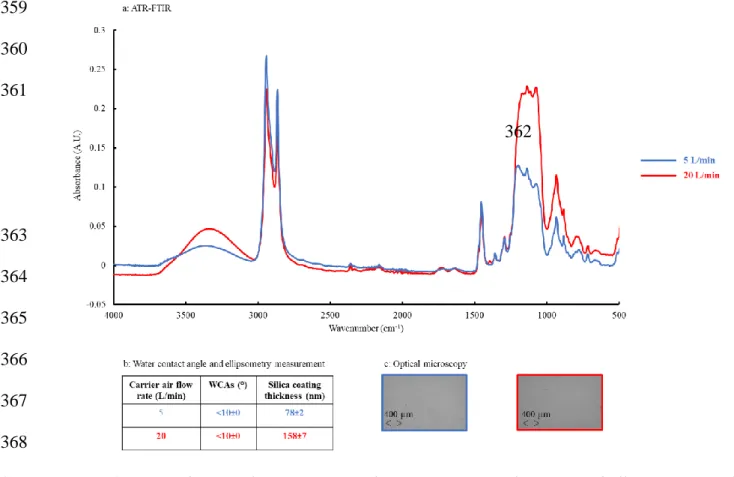
6.4 Influence of the Carrier Air Flow Rate
351 352
Another experimental parameter for the optimization of the silica layer is the carrier air flow 353
rate, which was varied from 5 to 20 L/min. For each flow rate, ATR-FTIR, WCA and 354
ellipsometry measurements were performed and the presence of cracks was checked by 355
optical microscopy (Figure 4). 356
357 358
359 360 361 362 363 364 365 366 367 368
Figure 4. COC substrate characterizations by (a) ATR-FTIR, (b) WCA and ellipsometry, and
369
(c) optical microscopy after APAP and 5 APPECVD treatment cycles. Experimental
370
conditions for APAP pre-treatment: 31.5 mm between torch and surface, 1 cycle (300 ms).
371
Experimental conditions for APPECVD: 31.5 mm between torch and surface, 200 µL/min of
372
TEOS, 5 treatment cycles (1.5 s) and 5 (blue) or 20 L/min (red) of carrier air flow rate.
373 374
ATR-FTIR spectra indicate that the absorbance of the bands attributed to the silica layer 375
(3342, 1225 and 1078 cm-1) increased with the carrier air flow rate, whereas the absorbance of 376
the bands originating from the thermoplastic backbone (2947, 2868 and 1456 cm-1) decreased 377
(Figure 4.a). The thickness of the silica layer increased from 78±2 nm to 158±7 nm, when the 378
carrier air flow increased from 5 L/min to 20 L/min (Figure 4.b). It therefore seems that the 379
increase in carrier air flow leads to higher silanol density on plasma treated COC 380
thermoplastic (Figure 4.a and 4.b). This can be explained by an increase in interaction 381
between SiO2 layer and the air, as reported in the literature.[38] With 5 L/min and 20 L/min
382
carrier air flow rates, the optical characterizations of the surface proved the absence of crack 383
on the silica deposit (Figure 4.c). Therefore, the objective to obtain a sufficient and 384
homogeneous surface silanol density for further functionalization[41-42 can be reached with the 385
following APPECVD conditions: a 31.5 mm distance between the torch and the surface, 200 386
µL/min TEOS flow rate, 20 L/min carrier air flow rate and 5 treatment cycles. This COC 387
surface modification should allow the generation of a controlled electroosmotic flow inside 388
COC microchannels [40].The silica layer was then of 158±7 nm thickness with a contact angle 389
of less than 10°. These performances are similar to the ones of other plasma processes on 390
COC surfaces for silica deposition in terms of layer thickness (between 250 nm[35] and 700 391
nm[36] for atmospheric pressure and low pressure plasma respectively) and wettability (~10°). 392
The plasma process described herein relies on simplified conditions in terms of equipements, 393
treatment rapidity and costs[41] and allows generating the deposition of a silica layer on COC 394
surface with a similar wettability and the same order of magnitude for the silica layer 395
thickness (between 100 and 900 nm) as the plasma process at low pressure 396
397
6.5 Stability of the Silica Layer
398 399
The stability of the silica layer deposited using the optimized experimental conditions 400
(APPECVD: 31.5 mm between torch and surface, 200 µL/min TEOS flow rate, 20 L/min 401
carrier air flow rate and 5 treatment cycles) was studied by WCA measurements. APAP + 402
APPECVD-treated COC plate was stored in a petri-dish at room temperature and at 403
atmospheric pressure for 14 days to simulate the COC microchips storage conditions. As a 404
matter of comparison, untreated COC surface and APAP-treated COC plates were stored and 405
studied under the same conditions (Figure 5). 406
407
Figure 5. Evolution of WCA measurements in function of storage time (0 to 14 days) for raw
408
(COC), pre-treated with APAP (COC + APAP) and fully treated (COC + APAP +
409
APPECVD) COC surface. Storage conditions: in petri-dish at atmospheric pressure and
410
room temperature. Experimental conditions for APAP: 31.5 mm between torch and surface
411
and 1 cycle (300 ms). Experimental conditions for APPECVD: 31.5 mm between torch and
412
surface, 200 µL/min TEOS flow rate, 20 L/min carrier air flow rate and 5 treatment cycles
413
(1.5 s).
414 415
As shown in Figure 5, silica layers deposited on COC surface are stable over 14 days, in 416
accordance with another study.[36] The COC plates with a APAP + APPECVD plasma 417
treatment can thus be stored during 2 weeks at atmospheric pressure and room temperature 418
before further processing. 419
420
6.6 Optical Characterization of Plasma Treated COC Microchannels
421 422
So as to evaluate the transposition of our process into COC microchannels, preliminary 423
experiments were conducted using optimized conditions for silica coating in single COC 424
microchannels of 6 cm length, 100 µm width and 30 µm height. Optical characterizations of 425
COC microchannels were performed before and after APAP + APPECVD treatment, as 426
illustrated in Figure 6. 427
428
429
Figure 6. Optical characterizations of COC microchannels (a) before and after (b) silica
430
coating by plasma treatment at atmospheric pressure. Experimental conditions for APAP and
431
APPECVD: see Figure 5. Fully treatment time (COC + APAP + APPECVD) microchannel is
432
˜2.4 s. The black line is 100 µm bar scale.
433 434
This figure shows that scratches inside COC microchannel due to the brass mold can be 435
observed (Fig 6 a). After APAP + APPECVD treatment, almost all scratches disappeared, 436
probably screened by the deposition of a thin silica layer into the microchannel (Figure 6.b). 437
The thin silica layer overlaid the defects inside COC microchannels. These results prove the 438
efficient transposition of the in situ plasma process, inside microdevices. 439 440 441 442 443
7
Conclusion
444 445This study reports for the first time a new plasma process for simplified, quick and efficient 446
silica layer deposition on COC surfaces. This new procedure employs Plasma-Enhanced 447
Chemical Vapor Deposition at Atmospheric Pressure (APPECVD) with a plasma jet, TEOS 448
as precursor and air gas. The optimization of different experimental conditions allowed to 449
generate a homogeneous silica coating on COC surface. The optimal experimental conditions 450
permitted to deposit a 158±7 nm hydrophilic silica layer that proved to be stable over 14 days 451
stored at room temperature and atmospheric pressure. 452
This fast and versatile plasma process compared to the ones generated at low pressure, 453
allowed to deposit thin silica layers of similar properties on COC substrate. This plasma jet 454
treatment also allowed in situ treatment of COC microchannels, that is to say fast and easy 455
microfabrication process of the microchips, is environmentally friendly and can be further 456
used for industrial application, among which the production of COC LOAC. 457
Acknowledgements: Ecole Doctorale 406 (PSL and Sorbonne Université) is acknowledged 458
for its financial support. This work has received the technical support of "Institut Pierre-Gilles 459
de Gennes" (laboratoire d’excellence, “Investissements d’avenir” program ANR-10-IDEX-460
0001-02 PSL and ANR-10-LABX-31.). 461
462
Received: ((will be filled in by the editorial staff)); Revised: ((will be filled in by the editorial 463
staff)); Published online: ((please add journal code and manuscript number, e.g., DOI: 464
10.1002/ppap.201100001)) 465
466
Keywords: APPECVD; COC; silica coated; TEOS; microfluidic. 467
468 469
[1] Y. Xia and G. M. Whitesides, Angew. Chem. Int. Ed. 1998, 37, 550. 470
[2] J. Zhou, A. V. Ellis and N. H. Voelcker, Electrophoresis 2010, 31, 2. 471
[3] T. B. Stachowiak, F. Svec and J. M. Fréchet, J. Chromatogr. A. 2004, 1044, 97. 472 [4] K. Faure, Electrophoresis 2010, 31, 2499. 473 [5] M. Pumera, Talanta 2005, 66, 1048. 474
[6] D. Wu, J. Qin and B. Lin, J. Chromatogr. A. 2008, 1184, 542. 475
[7] K. Ren, J. Zhou and H. Wu, Acc. Chem. Res. 2013, 46, 2396. 476
[8] P. S. Nunes, P. D. Ohlsson, O. Ordeig and J. P. Kutter, Microfluid. Nanofluidics 2010, 9, 477
145. 478
[9] R. Novak, N. Ranu and R. A. Mathies, Lab. Chip 2013, 13, 1468. 479
[10] U. M. Attia, S. Marson and J. R. Alcock, Microfluid. Nanofluidics 2009, 7, 1. 480
[11] C. Li, Y. Yang, H. G. Craighead and K. H. Lee, Electrophoresis 2005, 26, 1800. 481
[12] A. Muck and A. Svatos, Talanta, DOI:10.1016/j.talanta.2007.09.012. 482
[13] Q. Pu, O. Oyesanya, B. Thompson, S. Liu, and J. C. Alvarez, Langmuir 2007, 23, 483
1577. 484
[14] J. Zhang, C. Das and Z. H. Fan, Microfluid. Nanofluidics 2008, 5, 327. 485
[15] S. Roy, T. Das and C. Y. Yue, ACS Appl. Mater. Interfaces 2013, 5, 5683. 486
[16] C. Jönsson, M. Aronsson, G. Rundström, C. Pettersson, I. Mendel-Hartvig, J. Bakker, 487
E. Martinsson, B. Liedberg, B. MacCraith, O. Öhman and J. Melin. Lab. Chip 2008, 8, 488
1191. 489
[17] J. Raj, G. Herzog, M. Manning, C. Volcke, B. D. MacCraith, S. Ballantyne, M. 490
Thompson, D. W. M. Arrigan, Biosens. Bioelectron. 2009, 24, 2654. 491
[18] D. Sung, D. H. Shin and S. Jon, Biosens. Bioelectron. 2011, 26, 3967. 492
[19] Y. Ladner, F. d'Orlyé, C. Perréard, B. Da Silva, C. Guyon, M. Tatoulian, S. Griveau, 493
F. Bedioui and A. Varenne, Plasma Process. Polym. 2013, 10, 959. 494
[20] T. B. Stachowiak, D. A. Mair, T. G. Holden, L. J. Lee, F. Svec, J. M. J. Fréchet, 495
Electrophoresis 2003, 24, 3689.
[21] K. Faure, M. Albert, V. Dugas, G. Crétier, R. Ferrigno, P. Morin and J.-L. Rocca, 497
Electrophoresis 2008, 29, 4948.
498
[22] J. Liu, C.-F. Chen, C.-W. Tsao, C.-C. Chang, C.-C. Chu and D. L. DeVoe, Anal. 499
Chem. 2009, 81, 2545.
500
[23] T. B. Stachowiak, D. A. Mair, T. G. Holden, L. J. Lee, F. Svec and J. M. Fréchet, J. 501
Sep. Sci. 2007, 30, 1088.
502
[24] C. W. Tsao, L. Hromada, J. Liu, P. Kumar and D. L. DeVoe, Lab. Chip 2007, 7, 499. 503
[25] A. Bhattacharyya and C. M. Klapperich, Lab. Chip 2007, 7, 876. 504
[26] S. Roy, C. Y. Yue, S. S. Venkatraman and L. L. Ma, J. Mater. Chem. 2011, 21, 15031. 505
[27] R. K. Jena, C. Y. Yue and L. Anand, Sens. Actuators B Chem. 2011, 157, 518. 506
[28] Y. Ladner, A. Bruchet, G. Crétier, V. Dugas, J. Randon and K. Faure, Lab. Chip 2012, 507
12, 1680.
508
[29] Y. Ladner, G. Crétier and K. Faure, Electrophoresis 2012, 33, 3087. 509
[30] S.-J. Hwang, M.-C. Tseng, J.-R. Shu and H. Her Yu, Surf. Coat. Technol. 2008, 202, 510
3669. 511
[31] S. Roy and C. Y. Yue, Plasma Process. Polym. 2011, 8, 432. 512
[32] B.-Y. Xu, X.-N. Yan, J.-J. Xu and H.-Y. Chen, Biomicrofluidics 2012, 6, 016507. 513
[33] B. Cortese, M. C. Mowlem and H. Morgan, Sens. Actuators B Chem. 2011, 160, 1473. 514
[34] D. Nikolova, E. Dayss, G. Leps and A. Wutzler, Surf. Interface Anal. 2004, 36, 689. 515
[35] M. Theelen, D. Habets, L. Staemmler, H. Winands and P. Bolt, Surf. Coat. Technol. 516
2012, 211, 9.
517
[36] B. Da Silva, M. Zhang, G. Schelcher, L. Winter, C. Guyon, P. Tabeling, D. Bonn and 518
M. Tatoulian, Plasma Process. Polym. 2017, 14, 1600034. 519
[37] B. Rånby, W. T. Yang and O. Tretinnikov, Nucl. Instrum. Methods Phys. Res. Sect. B 520
Beam Interact. Mater. At. 1999, 151, 301.
[38] S. Roy, C. Y. Yue, Y. C. Lam, Z. Y. Wang and H. Hu, Sens. Actuators B Chem. 2010, 522
150, 537.
523
[39] D. Merche, N. Vandencasteele and F. Reniers, Thin Solid Films 2012, 520, 4219. 524
[40] D. Belder and M. Ludwig, Electrophoresis 2003, 24, 3595. 525
[41] I. M. El-Nahhal and N. M. El-Ashgar, J. Organomet. Chem. 2007, 692, 2861. 526
527
[42] J. Křenková and F. Foret, Electrophoresis 2004, 25, 3550. 528
529
[43] M. J. Shenton and G. C. Stevens, Journal Of Physics D: Applied Physics 2001, 34, 530
2761. 531
[44] E. Passaglia, R. R. Stromberg and J. Kruger, in Ellipsometry in the Measurement of 532
Surfaces and Thin Films: Symposium Proceedings, U.S. National Bureau of Standards,
533
1964.
534
[45] R. A. Lawton, C. R. Price, A. F. Runge, W. J. Doherty and S. S. Saavedra, Colloids 535
Surf. Physicochem. Eng. Asp. 2005, 253, 213.
536
[46] K.-S. Ma, F. Reza, I. Saaem and J. Tian, J. Mater. Chem. 2009, 19, 7914. 537
[47] B. Twomey, D. Dowling, G. Byrne, L. O’Neill and L.-A. O’Hare, Plasma Process. 538
Polym. 2007, 4, S450.
539 540