HAL Id: in2p3-00690878
http://hal.in2p3.fr/in2p3-00690878
Submitted on 24 Apr 2012HAL is a multi-disciplinary open access archive for the deposit and dissemination of sci-entific research documents, whether they are pub-lished or not. The documents may come from teaching and research institutions in France or abroad, or from public or private research centers.
L’archive ouverte pluridisciplinaire HAL, est destinée au dépôt et à la diffusion de documents scientifiques de niveau recherche, publiés ou non, émanant des établissements d’enseignement et de recherche français ou étrangers, des laboratoires publics ou privés.
Development of a sampling ASIC for fast detector
signals
D. Breton, E. Delagnes, H. Frisch, J.-F. Genat, H. Grabas, E. Oberla, G.
Varner
To cite this version:
D. Breton, E. Delagnes, H. Frisch, J.-F. Genat, H. Grabas, et al.. Development of a sampling ASIC for fast detector signals. Workshop on timing detectors: electronics, medical and particle physics applications, Nov 2010, Cracow, Poland. pp.35-40, �10.5506/APhysPolBSupp.4.35�. �in2p3-00690878�
DEVELOPMENT OF A SAMPLING ASIC FOR FAST DETECTOR SIGNALS∗
Dominique Bretona, Eric Delagnesb, Henry Frischc Jean-Francois Genatc, Herve Grabasc, Eric Oberlac
Gary Varnerd
a
Laboratoire de l’Accelerateur Lineaire, Orsay, France
b
Institute de Recherches pour les Sciences Fondamentales de l’Univers Saclay, France
c
University of Chicago, Chicago, IL USA
d
University of Hawaii, Honolulu, HI USA (Received January 31, 2011)
In the context of the Large Area Picosecond Photodetector (LAPPD) project the motivation to measure time-of-flight at the picosecond reso-lution has pushed towards a faster signal rise-time (below 100 ps) and a higher bandwidth output (higher than 1 GHz) detector, thus, leading to a new signal development and integrity studies of Micro-Channel Plates (MCP) photo-detectors. Similarly, the signal path, is being simulated and characterized, from the anodes to the input of the readout electronics, to minimise losses. Furthermore, to acquire the detector fast pulses a new 10 Gs/s high input bandwidth, 130 nm CMOS sampling chip is being de-veloped.
DOI:10.5506/APhysPolBSupp.4.35 PACS numbers: 85.40.–e
1. Introduction
The fastest MCP detectors, with rise times below 100 ps, make possible the reach of picosecond timing resolution in particles’ time-of-flight. How-ever, keeping this timing information implies no degradation of these fast pulses. Therefore, an input bandwidth in the gigahertz range for electronics readout is required along with a careful study and design of the signal path, from the detector to the readout electronics, to minimise the losses. Finally, in order to extract the complete timing information, the readout electronics sampling speed must be significantly higher than the detector bandwidth (a couple of GHz).
∗ Presented by H. Grabas at the Workshop on Timing Detectors, Kraków, Poland, November 29–December 1, 2010.
36 D. Breton et al.
2. The LAPPD effort overview
The LAPPD motivation to measure particles’ time-of-flight at the pi-cosecond resolution has pushed for the development of faster detectors, with a higher output bandwidth. To achieve this goal, the research and develop-ment consists of tree major efforts:
1. the use of material science to improve the photo-cathode and MCP’s efficiency and gain,
2. the use of simulation tools and the development of models at every levels to improve and validate design choices,
3. the design of a custom readout system using fast transmission lines and a custom sampling chip in order to get the best timing resolution.
3. Presentation of the detector
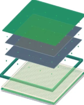
The LAPPD detector (Fig. 1.) is designed to be cheap: less than 10 $ incremental cost per inch squared. Therefore, the assembly is kept simple. It consists of four parts, from top to bottom: the photo-cathode, the MCP1, the MCP2, the anode strip-lines, enclosed in a glass box and separated by cylindrical spacers. The box dimensions are 20 × 20 × 3 cm3
. For simplicity also, it comprises a reduced number of pins and no internal connections.
Fig. 1. Scheme of the LAPPD MCP detector.
The bottom anodes are readout on both sides using our custom made CMOS sampling chip.
4. Simulation work
As part of the simulation effort, a close look at the signal development and the signal propagation in the anodes as performed. This allows a better
understanding of the detector behavior, the validation of experimental re-sults and the investigation of design for better efficiency. The main tools used for simulations are HFSS c# for frequency domain simulation and Matlab c# for field simulation and plots.
4.1. Anode signal development
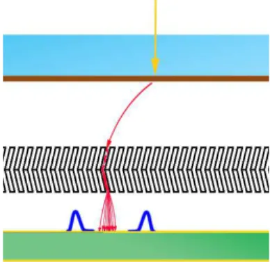
Fig. 2. illustrates the working principle of an MCP detector: an incoming photon (marked as yellow arrow) is converted into an electron (red) by a photo-cathode. Then it is accelerated in the MCPs’ channels where the signal amplification due to the secondary emissions takes place. The bottom part of the figure illustrates the signal development in the anode gap: the cloud of electrons coming out of the MCPs is being accelerated towards the anodes stripline. During this process the electromagnetic field radiated by the electrons induces on the stripline a current pulse (blue) that propagates towards both ends.
Fig. 2. Principle of electron amplification and signal development in the detector.
The simulation of the signal creation is under progress using Matlab c#. No results are yet to be reported. However, this simulation turned out to be complex due to the fact that it is: time dependent, in the near field region and in the presence of charge sources (electrons).
4.2. Anode signal propagation
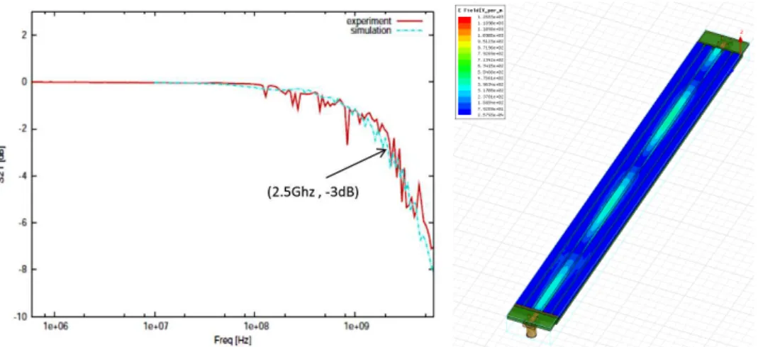
Another potentially limiting factor on the signal path is the anodes band-width. Figure 3 (left) shows a comparison between the simulated and mea-sured bandwidth of the anodes. They are in a very good agreement and give a 3 dB cutoff frequency at 2.5GHz. The model that has been used for simulation purposes is shown in the right part of the figure. The simulation has been done using HFSS c#.
38 D. Breton et al.
Fig. 3. Left: Plot of the simulation and measurement of the anode bandwidth, Right: Anode model implement in HFSS for bandwidth simulation, here plot of the field magnitude at 1 GHz.
5. Timing extraction on fast signal
Many techniques are available in order to extract the time-of-arrival of the pulses coming from the detector. Four of them are displayed in Fig. 4.
Fig. 4. Simple sketches comparing the timing extraction for four different tech-niques: single threshold, multiple threshold, constant fraction and sampling.
The threshold methods (two upper plots), with advantage of simplicity, poorly correct both the noise and non-linearity, therefore frequently yield-ing a bad timyield-ing. The constant fraction method does not present these inconveniences but it is hard to be implemented in chip. The fourth, signal sampling, provided it is done above the Shannon frequency of the signal, fully preserves its integrity, thus its timing. It is also possible to use a higher sampling frequency allowing for a better signal reconstruction and noise suppression.
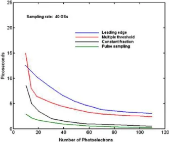
Figure 5 illustrates the differences between the methods. For a high number of photo-electrons (high SNR) the constant fraction and sampling methods are almost equivalent. However, for a small number of photo-electron (small SNR), we verify that the pulse sampling methods is the one that yields better results.
Fig. 5. Comparison of four timing extraction method using Matlab — courtesy of J.F. Genat.
6. LAPPD: Development of a 10 Gs/s sampling chip 6.1. Chip specifications
In compliance with the previous studies, a chip has been developed with the specification given in Table I.
6.2. Chip architecture
In order to be able to sample at such a high sampling rate, the chip is built using the switched capacitor array scheme (D. Breton, E. Delagnes, S. Ritt, G. Varner) and the IBM 130 nm process.
40 D. Breton et al.
TABLE I Main features of Multi-Anode PMTs, Silicon Photo-Multipliers, and Micro-Channel Plates.
Chip characteristics Value Technology IBM CMOS 130 nm Sampling frequency >10 Gs/s Number of channels 4 Number of sampling cells 256 Input bandwidth >2 Ghz Dead time 2 µs Number of bits 12 Power consumption 200 mW
The top level scheme of the chip is given in Fig. 6. The chip consists of a timing generator, sending high speed control signals to an array of switched capacitor array which store the input line value. Once the signal is acquired, the digitisation is done on the chip using the Wilkinson ADC. Then the data are serially sent outside.
Fig. 6. Chip internal architecture.
7. Conclusion
We are in the second year of LAPPD project funding and most of the work has not reached maturity stage yet. Unfortunately, only few results can be shown at the time of this Workshop but so far no unsurmountable obstacles have been spotted. After some delays, the chip has been fabricated and is now in the testing phase. We are expecting more results to come.