HAL Id: cea-01586412
https://hal-cea.archives-ouvertes.fr/cea-01586412
Submitted on 12 Sep 2017
HAL is a multi-disciplinary open access
archive for the deposit and dissemination of
sci-entific research documents, whether they are
pub-lished or not. The documents may come from
teaching and research institutions in France or
abroad, or from public or private research centers.
L’archive ouverte pluridisciplinaire HAL, est
destinée au dépôt et à la diffusion de documents
scientifiques de niveau recherche, publiés ou non,
émanant des établissements d’enseignement et de
recherche français ou étrangers, des laboratoires
publics ou privés.
Advanced characterizations of fluorine-free tungsten film
and its application as low resistance liner for PCRAM
Philippe Rodriguez, Romain Famulok, Yannick Le Friec, Jean-Philippe
Reynard, Benoit-Noël Bozon, Flore Boyer, Karen Dabertrand, Carine Jahan,
Sylvie Favier, Yann Mazel, et al.
To cite this version:
Philippe Rodriguez, Romain Famulok, Yannick Le Friec, Jean-Philippe Reynard, Benoit-Noël Bozon,
et al.. Advanced characterizations of fluorine-free tungsten film and its application as low resistance
liner for PCRAM. Materials Science in Semiconductor Processing, Elsevier, 2017, 71, pp.433 - 440.
�10.1016/j.mssp.2017.08.033�. �cea-01586412�
Contents lists available atScienceDirect
Materials Science in Semiconductor Processing
journal homepage:www.elsevier.com/locate/mssp
Advanced characterizations of
fluorine-free tungsten film and its application
as low resistance liner for PCRAM
Ph. Rodriguez
a,b,⁎, R. Famulok
a,b, Y. Le Friec
c, J.-Ph. Reynard
c, B.-N. Bozon
d, F. Boyer
a,b,c,
K. Dabertrand
c, C. Jahan
a,b, S. Favier
a,b, Y. Mazel
a,b, B. Previtali
a,b, P. Gergaud
a,b, F. Nemouchi
a,baUniv. Grenoble Alpes, F-38000 Grenoble, France bCEA, LETI, MINATEC Campus, F-38054 Grenoble, France
cSTMicroelectronics, 850 rue Jean Monnet, BP 16, 38926 Crolles, France dApplied Materials France, 864 chemin des Fontaines, 38190 Bernin, France
A R T I C L E I N F O
Keywords: Tungsten Contact Interconnects Liner Low resistance PCRAMA B S T R A C T
Using a metal-organic tungsten based precursor, afluorine-free tungsten thin film has been obtained. The process deposition recipe includes a plasma-enhanced CVD (PECVD) step and atomic layer deposition (ALD) cycles. A set of physicochemical characterizations including X-ray reflectivity (XRR), in-plane X-ray diffraction (XRD), wavelength dispersive X-rayfluorescence (WDXRF), plasma profiling time of flight mass spectrometry (PPTOFMS) and microscope observations has been realized in order to study the W thinfilm structure and properties. Thefilm is perfectly conformal whatever the structure size investigated (from tens of nanometers to micrometers wide). It was also highlighted that the F-free Wfilm exhibits the lowest electrical resistivity phase (α-W) but is not pure. Indeed, in addition to a top surface oxidation, a layer located at the Wfilm / substrate interface is present. This interface layer (IL) contains impurities, including carbon and oxygen, due to ligand decomposition. This IL might be deposited during the soak step or during the PECVD step.
The W liner with thicknesses ranging from 3 to 4 nm has been implemented on PCRAM structures in order to evaluate its impact on contact plug resistivity. First electrical results are promising and demonstrate the interest of using a F-free low resistance W liner. At the aspect ratio studied, the gain in terms of contact plug resistivity is about 20% compared to the process of reference using a TiN liner. Modeling shows that this benefit is mainly due to the reduction of interface resistances.
1. Introduction
Currently, interconnect technology is widely dominated by copper metallization. The conventional plug is made of TaN barrier / Ta liner /
Cu seed layer (Physical Vapor Deposition, PVD) / Cu fill
(Electrochemical Deposition, ECD). Nevertheless, as feature sizes de-crease for advanced technologies, efficient copper metallization and interconnect reliability are becoming real challenges for future manu-facturing. Since for line width below 30 nm a dramatic increase of the wire resistance is observed, many metallization schemes are currently under development[1–3].
Various options are investigated: (i) using Cu, new barrier and liner combinations are being investigated and (ii) Cufill replacing by alter-native metals is also studied. For instance, Co and Ru liners have been proposed in order to improve damascene Cu gap-fill[4,5]and the use of Mn-based barrier has been demonstrated to reduce line resistance[6]. Filling via with Co without any barrier promises resistance and/or yield
benefit at around 15 nm via CD[7]. Ruthenium is also studied as an alternative metallization for future technology nodes with wire widths of 10 nm and below[8,9].
In parallel to Cu metallization, tungsten plug processes have been widely used in the most advanced semiconductor devices[10,11]. Due to his low resistivity and conformal bulkfill in high aspect ratio and narrow features, W metallization is a serious alternative to the Cu one. Cu suffers from different shortcomings. As described previously, the first one is the resistivity size effect, namely, the rise in electrical re-sistivity when sample structural dimensions (thicknesses in case of films, line heights and widths in case of interconnects) are reduced. This is linked to its relatively large electron mean free path (EMFP) of 39 nm at room temperature[12–15]. On the other hand, the upper limit to the EMFP of W has been reported as 10 nm[16]. Therefore, even if the room-temperature bulk resistivity of W at 5.3 μΩ.cm is more than three times higher than for Cu at 1.7 μΩ.cm, the resistivity of W is predicted to cross below that for Cu at linewidths below 25 nm[17]. In addition, the
http://dx.doi.org/10.1016/j.mssp.2017.08.033
Received 19 July 2017; Accepted 27 August 2017
⁎Corresponding author at: Univ. Grenoble Alpes, F-38000 Grenoble, France.
E-mail address:philippe.rodriguez@cea.fr(P. Rodriguez).
1369-8001/ © 2017 Elsevier Ltd. All rights reserved.
second shortcoming is the degraded reliability of Cu as device operating temperatures and current densities increase with each technology node. Electromigration is the main factor to explain the reliability issues [18–20]. The higher melting temperature of tungsten (more than twice of copper) should result in improved interconnect reliability, qualita-tively similar to the improvement observed when Cu was introduced to replace Al interconnects[21].
In tungsten plug process, the traditional metallization has used the sequential following scheme: TiN /SiH4orB H2 6 nucleation layers / WF6CVD W, where the TiN (3–5 nm) acts as both an adhesion layer on dielectrics and a barrier to F dissemination during the CVD W process. The nucleation layer (2–3 nm) serves as a nucleation layer for the low resistance CVD W. This conventional process may no longer be ex-tendable to high aspect-ratio small contact holes. Indeed, for a 10–15 nm contact hole all the volume will be occupied by the barrier and the nucleation layer. This phenomenon is evidenced for a 12 nm contact hole onFig. 1. The major challenge for Wfill scaling is thus to improve the line Rs and Rcby increasing the volume of the low re-sistance CVD W bulk material. So far, TiN has been the best known material to provide an adhesion layer for CVD W and to restrain fluorine diffusion but a nucleation layer is then required before CVD W. Fluorine-free tungstenfilm has been recently suggested as an ideal so-lution to substitute the high resistance TiN andB H2 6nucleation layer [22,23].
In this work, by using a metal-organic tungsten based precursor, a fluorine-free tungsten thin film has been obtained using plasma-en-hanced CVD step and ALD cycles. The structure and properties of the tungsten thin film have been studied using a set of physicochemical characterizations. Finally, the low resistance W liner has been im-plemented on PCRAM structures in order to evaluate its impact on contact plug resistivity.
2. Experimental details
A Volta™ CVD W chamber has been installed on a 300 mm Applied Materials Endura platform. This chamber enables afluorine-free tung-sten deposition. Deposition temperature is set at180 C. The sequence° used for this study consists in a first step of precursor soak, then a plasma-enhanced CVD (PECVD) step is performed andfinally atomic layer deposition (ALD) cycles are realized. The soak and PECVD steps lead to afilm thickness of about 1 nm (XRR measurement); the desired thickness is then modulated by the number of ALD cycles. Argon is used as carrier gas and a metal-organic tungsten compound provided by Entegris under the name Joppa27™ is used as tungsten precursor. Regarding the safety data sheet, this latter compound is doubtless based on tungsten carbonyl W(CO)6. During the ALD process, Ar/H2plasma is used as a counter-reactant to reduce primary species into W film. In order to isolate the Wfilms from the Si(100) substrate, all depositions have been realized on a 100 nm thick thermal silicon oxide (except for
WDXRF analyses where Wfilms were directly deposited on Si). The sheet resistance of samples was measured by using a fully au-tomatic 4 point probe sheet resistance Napson WS-3000 tool, X-ray reflectivity (XRR) spectra were acquired on a Jordan Valley JVX5200 X-ray reflectometer, in plane X-X-ray diffraction (XRD) was performed on Rigaku SmartLab high-resolution X-ray diffractometer, depth profiling was achieved using a Horiba Jobin Yvon Plasma Profiling Time Of Flight Mass Spectrometry (PPTOFMS) instrument and Wavelength Dispersive X-ray Fluorescence (WDXRF) was realized on Rigaku AZX400 sequential WDXRF spectrometer. Hitachi S-5500 scanning electron microscope (SEM) was used to observe conformality of tung-sten films in contact plugs. For PCRAM structures, additional trans-mission electron microscopy (TEM) observations were performed and contact plug resistivity was evaluated using a 2-wire resistance test on a chain of contacts.
3. Results and discussion
3.1. Physicochemical characterization of tungstenfilms
The resistivity of F-free W (solid circles) films as a function of thickness in the as-deposited state has been plotted on Fig. 2. For comparison, values obtained for TiNfilm (open circles) traditionally used as adhesion layer and F barrier have been added. This figure clearly exhibits the possible gain in resistivity by using F-free tungsten as low resistance liner instead of the classical TiN material. Indeed, for thickness ranging between 3 and 5 nm (e.g. the standard thickness for TiN liner) the resistivity of the W liner is at least 60% lower than the one of TiN (around 200 μΩ.cm for Wfilm vs. 600 μΩ.cm for TiN). Even for higher thicknesses (15– 40 nm), the resistivity of TiN films remains greater than the one of thinner Wfilms.
Since thinfilms of tungsten can be deposited either as an equili-brium phase with a body-centered-cubic structure denotedα-W of low electrical resistivity or as a metastable phase with an A15 (cubic) structure with high values of resistivity (denoted β-W) [24,17], the crystallographic phases of the F-free tungstenfilm have been studied by X-ray diffraction (XRD) measurements. TheFig. 3shows the in-plane XRD pattern obtained for a 10 nm thick F-free Wfilm. The inset table reproduces the calculated lattice parameter for each diffraction peak identified.
In the 2 θ range 30–100°, 3 diffraction peaks can be distinguished. Thanks to a modeling of the experimental spectrum, these peaks have all been attributed to the tungstenα-phase. The peak located at 38.7° matches with the {1 1 0} planes while peaks located at 69.7° and 82.1° correspond to {2 1 1} and {2 2 0} planes, respectively. Thus, the as-deposited F-free Wfilm exhibits the lowest electrical resistivity phase:
α-W. The calculated lattice parameter (from experimental data) is about
Fig. 1. Schematic representation of conventional tungsten plug process and the use of F-free W liner for a 12 nm contact hole.
Fig. 2. Resistivity of F-free W (solid circles) and TiNfilms (open circles) as a function of thickness in the as-deposited state.
P. Rodriguez et al. Materials Science in Semiconductor Processing 71 (2017) 433–440
3.30Å whereas the bulk one is 3.16 Å. Therefore, impurities are probably present within thefilm.
Thanks to XRR and sheet resistance analyses, the evolution of the F-free Wfilm in terms of thickness and resistance has been followed, this latter is depicted onFig. 4.
Once thefilm is vented to the atmosphere, a fast increase of the thickness has been observed in thefirst hours. Indeed, in the first seven hours, the initial thickness measured at around 3.3 nm increased to 3.4 nm. Then, thefilm thickness tends to stabilize. This trend is corre-lated with a concomitant increase of the sheet resistance in the first hours of about 15Ω/□. These phenomena have been related to a fast oxidation of the F-free Wfilms and are consistent with the XRR mod-elings obtained in this study which systematically exhibit the presence of aWOxtop surface layer.
X-ray reflectivity (XRR) analyses have been performed and the modeling of the experimental spectra has been realized in order to obtain the thickness and the electronic density of the layers present in the samples. The Fig. 5 exhibits the XRR spectrum and the corre-sponding modeling obtained for a 9 nm thick F-free Wfilm. The inset table reproduces the thickness and the density of the modeled layers.
The XRR analyses demonstrate the presence of a W layer of 5.1 nm thick with a density of 18.1 g/cm3. On the top of this layer, a 3.1 nm thick layer with a density of 12.6 g/cm3has been related to a tungsten oxide layer and labeled WOx. Moreover, in order to obtain a good modeling, an interface layer (IL) of about 1 nm thick has been added. This IL might be related (i) to the deposition of precursor during the soak step or (ii) to the incomplete decomposition of the tungsten pre-cursor during the PECVD step.
In order to support the latter assumption and to identify the nature of the interface layer, additional characterizations have been realized. First, Wavelength Dispersive X-ray Fluorescence (WDXRF) analyses
have been performed on Si wafer: (i) just after a 10 nm thick F-free tungsten film deposition and (ii) on a reference Si wafer (Si wafer without any deposition). This latter is used as a control wafer in order to have a baseline of clean room atmosphere impact. TheFig. 6displays the results obtained for tungsten, carbon and oxygen lines. A Tifilter has been used for W line analyses in order to prevent the diffraction of the Si substrate.
Obviously, no W is detected on reference Si wafer whereas a strong emission corresponding to the WLαline is detected on F-free Wfilm. From the analysis of C and O lines, it has been demonstrated that the carbon and oxygen content are significantly higher for F-free W films than for reference Si wafer. Indeed, the carbon line intensity for F-free Wfilm is nearly 6 times higher than for the reference wafer whereas the oxygen line intensity is 2.8 times higher. This observation is in good accordance with the XRD results: F-free W is not pure and C and O impurities are present.
If the WDXRF analyses confirm the presence of C and O impurities, this kind of analysis is realized on the wholefilm volume. In order to spatially localize these impurities, Plasma Profiling Time Of Flight Mass Spectrometry (PPTOFMS) analyses were performed. TheFig. 7depicts the depth profile for a 4 nm thick F-free W film using the PPTOFMS analysis technique.
On the sample surface, oxygen, carbon and silicon are present. Carbon is probably related to surface contamination whereas oxygen is linked to the Wfilm oxidation. Silicon presence on the sample surface is due to the analysis chamber conditioning. The depth profile exhibits the presence of carbon at the Wfilm /SiO2interface. This latter cannot be related to contamination becauseSiO2/Si wafers are in situ cleaned before Wfilm deposition. Thus, PPTOFMS analyses comfort the XRR modeling: at the Wfilm /SiO2interface, a layer is present and this latter contains a high percentage of carbon.
Thanks to the combination of various physicochemical character-izations, the nature and the organization of the F-free Wfilm has been defined. The W layer is made ofα-W, the lowest electrical resistivity phase. Once thefilm is vented to the atmosphere, a fast surface oxi-dation occurs and aWOxlayer appears. A layer located at the Wfilm / substrate interface has also been evidenced. This interface layer (IL) contains impurities, including C and O, due to ligand decomposition. It might be deposited during the soak step or during the PECVD step. Regarding the nature of the metal-organic tungsten based precursor, the IL composition can be related to a W(CO)x layer. A schematic re-presentation of the F-free Wfilm is given onFig. 8.
Finally, the conformality of the tungstenfilms has been studied in various structures by SEM observations. Typical examples of the results obtained are shown inFig. 9.
As illustrated by the top SEM picture inFig. 9, the Wfilm is perfectly conformal. Indeed, the film fully covers the sides of the contact
Fig. 3. In-plane X-ray diffraction pattern of F-free W (10 nm) / SiO2(100 nm) / Si sample.
Fig. 4. Study of thefilm aging: evolution of thickness and sheet resistance.
Fig. 5. X-ray reflectivity spectrum and modeling obtained for a F-free W (9 nm) / SiO2
structure– even in the case of the presence of etching defects – which is essential for its role of barrier to F diffusion and nucleation layer. Whatever the structure size studied (from tens of nanometers to mi-crometers wide), the tungsten film is absolutely conformal and its thickness is quite uniform.
3.2. PCRAM applications
In embedded PCRAM technology, as the PCM module is integrated between the front-end and the back-end of the CMOS process, the compatibility of the memory integration with the advanced CMOS process must be carefully evaluated. A thicker pre-metal dielectric is needed to allocate the storage element in the PCRAM structure and a stacked contact becomes mandatory everywhere in the circuitry. However a higher resistive stacked contact could be detrimental to the
Fig. 6. Wavelength Dispersive X-ray Fluorescence analyses of a F-free Wfilm and a re-ference Si wafer: W line (top), C line (middle) and O line (bottom).
Fig. 7. Depth profile of a F-free W (4 nm) / SiO2(100 nm) / Si sample using PPTOFMS.
Fig. 8. Schematic representation of a F-free Wfilm based on physicochemical char-acterizations realized in this study.
Fig. 9. SEM observations of two contact structures cross section after F-free Wfilm de-position. Due to the contrast used, the Wfilm appears in bright on these SEM pictures. P. Rodriguez et al. Materials Science in Semiconductor Processing 71 (2017) 433–440
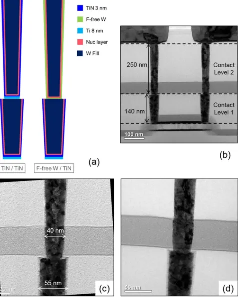
CMOS baseline performances. The F-free W liner has been implemented on PCRAM architecture in order to evaluate its impact on contact plug resistivity. In addition to the PCM structures containing the phase change material and MOS selectors, contact chains frameworks are available to evaluate the stacked contact resistance. These latter are made of a two level stacked contact plugs: the normal contact corre-sponds to the level 1 and the secondary contact is on the level 2. A schematic representation of these stacked contact plugs are shown on Fig. 10(a) and a TEM image of a complete stacked contact plug is given onFig. 10(b).
The contact level 1 is 140 nm high and 55 nm wide whereas the contact level 2 is 250 nm high and 40 nm wide. For the process of re-ference (POR), whatever the contact level, the metallization process is the following: a 8 nm thick Ti layer is deposited in the contact plug's bottom, then a 3 nm thick TiN liner covers the sides of the plug and a nucleation layer is realized before the Wfilling. For the samples using the F-free W liner, the latter has only been implemented in substitution of the TiN liner on contact level 2, nucleation layer has been kept but the Ti layer was removed. Contact level 1 remains unchanged. These two configurations are illustrated on theFig. 10(a) and high magni fi-cation TEM images have been realized for each process: theFig. 10(c) corresponds to the POR whereas theFig. 10(d) shows the process with the F-free W liner.
Using a 2-wire resistance test, electrical results have been obtained for the POR and the process implementing the W liner. TheFig. 11
displays the cumulative distribution functions (CDF) obtained for the contact plug line resistance of PCRAM structures using the POR or the F-free W liner process.
The comparison of the line resistance obtained for 2 different structures using the POR highlights that between two comparable processes the difference in terms of line resistance is about 2–2.5%. This discrepancy might be attributed to slight process variations from a
Fig. 10. (a) Schematic representation of the stacked contact plugs for the process of reference (left) and the process implementing the F-free W liner (right), (b) TEM image of a complete stacked contact plug, (c) TEM image for a stacked contact plug with the process of reference, (d) TEM image for a stacked contact plug with the F-free W liner on level 2.
Fig. 11. Cumulative distribution functions obtained for contact plug line resistance of PCRAM structures using the process of reference or the F-free W liner process.
structure to another and/or to the measurement error linked to the 2-wire resistance test. Nevertheless, the slight difference obtained for the structures using the POR especially underlines the fact that the varia-tion obtained in terms of line resistance when using the F-free W liner is unquestionably significant. Indeed, at constant liner thickness (e.g. 3 nm), line resistance benefit from switching from TiN-based to W-based metallization is up to 23%. Moreover, using W liner, the line resistance distribution appears to be narrower. As a matter of fact, the ratio between the standard deviation value for POR and the one for W liner process is up to 1.7. Therefore, using W liner not only leads to a significant decrease of the line resistance but also allows reducing disparities from a contact plug to another.
The influence of the W liner thickness on the line resistance benefit has been studied. Normalized contact plug resistances obtained for POR and W liner process with various thicknesses are plotted onFig. 12.
For a normalized contact plug resistance of 100 for the POR, the line resistance is 78 and 82 when using W liner with thicknesses of 3 and 4 nm, respectively. As expected, the line resistance decrease with the W liner thickness. This is related to an increase of the low resistance CVD Wfill volume. However, what is remarkable is that even with a W liner thickness (4 nm) greater than the TiN one in the POR (3 nm), the line resistance reduction is still meaningful. These encouraging results might be explained by a combination of various factors: the lowest resistivity of the W liner compared to the one of TiN is a first ex-planation but it is probably not the only one. The interface resistances are believed to be predominant in this kind of system. By changing the nature of the liner, the interface resistances between the liner and the nucleation layer, the liner and the contact level 1, the liner and the top metal are modified. Thus, the substitution of TiN by W should lead to reduce these interface resistances and decrease the overall line re-sistance of the contact plugs.
3.3. Modeling of resistances of the contact plug
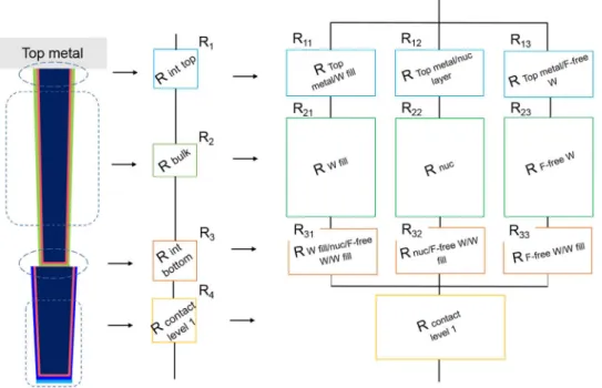
In order to explain the relative high gain in contact resistance ob-tained by substituting the classical TiN metallization by the F-free W one, the stacked contact plug has been modeled using four resistors in series (seeFig. 13). Thefirst one (Rint top,R1) models the top interface between the top metal and the contact level 2, the second one (Rbulk, R2) represents the bulk resistance of the contact plug, the third one (Rint bottom, R3) reproduces the interface between the bottom of the contact level 2 and the top of the contact level 1 and the fourth resistor (Rcontact level 1,R4) models the total resistance of contact level 1.
According to Eq.(1), the total resistanceRTotalis the sum of the four resistors in series.
= + + +
RTotal R1 R2 R3 R4 (1)
Rint top, Rbulk and Rint bottom contain concentric layers of different materials, parallel to the current path. Therefore, it is possible to de-compose each of these series resistance in 3 parallel resistances, as follow.
Each resistor in series contains concentric layers of different mate-rials, parallel to the current path. Therefore, each of the resistors in series is also divided into various resistors in parallel as follow:
= + + R R R R 1 1 1 1 1 11 12 13 (2) = + + R R R R 1 1 1 1 2 21 22 23 (3) = + + R R R R 1 1 1 1 3 31 32 33 (4)
In order to deduce the contribution of the interfaces in the total resistance, one can chose to calculate the contribution of the bulk Rbulk and compare the latter to the total resistance. To do so, the bulk part of the structure was considered to be a perfect cylinder containing con-centric layers of different materials. The general equation used to de-duce the resistance value of a specific layer is given by Eq.(5).
= R ρ L
S .
(5) With ρ (Ω.mm) the given material resistivity, L (mm) the material bulk length, and S (mm2) the area of the material perpendicular to the current path.
In this model, only the main path of the current has been taking into account. For example, parasitic resistances between adjacent layers like resistance between W Fill and nucleation layer or resistance between nucleation layer and TiN or F-free W liner have been neglected.
Knowing the resistivity of the different materials involved in the stacked contact plug and the total resistance of contact level 1, the contribution of each resistor in contact level 2 has been evaluated. Due to a lower resistivity of the F-free W liner compared to the classical TiN liner (seeFig. 2), the bulk resistance of the contact level 2 (Rbulk on Fig. 13) is slightly lower when the integration involved the F-free W liner. Nevertheless, the difference is minimal and cannot explained the benefit measured for the line resistance of PCRAM contact. It appears that the benefit in terms of contact plug resistance is governed by the reduction of interface resistances and that the contribution induced by the reduction of the bulk resistivity is secondary. Indeed, for the POR, the interface resistances represent 52.7% of the total contact plug re-sistance for the contact level 2. These interface rere-sistances fail at 28.4% for the process using F-free W liner.
4. Conclusion
By combining the various characterization techniques involved in this study, we obtained valuable information on physicochemical characteristics of fluorine-free tungsten film. This latter is perfectly conformal whatever the structure size investigated. We have also highlighted that the F-free Wfilm is not pure. In addition to a surface oxidation, an interface layer is present between the W film and the substrate. This interface layer is probably made of W(CO)xand might be related (i) to the deposition of precursor during the soak step or (ii) to the incomplete decomposition of the precursor during the PECVD step.
Flurorine-free tungstenfilm has been successfully implemented on PCRAM structures. By substituting the conventional TiN liner by this W liner, the line resistance of PCRAM contact plugs has been decreased of about 20%. This benefit has been linked, by modeling, to the reduction of interface resistances when using the F-free W liner.
Thesefirst results are encouraging and confirm the strong interest of using F-free W liner for this kind of contact structure. Contrary to ex-pectations, the F-free W liner is not only valuable in very small feature
Fig. 12. Influence of W liner thickness on line resistance gain.
P. Rodriguez et al. Materials Science in Semiconductor Processing 71 (2017) 433–440
but also in larger plugs mainly due to its interface resistance im-provement. Thus, beyond PCRAM, others applications in logic, power or photonics may benefit from such films.
Acknowledgments
This research was supported by the French National Research Agency (ANR) under the“Investissements d′avenir” programs:
ANR-11-EQPX-0010, FDSOI11 and IRT Nanoelec’ ANR-10-AIRT-05, by
Nano2017 project and by STMicroelectronics - CEA LETI alliance pro-gram.
References
[1] L. Carbonell, H. Volders, N. Heylen, K. Kellens, R. Caluwaerts, K. Devriendt, E.A. Sanchez, J. Wouters, V. Gravey, K. Shah, Q. Luo, A. Sundarrajan, J. Lu, J. Aubuchon, P. Ma, M. Narasimhan, A. Cockburn, Z. Tökei, G.P. Beyer, Metallization of sub-30 nm interconnects: Comparison of different liner/seed combinations, in: Proceedings of the 2009 IEEE International Interconnect Technology Conference, 2009, pp. 200–202.http://dx.doi.org/10.1109/IITC.2009.5090387.
[2] N. Jourdan, L. Carbonell, N. Heylen, J. Swerts, S. Armini, A.M. Caro, S. Demuynck, K. Croes, G. Beyer, Z. Tökei, S.V. Elshocht, E. Vancoille, Evaluation of metallization options for advanced Cu interconnects application, ECS Trans. 34 (1) (2011) 515–521.
[3] Z. Tökei, End of Cu roadmap and beyond Cu, in: Proceedings of the 2016 IEEE International Interconnect Technology Conference / Advanced Metallization Conference (IITC/AMC), 2016, pp. 1–58.http://dx.doi.org/10.1109/IITC-AMC. 2016.7507738.
[4] T. Nogami, M. He, X. Zhang, K. Tanwar, R. Patlolla, J. Kelly, D. Rath, M. Krishnan, X. Lin, O. Straten, H. Shobha, J. Li, A. Madan, P. Flaitz, C. Parks, C.K. Hu, C. Penny, A. Simon, T. Bolom, J. Maniscalco, D. Canaperi, T. Spooner, D. Edelstein, CVD-Co/ Cu(Mn) integration and reliability for 10 nm node, in: Proceedings of the 2013 IEEE International Interconnect Technology Conference, 2013, pp. 1–3.http://dx.doi. org/10.1109/IITC.2013.6615592.
[5] R.H. Kim, B.H. Kim, J.N. Kim, J.J. Lee, J.M. Baek, J.H. Hwang, J. Hwang, J. Chang, S.Y. Yoo, T.J. Yim, K.M. Chung, K.H. Park, T. Oszinda, I.S. Kim, E.B. Lee, S.D. Nam, S. Jung, Y.W. Cho, H.J. Choi, J.S. Kim, S.H. Ahn, S.H. Park, B.U. Yoon, J.H. Ku, S.S. Paak, N.I. Lee, S. Choi, H.K. Kang, E.S. Jung, High performance Cu/low-k inter-connect strategy beyond 10 nm logic technology, in: Proceedings of the 2015 IEEE International Interconnect Technology Conference and 2015 IEEE Materials for Advanced Metallization Conference (IITC/MAM), 2015, pp. 1–4.http://dx.doi.org/ 10.1109/IITC-MAM.2015.7325599.
[6] Y.K. Siew, N. Jourdan, Y. Barbarin, J. Machillot, S. Demuynck, K. Croes, J. Tseng, H. Ai, J. Tang, M. Naik, P. Wang, M. Narasimhan, M. Abraham, A. Cockburn, J. Bömmels, Z. Tökei, CVD Mn-based self-formed barrier for advanced interconnect technology, in: Proceedings of the 2013 IEEE International Interconnect Technology Conference, 2013, pp. 1–3.http://dx.doi.org/10.1109/IITC.2013.6615551. [7] M.H. van der Veen, K. Vandersmissen, D. Dictus, S. Demuynck, R. Liu, X. Bin, P.
Nalla, A. Lesniewska, L. Hall, K. Croes, L. Zhao, J. Bömmels, A. Kolics, Z. Tökei, Cobalt bottom-up contact and via prefill enabling advanced logic and DRAM
technologies, in: Proceedings of the 2015 IEEE International Interconnect Technology Conference and 2015 IEEE Materials for Advanced Metallization Conference (IITC/MAM), 2015, pp. 25–28.http://dx.doi.org/10.1109/IITC-MAM. 2015.7325605〉.
[8] J. Swerts, Y.-K. Siew, E.V. Besien, Y. Barbarin, K. Opsomer, J. Bömmels, Z. Tökei, S.V. Elshocht, Scalability of RuTiN barriers deposited by plasma-enhanced atomic layer deposition for advanced interconnects, Microelectron. Eng. 120 (2014) 235–239,http://dx.doi.org/10.1016/j.mee.2013.08.008.
[9] L.G. Wen, P. Roussel, O.V. Pedreira, B. Briggs, B. Groven, S. Dutta, M.I. Popovici, N. Heylen, I. Ciofi, K. Vanstreels, F.W. Østerberg, O. Hansen, D.H. Petersen, K. Opsomer, C. Detavernier, C.J. Wilson, S.V. Elshocht, K. Croes, J. Bömmels, Z. Tökei, C. Adelmann, Atomic layer deposition of ruthenium with TiN interface for sub-10 nm advanced interconnects beyond copper, ACS Appl. Mater. Interfaces 8 (39) (2016) 26119–26125,http://dx.doi.org/10.1021/acsami.6b07181. [10] P. Ireland, High aspect ratio contacts: A review of the current tungsten plug process,
Thin Solid Films 304 (1) (1997) 1–12,http://dx.doi.org/10.1016/S0040-6090(96) 09557-0.
[11] T. Luoh, C.-T. Su, T.-H. Yang, K.-C. Chen, C.-Y. Lu, Advanced tungsten plug process for beyond nanometer technology, Microelectron. Eng. 85 (8) (2008) 1739–1747,
http://dx.doi.org/10.1016/j.mee.2008.04.030.
[12] F. Chen, D. Gardner, Influence of line dimensions on the resistance of Cu inter-connections, IEEE Electron Device Lett. 19 (12) (1998) 508–510,http://dx.doi.org/ 10.1109/55.735762.
[13] T. Sun, B. Yao, A.P. Warren, V. Kumar, S. Roberts, K. Barmak, K.R. Coffey, Classical size effect in oxide-encapsulated Cu thin films: Impact of grain boundaries versus surfaces on resistivity, J. Vac. Sci. Technol. A 26 (4) (2008) 605–609,http://dx.doi. org/10.1116/1.2938395.
[14] T. Sun, B. Yao, A.P. Warren, K. Barmak, M.F. Toney, R.E. Peale, K.R. Coffey, Dominant role of grain boundary scattering in the resistivity of nanometric Cufilms, Phys. Rev. B 79 (2009) 041402,http://dx.doi.org/10.1103/PhysRevB.79.041402. [15] T. Sun, B. Yao, A.P. Warren, K. Barmak, M.F. Toney, R.E. Peale, K.R. Coffey, Surface
and grain-boundary scattering in nanometric Cufilms, Phys. Rev. B 81 (2010) 155454,http://dx.doi.org/10.1103/PhysRevB.81.155454.
[16] S.M. Rossnagel, I.C. Noyan, C. Cabral Jr., Phase transformation of thin sputter-de-posited tungstenfilms at room temperature, J. Vac. Sci. Technol. B 20 (5) (2002) 2047–2051,http://dx.doi.org/10.1116/1.1506905.
[17] D. Choi, B. Wang, S. Chung, X. Liu, A. Darbal, A. Wise, N.T. Nuhfer, K. Barmak, A.P. Warren, K.R. Coffey, M.F. Toney, Phase, grain structure, stress, and resistivity of sputter-deposited tungstenfilms, J. Vac. Sci. Technol. A 29 (5) (2011) 051512,
http://dx.doi.org/10.1116/1.3622619.
[18] C.-K. Hu, B. Luther, F. Kaufman, J. Hummel, C. Uzoh, D. Pearson, Copper inter-connection integration and reliability, Thin Solid Films 262 (1) (1995) 84–92,
http://dx.doi.org/10.1016/0040-6090(94)05807-5.
[19] C.-K. Hu, J. Harper, Copper interconnections and reliability, Mater. Chem. Phys. 52 (1) (1998) 5–16,http://dx.doi.org/10.1016/S0254-0584(98)80000-X.
[20] B. Li, T.D. Sullivan, T.C. Lee, D. Badami, Reliability challenges for copper inter-connects, Microelectron. Reliab. 44 (3) (2004) 365–380,http://dx.doi.org/10. 1016/j.microrel.2003.11.004.
[21] C.S. Hau-Riege, An introduction to Cu electromigration, Microelectron. Reliab. 44 (2) (2004) 195–205,http://dx.doi.org/10.1016/j.microrel.2003.10.020. [22] J. Bakke, Y. Lei, Y. Xu, K. Daito, X. Fu, G. Jian, K. Wu, R. Hung, R. Jakkaraju, N.
Breil, Fluorine-free tungstenfilms as low resistance liners for tungsten fill appli-cations, in: Proceedings of the 2016 IEEE International Interconnect Technology Conference / Advanced Metallization Conference (IITC/AMC), 2016, pp. 108–110.
Fig. 13. Modeling of resistances present in the con-tact plug of the level 2.
〈http://dx.doi.org/10.1109/IITC-AMC.2016.7507699〉.
[23] X. Fu, G. Jian, J. Zhou, R. Jakkaraju, N. Yoshida, P. Ma, A conformal low resistivity fluorine free tungsten for FinFET metal gate and 3D memory applications, in: Proceedings of the 2016 China Semiconductor Technology International Conference (CSTIC), 2016, pp. 1–4.http://dx.doi.org/10.1109/CSTIC.2016.7464018〉.
[24] G.S. Chen, H.S. Tian, C.K. Lin, G.-S. Chen, H.Y. Lee, Phase transformation of tungstenfilms deposited by diode and inductively coupled plasma magnetron sputtering, J. Vac. Sci. Technol. A 22 (2) (2004) 281–286,http://dx.doi.org/10. 1116/1.1642651.
P. Rodriguez et al. Materials Science in Semiconductor Processing 71 (2017) 433–440