HAL Id: hal-02272351
https://hal.archives-ouvertes.fr/hal-02272351
Submitted on 2 Jul 2020HAL is a multi-disciplinary open access archive for the deposit and dissemination of sci-entific research documents, whether they are pub-lished or not. The documents may come from teaching and research institutions in France or abroad, or from public or private research centers.
L’archive ouverte pluridisciplinaire HAL, est destinée au dépôt et à la diffusion de documents scientifiques de niveau recherche, publiés ou non, émanant des établissements d’enseignement et de recherche français ou étrangers, des laboratoires publics ou privés.
Ionic Glass–Gated 2D Material–Based Phototransistor:
MoSe 2 over LaF 3 as Case Study
Ulrich Nguétchuissi Noumbé, Charlie Gréboval, Clément Livache, Thibault
Brulé, Bernard Doudin, Abdelkarim Ouerghi, Emmanuel Lhuillier,
Jean-francois Dayen
To cite this version:
Ulrich Nguétchuissi Noumbé, Charlie Gréboval, Clément Livache, Thibault Brulé, Bernard Doudin, et al.. Ionic Glass–Gated 2D Material–Based Phototransistor: MoSe 2 over LaF 3 as Case Study. Advanced Functional Materials, Wiley, 2019, 29 (33), pp.1902723. �10.1002/adfm.201902723�. �hal-02272351�
1
Ionic glass gated 2D material based phototransistor : MoSe2 over LaF3 as case study.
Ulrich Nguétchuissi Noumbé, Charlie Gréboval, Clément Livache, Thibault Brule, Bernard Doudin, Abdelkarim Ouerghi, Emmanuel Lhuillier*, Jean-Francois Dayen*.
U.N., Prof. B.D., Dr.J-F.D.
Université de Strasbourg, IPCMS-CMRS UMR 7504, 23 Rue du Loess, 67034 Strasbourg, France
E-mail: [email protected]
C.G., C.L., Dr. E.L.
Sorbonne Université, CNRS, Institut des NanoSciences de Paris, INSP, F-75005 Paris, France. E-Mail : [email protected]
Dr.A.O.
Centre de Nanosciences et de Nanotechnologies, CNRS, Université Paris-Sud, Université Paris-Saclay, C2N–Marcoussis, 91460 Marcoussis, France
Dr. T.B.
HORIBA Scientific, HORIBA France S.A.S, Avenue de la Vauve, Passage Jobin Yvon, 91120 PALAISEAU - France
Keywords: (photodetector, phototransistor, two dimensional material, ionic glass, field effect transistor)
Abstract : Modulating the carrier density of two dimensional (‘2D’) materials is pivotal to
tailor their electrical properties, with novel physical phenomena expected to occur at higher
doping level. Here, the use of ionic glass as a high capacitance gate is explored to develop 2D
material based phototransistor operated with higher carrier concentration up to 5x1013 cm-2,
using MoSe2 over LaF3 as archetypal system. Ion glass gating reveals to be a powerful
technique combining the high carrier density of electrolyte gating methods while enabling
direct optical addressability impeded with usual electrolyte technology.
The phototransistor demonstrates ION/IOFF ratio exceeding 5 decades and photoresponse
times down to 200 µs, up to two decades faster than MoSe2 phototransistors reported so far.
Carefull phototransport analysis unveils that ionic glass gating of 2D materials allows tuning
2
contribution in electron injection regime. This remarkable property results in photoresponse
that can be modulated electrostatically by more than two orders of magnitude, while at the
same time increasing the gain bandwidth product. This study demonstrates the potential of
ionic glass gating to explore novel photoconduction processes and alternative architectures of
devices.
1. Introduction
Because they combine a band gap with new optical features1 resulting from their low
dimensionality Transition Metal DiChalcogenides (TMDC) are generating a lot of interests to
revisit the 2D physics of semiconductor.2–4 The control of carrier density becomes of utmost
importance to design building block such as pn junction5,6, field effect transistor (FET) 7, light
emitting diode8 and photodetector3,9,10. Due to chalcogenides vacancy TMDC are not
behaving as intrinsic semiconductor, MoSe2 is n type while WSe2 is p type for example. Post
synthesis control of this doping is also possible thanks to hydrogenation,11 deposition of small
electron donor and acceptor molecule.12,13 All these methods however still suffer from a lack
of post fabrication tunability, and may require alternative device fabrication process such as
resist free patterning14,15. Gate control of the carrier density remains the most conventional
method to tune the carrier density at the device level.16 Two main strategies have been
proposed to gate 2D material which are conventional dielectric (typically the silica layer on the top of a silicon wafer) and electrolyte (ionic liquid, ion gel…). In the first approach, dielectric breakdown limits the maximum accumulated carrier density within the 1012 cm-2
range. The second method is of utmost interest when larger sheet density (>1013 cm-2) are
targeted.17–19 Use of electrolyte has been exploited in TMDC to develop ambipolar FET20, to
induce superconductivity21 or for the design of pn junction.22–24 An important drawback of
3
top optical excitation since it can absorb or scatter the light, and preventing its use for
optoelectronics devices and optical studies.
Some alternative to dielectric and electrolyte have been proposed and rely on ferroelectric
polymer25 and more recently on the use of ionic glasses. The Shukla’s group22 has proposed to
use borosilicate and soda-lime glasses as ionic glass media. By applying a large electric field
on such glass slide at high temperature (400 K), ions within the glass substrate can
accumulate at the sample surface leading to a gate effect. While the method can be used to
reach high carrier density above 1014 cm-2, the gate effect can only be obtained far above
room temperature. The Cui’s group28 later proposed to change these glass for LaF 3 and
demonstrated gate effect under dark condition on MoS2, while preserving the gate tunability
down to 180K circumventing the need for large electric field and high temperature imposed
by borosilicate and soda-lime glasses. However, there is no report to date on the use of ionic
glass for photodetection. Here, we explore for the first time the possibility to control the
photoresponse of a 2D material over an extended doping range with ion glass gating, using
MoSe2 flakes over LaF3 ionic glass as archetypal system. Our MoSe2/Ionic Glass
phototransistor demonstrate high and fast photoresponsivity respect to the state of the art.
Moreover, we demonstrate that ionic glass gating can be used as a knob to tune the nature of
the carrier recombination processes, while annihilating completely the traps contribution in
electron injection regime. This new functionality enables to modulate electrostatically the
magnitude of the photoresponse over more than two orders of magnitude. Surprisingly, this
change is achieved while preserving the photoresponse time, i.e, while amplifying the gain
4
2. Results and discussion
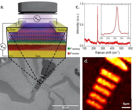
We first start by preparing a MoSe2 flake using exfoliation method and transfer it onto
the LaF3 substrate. Few layers MoSe2 flake was mechanically exfoliated from bulk crystal on
Polydimethylsiloxane (PDMS) using adhesive tapes, and then transferred onto LaF3 substrate
by dry transfer method29. The optical transparency of the LaF
3 substrate allows for simple
identification of the flakes by optical contrast. The lack of PL signal suggests that the flake is
made of multilayers MoSe2.30 This hypothesis is further confirmed by the Raman map and
spectrum, see Figure 1.c and Figure 1.d. The A1g peak of MoSe2 here appears at 242 cm-1,
while it is expected to be at 240 cm-1 for the monolayer MoSe2, confirming the multilayer
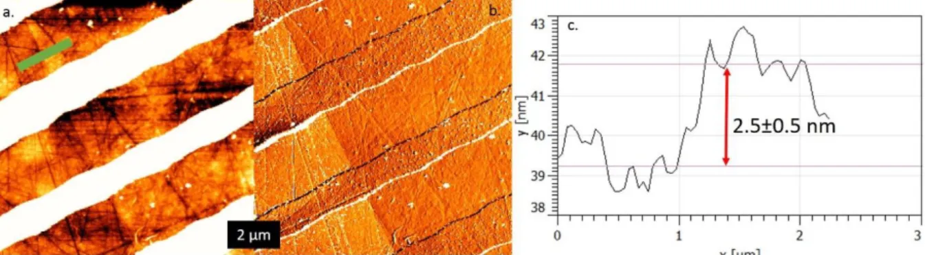
aspect of our sample. Finally using Atomic Force Microscopy, we determine the thickness of
the sample to be 2.5±0.5 nm, which correspond to 4-5 monolayers of MoSe2.
The flake is then connected to gold electrodes by electron beam lithography using a standard
bilayer PMMA (Polymethyl methacrylate) resist and an additional conductive Protective
Coating resist. A scheme of the phototransistor device as well as scanning electron
microscopy image are given in Figure 1.a-b. Finally, the sample is inserted into a cryostat for
temperature dependent phototransport study.
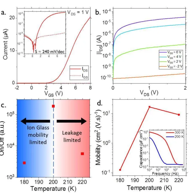
As gate bias is applied, F- vacancy moves toward or away from the surface which
induce electrostatic gating effect28. The MoSe2 flake presents a n-type characteristic which is
consistent with previous MoSe2 based FET using SiO2 as dielectric,31,32 see Figure 2a-b. It is
important to note that field effect is preserved even for operation below room temperature.
Actually we observe a maximum of the current modulation for a device temperature around
200 K, see Figure 2c. There the ION/IOFF current modulation exceeds 5 orders of magnitude
(Ion/Ioff=2x105 for VDS=0.5 V), see Figure 2b-c. Above 200 K, the On-off ratio is limited by a
5
180K, the ionic mobility of the F- vacancy gets strongly reduced and the ON current gets
lower, see Figure 2c. A subthreshold slope, defined as S=(d(logIDS)/dVGS)-1 of S≈240
mV/decade can be extracted at VDS=1V.
To have a deeper insight into the ionic glass gating mechanisms, the capacitance of LaF3 as a
function of frequency (C(f)) has been determined using an impedance meter, see Inset of
Figure 2d (see also Supporting Information and Figure S1 for technical details). At high
frequency the capacitance of the substrate is weak. At such high frequency, ions do not have
enough time to reach the surface, only the dielectric behavior of the substrate is observed.
Because the LaF3 substrate is quite thick (>1 mm), its capacitance is weak. At lower
frequency, ions get enough time to reach the surface and can form the equivalent of a ionic
double layer, and a significant rise of the capacitance is observed which now reach 1 µF.cm-2,
a value quite similar to those reported for electrolytes17. Such large capacitance allows low
gate bias operability, typically around a few volts, since carrier concentration as large as
5x1013 cm-2 are achieved under 8 V operation.
Using the C(f) curve it is now possible to estimate the field effect electronic mobility using
the expression µ𝐹𝐸 = 𝐿 𝑤𝐶𝛴𝑉𝐷𝑆
𝜕𝐼𝐷𝑆
𝜕𝑉𝐺𝑆, where L is the electrode spacing (2.6 µm), W is the
electrode length (9.3 µm), CΣ the surface capacitance taken equal to 0.1 µF.cm-2 at 200K (see
inset of Figure 2d). We found electron mobility to be µ𝐹𝐸≈ 15 cm2·V-1·s-1 at 200 K, see
Figure 2d. This value is very similar to the one reported for MoSe2 multilayer gated with
silica.32
While for TMDC the concept of dark current control using LaF3 has already been
reported28, we here extend this concept and demonstrate for the first time that the
photoresponse of 2D semiconducting material can also be tuned thanks to the ionic glass gate
6
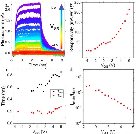
the band gap (by a 405 nm blue laser), we observe a photoconductive signal, see Figure 3a.
The magnitude of the signal can be strongly tuned using the gate bias, see Figure 3b.
Typically, the responsivity of the film reaches 50 mA/W at 0 V of gate bias and is enhanced
by a factor 4 under strong positive gate bias now exceeding 0.2 A/W. It is worth pointing that
the increase of the responsivity is not as fast as the one of the dark current. As a result the gate
bias which maximizes the signal to noise ratio is obtained under hole injection, see Figure 3d.
This regime corresponds to the one which minimizes the dark current. Rise- and fall-times
(respectively tON and tOFF in Figure 3.c) extracted from the photocurrent characteristics under
negative gate bias are close to 200 µs and 600 µs respectively. This is two orders of
magnitude faster than time responses previously reported on usual exfoliated and CVD MoSe2 10,33–37, 50 times faster than encapsulated MoSe
2 devices38, and more than one decade shorter
than the fastest MoSe2 phototransistor reported so far39. Another very striking feature comes
from the very weak gate dependence of the time response with gate bias, see Figure 3c. The
on and off time change by less than 30 % from the hole injection to the electron injection
regimes. This is remarkable since the gain bandwidth product (which can be seen as the ratio
of responsivity divided by the characteristic time constant) is actually increasing with the
applied gate. This result contrast with what is observed for phototransistor based on
nanocrystal film, 40,41 where the change of responsivity is made at quasi constant gain
bandwidth product. In other words, a higher photoresponse comes at the prize of a slower
response, on the contrary of our device.
We have then used the power dependence of the photoresponse to reveal the
recombination mechanism. While the incident power is increased, the photocurrent rises, see
Figure 4a-b. However this increase presents a sub-linear dependence and appears to be gate
tunable, see Figure 4b. Under electron injection (ie positive gate bias) the current as a
7
to the value of ½ expected for bimolecular process42,43 (ie recombination occurs through
electron hole recombination). On the other hand, under hole injection we observe an increase
of the exponent value which now reached 0.67. This value is typically intermediate between
the value of ½ expected for bimolecular process and the value of 1 obtained for
monomolecular process (ie for trapping). By applying a negative gate bias the Fermi level is
brought more deeply in the band gap and the recombination centers get unfilled and can act as
trap states, which explain the increase of the power law exponent, see the associated
mechanism in the inset of Figure 4b.
3. Conclusion
We have explored the potential of LaF3 ionic glass to build TMDC based phototransistor
with low operating bias and preserving gate tunability down to 180 K. Optimal operating
temperature is around 200K and limits the leakage through the substrate while preserving a
strong ionic mobility, with ION/IOFF ratio exceeding 5 decades. Not only the dark conductance
can be tuned but also the photoresponse which demonstrates time responses down to 200 µs,
up to two decades faster than state of the art MoSe2 phototransistors reported so far. Careful
analysis of photocurrent properties reveals that the relative contribution of traps on the carrier
recombination can be dramatically suppressed thanks to the very high accumulated carrier
concentration achieved by ion glass gating. In other words, the ion glass gate can be used as
knob to switch on and off monomolecular recombination processes. Remarkably, this novel
functionality allows for modulating the device photoresponse by more than two orders of
magnitude, while at the same time increasing its gain bandwidth product, a unique property
never observed on any other nanomaterials such as nanocrystals.
This study shows that ionic glass gate are complementary method to the usual electrolyte
8
possible when the 2D material is buried into the electrolyte gate. The performances of our
ionic glass photodetector demonstrate the potential of this method to explore novel
photoconduction processes and alternative architectures of devices. Our approach is generic,
and can be easily extended to any photoconducting nanomaterials, including organic and
molecular systems44–46, nanocrystals47,48, and hybrid materials49–54.
4. Experimental section
Device fabrication : Few layer MoSe2 was mechanically exfoliated from bulk crystal (2H
phase from graphene supermarket) on PDMS (Polydimethylsiloxane) using adhesive tapes,
and then transferred onto LaF3 substrate by dry transfer method 29. By optical contrast, we
identified the flake and, we used Ebeam lithography with a Zeiss Supra 40 scanning electron
microscope coupled to a Raith lithography system to pattern electrodes. We used a standard
bilayer PMMA (Polymethyl methacrylate) resist and a conductive Protective Coating resist
(e-spacer) to write on the insulator surface. The PMMA bilayer consists of AR-PMMA
669.04 and AR-PMMA 679.02, that were spin-coated at 4000 revolutions per minute (rpm)
during 1 min and annealed at 180 °C during 90 seconds (220nm / 4000rpm and 70nm /
4000rpm respectively). The e-spacer AR-PC 5090.02 was then spincoated at the same speed
(4000 rpm) but annealed at 90 °C during 90 seconds (90nm /4000rpm). After the development
in 1:3 MIBK-IPA at 25 °C, metal deposition Ti(3nm)/Au(47nm) was performed by electron
beam evaporator in high vacuum chamber, followed by lift-off in acetone, rinsing with
isopropanol and nitrogen jet drying.
Scanning electron microscopy : SEM is made using a FEI Magellan microscope. Images are
acquired with the e-beam accelerated with a 3 kV bias and the current from the electronic gun
set at 6 pA.
Raman and photoluminescence spectra :The micro-Raman and photoluminescence (PL)
9
micro-Raman microscope with an objective focused 532 nm and 633 nm lasers in an ambient
environment at room temperature. The excitation laser was focused onto the samples with a spot diameter of ≈0.5 µm and incident power of ≈0.1 mW. Measurements were performed on the same microscope with a 100× objective and a CCD detector (detection range from 1.2 to
6.2 eV).
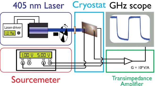
Photocurrent and electrical measurements : The sample is connected to a Keithley K2634 B
in a cryostat. It controls the applied gate voltage (VGS) and the applied drain-source bias (VDS).
The sample is illuminated by a 405 nm laser chopper at 100 Hz. A transimpedance amplifier
DLPCA-200 is added to the circuit to measure the photocurrent on a GHz oscilloscope. See
supporting information for more details, and Figure S2.
Capacitance measurements: To measure the capacitance of the sample, 80 nm of Au is
evaporated on both sides of the LaF3 substrate. It is then connected to a MFLI lock-in
amplifier that applies an AC bias of 300 mV and measures the current. See supporting
information for more details, and Figure S1.
Supporting Information
Supporting Information is available from the Wiley Online Library or from the author.
Acknowledgments
JFD thanks financial support of the Agence Nationale de la Recherche (under Labex NIE
11-LABX-0058_NIE within the Investissement d’Avenir program ANR-10-IDEX-0002-02, and
under H2DH ANR-15-CE24-0016). EL thanks the support ERC starting grant blackQD (grant
n° 756225). We acknowledge the use of clean-room facilities from the StNano platform and
the “Centrale de Proximité Paris-Centre”. We acknowledge Etienne Lorchat and Stéphane
10
Region Ile-de-France in the framework of DIM Nano-K (grant dopQD). This work was
supported by French state funds managed by the ANR within the Investissements d'Avenir
programme under reference ANR-11-IDEX-0004-02, and more specifically within the
framework of the Cluster of Excellence MATISSE and also by the grant IPER-Nano2.
References
1 K.F. Mak, C. Lee, J. Hone, J. Shan, and T.F. Heinz, Phys. Rev. Lett. 105, 136805 (2010).
2 S. Manzeli, D. Ovchinnikov, D. Pasquier, O. V. Yazyev, and A. Kis, Nat. Rev. Mater. 2,
natrevmats201733 (2017).
3 M. Long, P. Wang, H. Fang, and W. Hu, Adv. Funct. Mater. 1803807 (2018).
4 X. Duan, C. Wang, A. Pan, R. Yu, and X. Duan, Chem. Soc. Rev. 44, 8859 (2015).
5 M.S. Choi, D. Qu, D. Lee, X. Liu, K. Watanabe, T. Taniguchi, and W.J. Yoo, ACS Nano 8,
9332 (2014).
6 L. Lin, L. Liao, J. Yin, H. Peng, and Z. Liu, Nano Today 10, 701 (2015).
7 B. Radisavljevic, A. Radenovic, J. Brivio, V. Giacometti, and A. Kis, Nat. Nanotechnol. 6,
147 (2011).
8 W. Zheng, Y. Jiang, X. Hu, H. Li, Z. Zeng, X. Wang, and A. Pan, Adv. Opt. Mater. 6,
1800420 (2018).
9 O. Lopez-Sanchez, D. Lembke, M. Kayci, A. Radenovic, and A. Kis, Nat. Nanotechnol. 8,
497 (2013).
10 C. Xie, C. Mak, X. Tao, and F. Yan, Adv. Funct. Mater. 27, 1603886 (2017).
11 M.G. Silly, F. Bertran, D. Pierucci, J.E. Rault, A. Ouerghi, P. Le Fèvre, A.T.C. Johnson, H.
Henck, F. Sirotti, C.H. Naylor, A. Balan, Y.J. Dappe, and Z. Ben Aziza, ACS Nano 11, 1755
(2017).
11
H. Wang, J. Chen, N. Lu, C. Jiang, L. Li, and M. Liu, Adv. Funct. Mater. 28, 1806244 (2018).
13 S. Mouri, Y. Miyauchi, and K. Matsuda, Nano Lett. 13, 5944 (2013).
14 H.-C. Cheng, R.-J. Shiue, C.-C. Tsai, W.-H. Wang, and Y.-T. Chen, ACS Nano 5, 2051
(2011).
15 A. Mahmood, C.-S. Yang, J.-F. Dayen, S. Park, M.V. Kamalakar, D. Metten, S. Berciaud,
J.-O. Lee, and B. Doudin, Carbon N. Y. 86, 256 (2015).
16 Z.M. Wang, X. Tong, E. Ashalley, F. Lin, and H. Li, Nano-Micro Lett. 7, 203 (2015).
17 J. Lee, M.J. Panzer, Y. He, T.P. Lodge, and C.D. Frisbie, J. Am. Chem. Soc. 129, 4532
(2007).
18 J. Ye, M.F. Craciun, M. Koshino, S. Russo, S. Inoue, H. Yuan, H. Shimotani, A.F.
Morpurgo, and Y. Iwasa, Proc. Natl. Acad. Sci. U. S. A. 108, 13002 (2011).
19 H.T. Yuan, M. Toh, K. Morimoto, W. Tan, F. Wei, H. Shimotani, C. Kloc, and Y. Iwasa,
Appl. Phys. Lett. 98, 012102 (2011).
20 Y. Zhang, J. Ye, Y. Matsuhashi, and Y. Iwasa, Nano Lett. 12, 1136 (2012).
21 J.T. Ye, Y.J. Zhang, R. Akashi, M.S. Bahramy, R. Arita, and Y. Iwasa, Science 338, 1193
(2012).
22 Y.J. Zhang, J.T. Ye, Y. Yomogida, T. Takenobu, and Y. Iwasa, Nano Lett. 13, 3023 (2013).
23 H. Xu, S. Fathipour, E.W. Kinder, A.C. Seabaugh, and S.K. Fullerton-Shirey, ACS Nano 9,
4900 (2015).
24 H. Henck, D. Pierucci, J. Chaste, C.H. Naylor, J. Avila, A. Balan, M.G. Silly, M.C. Asensio,
F. Sirotti, A.T.C. Johnson, E. Lhuillier, and A. Ouerghi, Appl. Phys. Lett. 109, 113103 (2016).
25 Y. Zheng, G.-X. Ni, C.-T. Toh, C.-Y. Tan, K. Yao, and B. Özyilmaz, Phys. Rev. Lett. 105,
166602 (2010).
26 J. Biscaras, Z. Chen, A. Paradisi, and A. Shukla, Nat. Commun. 6, 8826 (2015).
27 A. Paradisi, J. Biscaras, and A. Shukla, Appl. Phys. Lett. 107, 143103 (2015).
12
29 A. Castellanos-Gomez, M. Buscema, R. Molenaar, V. Singh, L. Janssen, H.S.J. van der
Zant, and G.A. Steele, 2D Mater. 1, 011002 (2014).
30 X. Zhang, D.R.T. Zahn, J. Börner, M. Albrecht, O. Gordan, S. Michaelis de Vasconcellos,
C. Kloc, P. Tonndorf, P. Böttger, R. Bratschitsch, A. Liebig, and R. Schmidt, Opt. Express 21,
4908 (2013).
31 S. Larentis, B. Fallahazad, and E. Tutuc, Appl. Phys. Lett. 101, 223104 (2012).
32 L.D.N. Mouafo, F. Godel, G. Froehlicher, S. Berciaud, B. Doudin, M.V. Kamalakar, and
J.-F. Dayen, 2D Mater. 4, 015037 (2016).
33 A. Abderrahmane, P.J. Ko, T. V Thu, S. Ishizawa, T. Takamura, and A. Sandhu,
Nanotechnology 25, 365202 (2014).
34 T. Dai, Y. Liu, X. Liu, D. Xie, and Y. Li, J. Alloys Compd. 785, 951 (2019).
35 Y.-H. Chang, W. Zhang, Y. Zhu, Y. Han, J. Pu, J.-K. Chang, W.-T. Hsu, J.-K. Huang, C.-L.
Hsu, M.-H. Chiu, T. Takenobu, H. Li, C.-I. Wu, W.-H. Chang, A.T.S. Wee, and L.-J. Li, ACS
Nano 8, 8582 (2014).
36 J. Xia, X. Huang, L.-Z. Liu, M. Wang, L. Wang, B. Huang, D.-D. Zhu, J.-J. Li, C.-Z. Gu,
and X.-M. Meng, Nanoscale 6, 8949 (2014).
37 C. Jung, S.M. Kim, H. Moon, G. Han, J. Kwon, Y.K. Hong, I. Omkaram, Y. Yoon, S. Kim,
and J. Park, Sci. Rep. 5, 15313 (2015).
38 D. Kufer and G. Konstantatos, Nano Lett. 15, 7307 (2015).
39 H. Lee, J. Ahn, S. Im, J. Kim, and W. Choi, Sci. Rep. 8, 11545 (2018).
40 H. Aubin, B. Dubertret, E. Lhuillier, S. Ithurria, and A. Robin, Nano Lett. 14, 2715 (2014).
41 C. Livache, E. Izquierdo, B. Martinez, M. Dufour, D. Pierucci, S. Keuleyan, H. Cruguel, L.
Becerra, J.L. Fave, H. Aubin, A. Ouerghi, E. Lacaze, M.G. Silly, B. Dubertret, S. Ithurria, and
E. Lhuillier, Nano Lett. 17, 4067 (2017).
42 A. Rose, Concepts in Photoconductivity and Allied Problems (Interscience Publishers,
13
43 L.J. Willis, J.A. Fairfield, T. Dadosh, M.D. Fischbein, and M. Drndic, Nano Lett. 9, 4191
(2009).
44 K.-J. Baeg, M. Binda, D. Natali, M. Caironi, and Y.-Y. Noh, Adv. Mater. 25, 4267 (2013).
45 F. Yang, S. Cheng, X. Zhang, X. Ren, R. Li, H. Dong, and W. Hu, Adv. Mater. 30,
1702415 (2018).
46 S. Zanettini, J.F. Dayen, C. Etrillard, N. Leclerc, M.V. Kamalakar, and B. Doudin, Appl.
Phys. Lett. 106, 063303 (2015).
47 E. Lhuillier, S. Pedetti, S. Ithurria, B. Nadal, H. Heuclin, and B. Dubertret, Acc. Chem. Res.
48, 22 (2015).
48 E. Lhuillier, J.F. Dayen, D.O. Thomas, A. Robin, B. Doudin, and B. Dubertret, Nano Lett.
15, 1736 (2015).
49 S. Parui, L. Pietrobon, D. Ciudad, S. Vélez, X. Sun, F. Casanova, P. Stoliar, and L.E. Hueso,
Adv. Funct. Mater. 25, 2972 (2015).
50 C. Gong, K. Hu, X. Wang, P. Wangyang, C. Yan, J. Chu, M. Liao, L. Dai, T. Zhai, C.
Wang, L. Li, and J. Xiong, Adv. Funct. Mater. 28, 1706559 (2018).
51 D. Jariwala, T.J. Marks, and M.C. Hersam, Nat. Mater. 16, 170 (2017).
52 F. Godel, L.D.N. Mouafo, G. Froehlicher, B. Doudin, S. Berciaud, Y. Henry, J.-F. Dayen,
D. Halley, L.D.N.M. Florian Godel, F. Godel, L.D.N. Mouafo, G. Froehlicher, B. Doudin, S.
Berciaud, Y. Henry, J.-F. Dayen, and D. Halley, Adv. Mater. 29, 1604837 (2017).
53 L.D.N. Mouafo, F. Godel, G. Melinte, S. Hajjar-Garreau, H. Majjad, B. Dlubak, O. Ersen,
B. Doudin, L. Simon, P. Seneor, and J.-F. Dayen, Adv. Mater. 1802478 (2018).
54 W. Zheng, B. Zheng, C. Yan, Y. Liu, X. Sun, Z. Qi, T. Yang, Y. Jiang, W. Huang, P. Fan,
14
Received: ((will be filled in by the editorial staff)) Revised: ((will be filled in by the editorial staff)) Published online: ((will be filled in by the editorial staff))
Figure 1. a) Scheme of the photodetector device and electrical connections. A flake of MoSe2
on a LaF3 substrate is contacted by 2 gold electrodes (Drain and Source) and gating is
performed by applying a bias between drain and a bottom gold contact below LaF3. Top
access allows addressing optically the MoSe2 channel while reaching higher carrier density
thanks to the ionic glass gate. b) SEM image of the flake and gold contacts. Length and width
of the channel are respectively 2.6 and 9.3 µm. c) Raman spectrum of the MoSe2 flake. The
inset is a zoom on the peak relative to the A1g mode of MoSe2 .(d) Raman map around the
15
Figure 2. a) Transfer curve of an MoSe2 flake under 1 V drain-source bias at 200 K in linear
scale. Inset: Transfer curve in logarithmic scale. b) IV curves at different gate biases
measured at 200 K. c) On/Off ratios calculated from transfer curves at VDS = 1V. d)
Electrical mobility calculated from transfer curves at different temperatures assuming a
capacitance of 0.1 µF.cm-2. Inset: Capacitance measured at different frequencies on a 1 mm
16
Figure 3. a) Photocurrent of the device illuminated under 12 nW received power from a 405
nm laser chopped at 100 Hz and 180 K at different voltages. Drain-source bias is 1 V. b)
Responsivity of the device under different gate voltages calculated with the power received by
the device at 100 Hz and 180 K. c) Rise- and fall-times extracted from (a) using a single
exponential fit at different gate voltages. d) Photocurrent over dark-current at 100 Hz and 180
17
Figure 4. a) Photocurrent at 100 Hz and 180 K for different incident power (from 11 nW to
435 nW) under 2 V of gate bias. b) Power dependency of the photocurrent at 100 Hz and 180
K under two gate voltages. Power law fit of the data points. Schemes as inset illustrate the
relaxation mechanism associated with each curves( bimolecular process is represented by the
18
Keyword : optoelectronics
Ulrich Noumbe, Charlie Gréboval, Clément Livache, Thibault Brule, Bernard Doudin, Abdelkarim Ouerghi, Emmanuel Lhuillier*, Jean-Francois Dayen*.
Ionic glass gated 2D material based phototransistor : MoSe2 over LaF3 as case study.
TOC text : We report for the first time 2D material based photodetector using ionic glass as
electrostatic gating method, choosing MoSe2 over LaF3 ionic glass as archetypal system. We
unveil the wider possibilities offered by this architecture, and provide a careful analysis of its
19
Copyright WILEY-VCH Verlag GmbH & Co. KGaA, 69469 Weinheim, Germany, 2018.
Supporting Information
Ionic glass gated 2D material based phototransistor : MoSe2 over LaF3 as case study. Ulrich Nguétchuissi Noumbé, Charlie Gréboval, Clément Livache, Thibault Brule, Bernard Doudin, Abdelkarim Ouerghi, Emmanuel Lhuillier*, Jean-Francois Dayen*.
To whom correspondence should be sent:
[email protected] , [email protected]
1. AFM measurements
The thickness of the sample was revealed using Atomic Force Microscoscopy. It is found to be 2.5±0.5 nm, which correspond to 4-5 monolayers of MoSe2.
Figure S 1 Magnitude (a.) and phase (b.) atomic force microscopy image of the MoSe2 flake. The white
line in the magnitude image results from the gold contact. C. height profile corresponding to the green line in part a.
2. Impedance measurements
To measure the capacitance of the sample, 80 nm of Au is evaporated on both sides of the
LaF3 substrate. It is then connected to a MFLI lock-in amplifier that applies an AC bias of 300
20
Figure S1. Experimental setup for capacitance measurements. Gold is evaporated on both sides of the substrate. The contacts are made with silver paste. A lock-in amplifier is used to apply an AC voltage at a given frequency. The lock-in then measures the current through the sample in order to calculate the capacitance.
3. Photocurrent measurement
The sample is illuminated by a 405 nm laser chopper at 100 Hz. The sample is connected to a
Keithley K2634 B in a cryostat. It controls the applied gate voltage (VGS) and the applied
drain-source bias (VDS). A transimpedance amplifier DLPCA-200 is added to the circuit to
measure the photocurrent on a GHz oscilloscope, as depicted in Figure S2.
Figure S2. Experimental setup for photocurrent measurement. A 405 nm laser is chopped at 100 Hz and illuminates the sample in the cryostat. Sample is biased by a Keithley 2634 B and a DLPCA-200 transimpedance amplifier is connected to a GHz oscilloscope. A gate bias is applied using a Keithley 2634 B.