Publisher’s version / Version de l'éditeur:
Journal of Applied Physics, 105, 4, p. 043517, 2009
READ THESE TERMS AND CONDITIONS CAREFULLY BEFORE USING THIS WEBSITE. https://nrc-publications.canada.ca/eng/copyright
Vous avez des questions? Nous pouvons vous aider. Pour communiquer directement avec un auteur, consultez la première page de la revue dans laquelle son article a été publié afin de trouver ses coordonnées. Si vous n’arrivez pas à les repérer, communiquez avec nous à PublicationsArchive-ArchivesPublications@nrc-cnrc.gc.ca.
Questions? Contact the NRC Publications Archive team at
PublicationsArchive-ArchivesPublications@nrc-cnrc.gc.ca. If you wish to email the authors directly, please see the first page of the publication for their contact information.
NRC Publications Archive
Archives des publications du CNRC
This publication could be one of several versions: author’s original, accepted manuscript or the publisher’s version. / La version de cette publication peut être l’une des suivantes : la version prépublication de l’auteur, la version acceptée du manuscrit ou la version de l’éditeur.
For the publisher’s version, please access the DOI link below./ Pour consulter la version de l’éditeur, utilisez le lien DOI ci-dessous.
https://doi.org/10.1063/1.3082019
Access and use of this website and the material on it are subject to the Terms and Conditions set forth at
Composition and strain contrast of Si1-xGex (x = 0.20) and Si1-yCy (y <
0.015) epitaxial strained films on (100) Si in annular dark field images
Wu, Xiaohua; Baribeau, Jean-Marc
https://publications-cnrc.canada.ca/fra/droits
L’accès à ce site Web et l’utilisation de son contenu sont assujettis aux conditions présentées dans le site LISEZ CES CONDITIONS ATTENTIVEMENT AVANT D’UTILISER CE SITE WEB.
NRC Publications Record / Notice d'Archives des publications de CNRC:
https://nrc-publications.canada.ca/eng/view/object/?id=1b306486-5c3e-40af-9449-c2d991dbf05b https://publications-cnrc.canada.ca/fra/voir/objet/?id=1b306486-5c3e-40af-9449-c2d991dbf05b
Composition and strain contrast of Si
1−xGe
x„x = 0.20… and Si
1−yC
y„y ⱕ 0.015… epitaxial strained films on „100… Si in annular dark
field images
X. Wua兲 and J.-M. Baribeau
Institute for Microstructural Sciences, National Research Council Canada, Ottawa, Ontario K1A 0R6, Canada
共Received 5 November 2008; accepted 15 January 2009; published online 26 February 2009兲 The annular dark field共ADF兲 image contrast of Si1−xGex共x = 0.20兲 and Si1−yCy共y ⱕ 0.015兲 strained
epitaxial films on共100兲 Si is investigated in a 200 kV scanning transmission electron microscope 共STEM兲 with ADF detector inner semiangles ranging from 26 to 92 mrad. For the Si1−xGex/Si
system, the contrast increases with increasing ADF detector semiangle and decreases with increasing thickness to remain almost constant after the TEM sample thickness reaches 120 nm. The opposite trend is seen in the Si1−yCy/Si system, where the contrast increases with increasing sample
thickness and decreases with increasing ADF detector semiangle, and remains almost constant after the sample thickness exceeds 200 nm. In the dilute Si1−yCy/Si system the lower average atomic
number strained Si1−yCylayers are brighter than the higher average atomic number Si for an ADF
detector semiangle of up to 92 mrad when the sample thickness is greater than 200 nm. This anomalous contrast dependence is also observed for an ADF detector semiangle of up to 50 mrad in thinner TEM samples. The observed ADF-STEM image contrast is explained in relation to the atomic scattering and multislice simulations. The normalized intensity line scan profiles of ADF-STEM images coincide with the composition profiles determined from analytical TEM techniques: energy dispersive x-ray spectroscopy and electron energy loss spectroscopy, as well as secondary ion mass spectrometry. © 2009 American Institute of Physics.关DOI:10.1063/1.3082019兴
I. INTRODUCTION
Semiconductor lattice-mismatched heteroepitaxial strained layers represent an important class of thin films in the development of high-performance electronic and opto-electronic devices. Strained epitaxy provides a means to combine materials whose electronic and optoelectronic prop-erties can be tailored by composition and strain.1Si1−xGexon
Si and Si1−yCyon Si are prototypical examples of such
het-eroepitaxial strained systems for which conventional trans-mission electron microscopy共TEM兲 has played an important role in characterizing the layer morphology and elucidating the mechanisms for strain relaxation in these systems.2 How-ever, one cannot easily distinguish between atomic species in heterostructures from the contrast in conventional high reso-lution TEM images. On the other hand, annular dark field scanning electron transmission microscopy 共ADF-STEM兲 lattice images exhibit a strong elemental specificity because the image contrast depends strongly on the atomic number Z of the scattering atoms.3,4 The technique thus offers addi-tional analytical capabilities. The ADF-STEM image is known to depend on the average atomic number Z in a simple Zn power-law relationship. For most microscope ge-ometries, n is in the range of 1.6–1.9.5Unlike conventional high resolution TEM images, there is no contrast reversal with respect to defocus and sample thickness in high reso-lution high-angle ADF-STEM images.6 The intensity maxima in the ADF-STEM image represent the actual
atomic column position within the specimen; thus ADF-STEM images are more directly interpretable than conven-tional TEM images. Combined with electron energy loss spectroscopy 共EELS兲, ADF-STEM imaging has become a widely used technique for crystallographic and chemical analyses at atomic resolution.7
The contrast of an ADF-STEM image has also been shown to depend on strain arising from point defects and dislocations,8 or local lattice distortion at interfaces such as Si/ SiO2.
9
However, little work has been reported on the strain contrast in ADF-STEM imaging of heteroepitaxial strained layers. Recently, in a study of the strain contrast of dilute GaNyAs1−y 共y = 0.029 and 0.045兲 epitaxial layers on
共100兲 GaAs, Wu et al.10 observed that the dilute GaNyAs1−y
strained films exhibited an unusual ADF-STEM image con-trast. Contrary to the compositional contrast prediction of ADF-STEM image intensity, the lower average atomic num-ber strained GaNyAs1−ylayers were found to be brighter than
the higher average atomic number GaAs for an ADF detector semiangle of up to 65 mrad in the 40 nm thick area of TEM samples. Applying multislice simulations it was shown that the displacement around substitutional N atoms was a deter-mining factor for the observed ADF-STEM contrast and that the contribution to the contrast due to misfit strain between GaNyAs1−yand GaAs was small.
10
The thickness dependence of the ADF-STEM image contrast in heteroepitaxial strained films is another interesting question. Although it is widely accepted that there is no contrast reversal with respect to sample thickness in ADF-STEM images, strain contrast at an amorphous silicon/crystalline silicon interface is known to
a兲Electronic mail: xiaohua.wu@nrc.ca.
JOURNAL OF APPLIED PHYSICS 105, 043517共2009兲
exhibit a sample thickness dependence.9 It is also well known that TEM samples from strained layers exhibit partial elastic strain relaxation that depends on the TEM sample thickness to the strained layer thickness ratio. To shed more light on the origin of ADF-STEM image contrast in strained films, we report a study of the ADF-STEM image contrast dependence on detector angle and TEM sample thickness in the heteroepitaxial strained films. For the present work, com-pressive strained Si0.8Ge0.2 layers and tensile strained dilute
Si1−yCy共y ⱕ 0.015兲 epitaxial layers grown on 共100兲 Si
sub-strates are studied in a STEM. A series of ADF images is obtained with detector inner semiangle ranging from 26 to 92 mrad, and sample thickness ranging from 50 to 330 nm. The contrast between the strained layers and Si substrate in high magnification ADF-STEM lattice images is compared with that in low magnification ADF-STEM images. The observed contrast of the ADF-STEM images is discussed in relation to the atomic scattering and modeled in multislice simulations. The intensity line profile of the ADF-STEM images is ana-lyzed to obtain the composition profile in these thin strained layers and the results are compared with composition profiles obtained by analytical TEM techniques: energy dispersive x-ray spectroscopy 共EDX兲 and EELS, as well as secondary ion mass spectrometry共SIMS兲.
II. EXPERIMENT
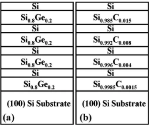
The structure of the two heterostructures used for this study is illustrated in Fig.1. The first sample is a Si/ Si1−xGex
epitaxial structure consisting of four 40 nm thick Si0.8Ge0.2
strained layers separated by 40 nm thick Si spacer layers. The second sample is a dilute Si1−yCystaircase structure
con-sisting of four Si1−yCyindividual strained layers of 30–60 nm
thickness of increasing nominal composition 共y = 0.0015, 0.004, 0.008, and 0.015 from bottom to top兲 separated by 50 nm thick Si spacers. These samples were grown by Si mo-lecular beam epitaxy 共MBE兲 in which the Si and Ge fluxes were produced by electron beam evaporation of elemental sources, while the C flux was obtained by plasma-assisted dissociation of methane in an electron cyclotron resonance 共ECR兲 source. Details on growth methodology have been reported elsewhere.11,12The average Ge concentrations in the Si1−xGex layers and C concentrations in the Si1−yCy layers
were determined by high resolution x-ray diffraction共Bruker Discover D8兲, a technique which also confirmed that both
structures were coherently stained. Details of composition depth profile were obtained by Auger electron spectroscopy 共PHI 650兲 and SIMS 共PHI Adept 1010兲 using calibration standards.具011典 cross-sectional TEM samples were prepared following standard dimpling and ion milling procedures. A 200 kV JEOL JEM-2100F TEM/STEM equipped with an ultrahigh resolution pole piece 共Cs= 0.5 mm兲, a Fischione
ADF detector共4–28 mm active diameter兲, a Gatan DigiScan, a Gatan imaging filter共GIF兲 Tridiem, and an Oxford INCA EDX was used for this study. The line scan intensity across the center of the Airy-shaped electron probe image displaces a Gaussian profile and the full width at half maximum was measured to be 0.18 nm.10With a 40 m STEM objective aperture in the JEM-2100F共this corresponds to the conven-tional TEM condenser aperture兲, the probe convergence semiangle used in this study was measured to be 14.3 mrad, which is higher than the theoretical optimal semiangle of 10.7 mrad given by 1.27共 / Cs兲1/4where is the wavelength
of the incident electrons.13 The ADF detector inner semi-angles were calibrated by recording a 具011典 zone axis Si diffraction pattern and the shadow image of the inner edge of the ADF detector simultaneously in the GIF charge coupled device camera. The ADF detector inner semiangles used were 26, 29, 38, 42, 51, 67, 78, and 92 mrad and the outer collection semiangle was the maximum value of 175 mrad accessible on the JEOL JEM-2100F with ultrahigh resolution pole piece.14 Care has been given to precisely adjust “gain” and “brightness” of the ADF detector in order to obtain ac-curate and meaningful intensity measurements.15 The thick-ness of the various TEM cross-sectional samples was deter-mined from the ratio of the plasmon to the zero-loss peaks in the electron energy loss spectrum.
III. OBSERVATIONS A. Si0.8Ge0.2sample
Figure 2共a兲 displays a low magnification ADF-STEM image of the Si0.8Ge0.2sample, and Fig. 2共b兲 is a high
mag-nification ADF-STEM lattice image from the Si1−xGex/Si
in-terface area indicated in Fig.2共a兲. The thickness of the TEM sample at the area of Fig.2共b兲is about 105 nm. As expected, Si0.8Ge0.2layers are much brighter than Si layers, consistent
with a larger average atomic number in the Si0.8Ge0.2layer
共17.6兲 than in the surrounding Si layers 共14兲. Figures 2共c兲
and 2共d兲 are high magnification ADF-STEM lattice images acquired in thicker regions of the same sample共thicknesses of 224 and 301 nm, respectively兲. With increasing sample thickness, the image resolution is preserved, but the signal to noise共S / N兲 level is reduced. This phenomenon, reported and discussed previously in other materials systems,16,17has been attributed to the increase in the effective electron probe size with increasing sample thickness leading to a loss of reso-lution and larger background.
In order to quantitatively compare the contrasts of Si0.8Ge0.2 relative to Si from low and high resolution
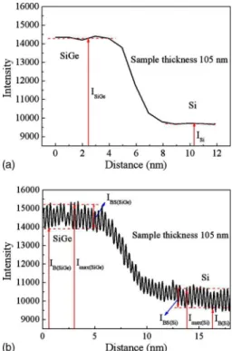
ADF-STEM images, intensity line profiles were obtained using Gatan digital micrography. Figure3 is an example of inten-sity line profiles from low and high magnification ADF-STEM images. The areas and directions of intensity line
files are indicated in Figs. 2共a兲and2共b兲. The intensity line profile was integrated over a width of 19.8 nm and along 具100典 direction for the low magnification ADF-STEM image
关Fig. 2共a兲兴, and over a width of 1.32 nm and along 具111典 direction for the high magnification ADF-STEM lattice im-age 关Fig.2共b兲兴. As shown in Fig. 3共a兲, we denote as IX the
intensity obtained from the low magnification ADF-STEM images, where X is either Si1−xGex or Si. Also indicated in
Fig.3共b兲, Imax共X兲is the mean value of the maximum intensity
of an ADF-STEM lattice image, which is measured on the 具111典 atomic columns, IB共X兲is the mean value of the intensity
of the background, which is measured between the 具111典 atomic columns. The background subtracted column inten-sity IBS共X兲is given by IBS共X兲= Imax共X兲− IB共X兲.
TableIsummarizes the various measured intensity ratios between Si1−xGex and Si 共ISiGe/ISi, Imax共SiGe兲/Imax共Si兲,
IB共SiGe兲/IB共Si兲, and IBS共SiGe兲/IBS共Si兲兲 for different TEM sample
thicknesses. The intensity ratios共and, thus, contrast between Si1−xGex and Si兲 from low resolution ADF-STEM images
共ISiGe/ISi兲 are very close to the ratios from high resolution
ADF-STEM images when the mean values of the maximum intensity measured along the 具111典 atomic columns 共Imax共SiGe兲/Imax共Si兲兲 or the mean values of the background
in-tensity measured between the 具111典 atomic columns 共IB共SiGe兲/IB共Si兲兲 are used. A closer look at the data from Table I however reveals that Imax共SiGe兲/Imax共Si兲is closer to ISiGe/ISi
than IB共SiGe兲/IB共Si兲. Thus, the intensity of low resolution
ADF-STEM images represents the mean value of the maximum intensity measured on the atomic columns of the high reso-lution ADF-STEM lattice images. In contrast the background subtracted intensity ratio共IBS共SiGe兲/IBS共Si兲兲 exhibits a peculiar
trend as a function of sample thickness. When the sample thickness is less than 100 nm, the background subtracted intensity ratio共IBS共SiGe兲/IBS共Si兲兲 is close to other intensity
ra-tios共ISiGe/ISi, Imax共SiGe兲/Imax共Si兲, and IB共SiGe兲/IB共Si兲兲, but a
sig-nificant departure is seen when the sample thickness exceeds 100 nm. As shown in Figs. 2共b兲–2共d兲, the high resolution ADF-STEM image S / N level reduces as the sample thick-ness increases. This means that Imax共x兲/IB共x兲 decreases with
increasing sample thickness. Figure4presents the plot of the absolute background subtracted intensity 共IBS共X兲兲 as a
func-tion of sample thickness for both Si1−xGex and Si. An
inter-esting observation is that with increasing thickness, IBS共SiGe兲 decreases more rapidly than IBS共Si兲. IBS共X兲represents the
con-trast between the atomic column and its background, which depends on the spatial distribution of the electron probe. This implies that any change in the probe shape traveling through the sample will affect IBS共X兲.18 The lattice of strained
FIG. 2. Low and high resolution ADF-STEM images of the Si1−xGexsample
obtained at 42 mrad ADF detector inner semiangle. The TEM sample thick-nesses are indicated in the images. Note that共b兲 is the enlargement of the square area with an arrow.
FIG. 3. 共Color online兲 Intensity line profiles of low and high resolution ADF-STEM images of Figs.2共a兲and2共b兲. IXis the intensity obtained from
the low magnification ADF-STEM images, where X is either Si1−xGexor Si.
Imax共X兲is the mean value of the maximum intensity of a high magnification ADF-STEM lattice image, which is measured on the具111典 atomic columns.
IB共X兲is the mean value of the intensity of the background, which is measured between the具111典 atomic columns. The background subtracted column in-tensity IBS共X兲is given by IBS共X兲= Imax共X兲− IB共X兲.
TABLE I. Various intensity ratios of Si1−xGexto Si measured from low and
high resolution ADF-STEM images. TEM sample
thickness
共nm兲 ISiGe/ISi Imax共SiGe兲/Imax共Si兲 IB共SiGe兲/IB共Si兲 IBS共SiGe兲/IBS共Si兲
73 1.49 1.48 1.48 1.40
105 1.45 1.44 1.44 1.37
145 1.43 1.44 1.46 1.09
224 1.43 1.43 1.45 1
301 1.40 1.40 1.42 0.82
Si1−xGex is distorted because of the misfit strain, and this
distortion is small in very thin samples due to the strain relaxation of TEM samples. But the degree of distortion in-creases with increasing sample thickness within few hun-dreds of nanometers, which likely leads to more rapid de-crease in IBS共SiGe兲 than IBS共Si兲.
The contrast共C兲 between Si1−xGexand Si defined as
C=共ISiGe/ISi兲 − 1 共1兲
varies in the range of 0.40⬍ C ⬍ 0.49 for this Si1−xGex/Si
sample 共see TableI兲. The Z contrast is expected to follow a relationship of the form C =共ZSiGe/ZSi兲n− 1 corresponding to
contrasts of 0.44 and 0.54 when n = 1.6 and 1.9, respectively.5 Because the low magnification ADF-STEM images can ac-curately reflect the contrast between Si1−xGexand Si, all
in-tensities used for the contrast calculation are from low mag-nification ADF-STEM images unless otherwise stated. An example of the intensity profile obtained from Eq. 共1兲 is shown in Fig. 5. The intensity line profile 关Fig. 5共b兲兴 was integrated over a width of 100 nm along a具100典 direction as shown in Fig.5共a兲. The intensity profile exhibits short range fluctuations in the Si1−xGexlayers and is fairly uniform in the
Si spacers. The former oscillations point to presence of varia-tions in the Ge concentration in the growth direction and will be further discussed below.
Figure6compares the evolution of contrast with sample thickness for six different ADF detector semiangles. The in-tensity of Si1−xGex共ISiGe兲 was obtained from the average of
four Si1−xGex layers 关SiGe1, SiGe2, SiGe3, and SiGe4 in
Fig. 5共a兲兴, and that of Si 共ISi兲 from the average of three Si
spacer layers关Si1, Si2, and Si3 in Fig.5共a兲兴. In all cases the following trend is observed: monotonic decrease in the con-trast with sample thickness from 50 nm to about 120 nm and almost constant contrast for samples of thickness exceeding 120 nm. The loss of contrast with increasing thickness is concomitant with a decrease in thin foil strain relaxation ef-fects as the sample thickness increases.19 It has been shown that strain relaxation in thin TEM samples is localized only near the free surface when the sample thickness is three times thicker than the strained layer thickness.20,21 With Si1−xGex layers of 40 nm thickness, the strain retained in
individual Si1−xGex layer within the TEM sample of
thick-ness exceeding ⬃120 nm will be the same. For sample thickness less than 120 nm, less misfit strain within the
Si1−xGex layers in the thinner area leads to higher contrast
between Si1−xGex and Si as compared to Si1−xGexlayers in
thicker areas. Thus, the misfit strain in the Si1−xGex layers
reduces its ADF-STEM intensity, and contributes negatively to the ADF-STEM image contrast between Si1−xGexand Si.
When the thickness is greater than 120 nm, most of the misfit strain in the Si1−xGexlayers is retained and the misfit strain
in Si1−xGex layers is the same. The contrast between the
Si1−xGexand Si is then independent of the sample thickness.
Another important observation from Fig.6 is that for a given thickness, the contrast increases with the increase in the ADF detector semiangle. The dependence of the contrast on ADF detector semiangle is further discussed in Sec. IV. B. Si1−yCy sample
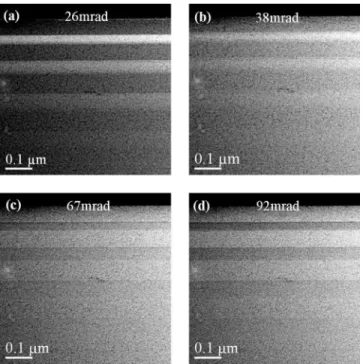
Figures 7 and 8 show two groups of 具011典 zone axis ADF-STEM images of the Si1−yCysample taken at detector
FIG. 4. 共Color online兲 Background subtracted intensity IBS共X兲 vs sample thickness for the Si1−xGex/Si heterostructure.
FIG. 5. Measurement of ADF-STEM image intensities of the Si1−xGex/Si
heterostructure.共a兲 An ADF-STEM image taken with 51 mrad ADF detector inner semiangle and sample thickness of 224 nm. 共b兲 The intensity line profile from image共a兲.
FIG. 6.共Color online兲 Variation in the contrast with TEM sample thickness at various ADF detector semiangles for the Si1−xGexon Si heterostructure.
inner-outer semiangles of 26-175, 38-175, 67-175, and 92-175 mrad. The thicknesses of the samples at the center of the image are 330 nm共Fig.7兲 and 135 nm 共Fig.8兲. For the 330 nm thick sample, it is observed that there is a large intensity difference between the Si1−yCyand Si layers at lower
detec-tor inner semiangles, which is less pronounced at larger semiangles. Contrary to the compositional contrast predic-tion of ADF-STEM imaging, the lower average atomic num-ber Si1−yCy layers are brighter than the surrounding higher
average atomic number Si for the ADF detector semiangle of up to 92 mrad共Fig.7兲. The systematic increase in intensity
from left to right in all of the images is due to increasing specimen thickness along that direction. For the 135 nm thick sample 共Fig. 8兲, this anomalous contrast between Si1−yCy and Si noted in the 330 nm thick sample is also
observed for the ADF detector semiangles of 26 and 38 mrad 关Figs. 8共a兲 and 8共b兲兴. However, the normal ADF-STEM Z contrast between Si1−yCy and Si is obtained with the ADF
detector semiangles of 67 and 92 mrad关Figs.8共c兲and8共d兲兴. The low and high magnification ADF-STEM images of the Si1−yCy sample show similar characteristics as the
Si1−xGex sample. The intensity of low magnification
ADF-STEM images represents the mean values of the maximum intensity measured on the atomic columns of the high reso-lution ADF-STEM lattice images. For the high magnification lattice images, the S / N level decreases as the sample thick-ness increases, but the image resolution is preserved 关Figs.
9共a兲–9共c兲兴. However, the background subtracted intensity
IBS共X兲of Si1−yCyon Si关Fig.9共d兲兴 shows an opposite trend to
that of the Si1−xGexon Si system in that although IBS共X兲
de-creases with increasing sample thickness as expected, IBS共SiC兲
is greater than IBS共Si兲 in all thickness regions where the
im-ages were obtained. An example of the contrast measurement for the Si1−yCysample is shown in Fig.10. Here the intensity
line profile 关Fig. 10共b兲兴 was integrated over a width of 0.48 m and along具100典 direction as shown in Fig.10共a兲.
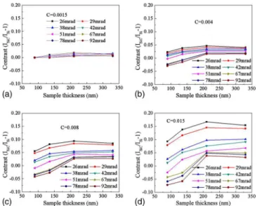
Figure 11 presents plots of the contrast dependence on sample thickness for various ADF detector semiangles for the Si1−yCy sample. The dependence of the contrast on the
sample thickness is different from that observed in the Si1−xGex sample: the contrast increases with increasing
sample thickness in the 50–200 nm range and remains almost constant in thicker samples. The contrast dependence on the ADF detector semiangle also shows an opposite trend with
FIG. 7. ADF-STEM images acquired at four different detector angles in a TEM sample of 330 nm thickness.
FIG. 8. ADF-STEM images acquired at four different detector angles in a TEM sample of 135 nm thickness.
FIG. 9. 共Color online兲 关共a兲–共c兲兴 High resolution ADF-STEM images of the Si1−yCysample obtained at 42 mrad ADF detector inner semiangle. The
thicknesses are indicated in the images.共d兲 Background subtracted intensity
IBS共X兲vs sample thickness for Si1−yCy/Si.
the contrast decreasing as the ADF detector semiangle is in-creased. To better appreciate the dependence of the contrast on the ADF detector semiangle, the data shown in Fig. 11
were replotted in Fig.12as the contrast variation as a func-tion of ADF detector semiangle at various sample thickness. For samples with thicknesses of 89 and 135 nm关Figs.12共a兲
and 12共b兲兴, the contrast between Si1−yCy and Si goes from
positive to negative as the ADF detector semiangle increases
共this is also seen in Fig.8兲. The contrast is exclusively posi-tive for samples with thicknesses of 210 and 330 nm 关Figs.
12共c兲and12共d兲兴 as seen in Fig.7. IV. DISCUSSION
The Si1−xGex/Si and Si1−yCy/Si systems exhibit opposite
ADF-STEM image contrast dependences on the ADF-STEM detector collection angles: the contrast increases with in-creasing ADF detector angle for Si1−xGex/Si共Fig.6兲, while it
decreases with increasing ADF detector angle for Si1−yCy/Si
共Figs.11and12兲. For the Si1−yCy/Si system, a unique
con-trast dependence on TEM sample thickness was observed 共Figs. 7 and 8兲. Table II summarizes some of the relevant material properties for the two samples Si0.8Ge0.2 and
Si0.985C0.015, which are used in the discussion that follows.
Here we use the highest C concentration Si0.985C0.015layer to
discuss Si1−yCy sample. The lattice constant of Si1−xGex is
obtained form the expression aSi1−xGex= aSi+ 0.0214x
+ 0.001 05x2 nm,22
while that of Si1−yCy is calculated
fol-lowing the equation aSi
1−yCy= aSi− 0.242 39y
+ 0.057 05y2 nm.23
Other physical parameters for Si1−xGex
and Si1−yCyfilms have been estimated from the data for
el-emental Si and Ge and C, using Vegard’s law, e.g., any physical parameter of an alloy is approximated by a linear interpolation of the bulk value of its constituents.
For heteroepitaxial growth of Si1−xGex or Si1−yCyfilms
on a 共100兲 Si substrate, there is a misfit strain due to the difference in lattice constants between the films and sub-strates. Since the Si substrates are much thicker than Si1−xGex or Si1−yCy layers, all the strain is assumed to be
confined to the epitaxial Si1−xGexor Si1−yCylayers. Since the
lattice constant of Si1−xGex共Si1−yCy兲 is greater 共smaller兲 than
that of Si 共Table II兲, the Si1−xGex 共Si1−yCy兲 films are under
biaxial compressive 共tensile兲 stress, resulting in the tetrago-nal distortion of the Si1−xGex共Si1−yCy兲 lattice. Here we
de-fine a coordinate system in which the y-axis is parallel to the 共100兲 growth direction and the plane containing the x- and
z-axes is parallel to the film-substrate interface plane. After
FIG. 10. Measurement of ADF-STEM image intensities of Si1−yCyand Si.
共a兲 An ADF-STEM image taken with 29 mrad ADF detector inner semiangle and sample thickness of 330 nm.共b兲 The intensity line profile from image 共a兲.
FIG. 11. 共Color online兲 Evolution of the ADF-STEM image contrast with TEM sample thickness at various ADF detector semiangles for 共a兲 Si0.9985C0.0015/Si, 共b兲 Si0.996C0.004/Si, 共c兲 Si0.992C0.008/Si, and 共d兲 Si0.985C0.015/Si.
FIG. 12. 共Color online兲 Evolution of the ADF-STEM image contrast with. ADF detector semiangles for different C concentrations at共a兲 89, 共b兲 135, 共c兲 210, and 共d兲 330 nm.
the epitaxial growth, the lattice parameters of Si remain at the bulk values of a = b = c = 0.5431 nm. For the strained Si1−xGex and Si1−yCy films, the in-plane lattice parameters
are constrained to match the substrates values, a = c = 0.5431 nm, so the strain displacement along x and z direc-tions is 0.5474– 0.5431= 0.0043 nm for Si1−xGex and
0.5395– 0.5431= −0.0036 nm for Si1−yCy. From linear
elas-ticity theory, the perpendicular lattice constant of the film, b, is given by 兵1 − 关2/共1 −兲兴f其a and has a greater value b = 0.5511 nm for Si1−xGex and a smaller value b
= 0.5367 nm for Si1−yCy film. For defect-free crystals, the
ADF-STEM image intensity can be fully accounted for by elastic scattering and thermal diffuse scattering共TDS兲.24The differential cross sections for elastic scattering and TDS are given by25,26
冋
d共兲 d⍀册
Elastic =4␥ 2Z2 a0 2 k0 4 1 共2+ 0 2兲2兵exp关− 2共M T兲2兴其, 共2兲冋
d共兲 d⍀册
TDS =4␥ 2Z2 a02k04 1 共2 +02兲2兵1 − exp关− 2共M T兲2兴其, 共3兲 where0=共k0r0兲−1 is the characteristic angle of elasticscat-tering, k0= 2505 nm−1 is the wave vector 共at 200 keV兲, r0
= a0Z−1/3 is a screening radius, a0= 0.0529 nm is the first
Bohr radius, ␥= 1.394 共at 200 keV兲 is a relativistic factor, and Z is the average atomic number. MT= 82u
T
2/
2
is the Debye–Waller factor and uTis the amplitude of thermal
vi-bration.
The scattering of the incident electrons from a random strain field can be treated similarly to that from TDS, and an extra Debye–Waller factor can be added to the cross section of TDS to account for the strain effect:10
冋
d共兲 d⍀册
TDS+Strain =4␥ 2Z2 a02k04 1 共2 +02兲2兵1 − exp关− 2共M T + MS兲2兴其, 共4兲 where MS= 82u S 2/ 2and uS is the amplitude of the strain.
Figure13shows plots of关d共兲 / d⍀兴 as a function of
for Si, Si1−xGex, and Si1−yCy using Eqs. 共2兲–共4兲. Insets of
Figs.13共a兲and13共b兲are rescaled plots for showing the cross section differences between Si and Si1−xGex, and between Si
and Si1−yCyat high scattering angle . At high, TDS 共for
Si兲 or TDS plus strain 共for Si1−xGexand Si1−yCy兲 dominates
the ADF-STEM image intensity. For the Si1−xGexsample, the
cross section of Si1−xGex is always greater than that of Si
mainly due to the higher Si1−xGex atomic number. In other
words, composition plays a crucial role in ADF-STEM im-age contrast for the Si1−xGexsample. In the Si1−yCysample,
TABLE II. Properties of Si0.8Ge0.2and Si0.985C0.015.
Si Ge C Si0.8Ge0.2 Si0.985C0.015
Lattice constant a共nm兲 共before epitaxy兲 0.5431 0.5658 3.567 0.5474 0.5395
Misfit strain displacement共nm兲 0 ⫺0.0043 0.0036
Lattice misfit f共%兲 0 ⫺0.83 0.66
Average atomic number 14 32 6 17.6 13.88
Poisson’s ratio 0.28 0.26 0.10 0.28 0.28
Elemental radius共nm兲 0.120 0.117 0.068 Amplitude of thermal vibration at room temperature uT
共nm兲 0.0078 0.009 0.005 0.008 0.0078
FIG. 13. 共Color online兲 Variation in the scattering cross section with the scattering angle of elastic scattering, TDS, and TDS with strain for 共a兲 Si0.8Ge0.2/Si and 共b兲 Si0.985C0.015/Si. Panel 共c兲 shows the dependence of contrast on scattering angle calculated from共a兲 and 共b兲 for Si0.8Ge0.2/Si and Si0.985C0.015/Si.
the average atomic number for the highest C concentration layer Si0.985C0.015is 13.88共see TableII兲, and very close to 14
of Si. In this case, the angular distribution term关the term in the square parentheses in Eqs.共3兲and共4兲兴 plays a very sig-nificant role in the ADF-STEM image intensity. It is ob-served from the inset of Fig.13共b兲 that the cross section of Si1−yCyis greater than that of Si only when⬍ 48.1 mrad.
To understand the observed opposite dependences of the contrast on the ADF detector angle for the Si1−xGex/Si and
Si1−yCy/Si systems, the intensity collected by the ADF
de-tector was calculated by integrating the cross section over the detector geometry. Note that the total intensity of an ADF-STEM image arises from both elastic, TDS and strain 共if any兲, and therefore the cross section of elastic scattering should be included in the calculation共its contribution is par-ticularly important in the low ADF detector angle range兲. Figure13共c兲shows general agreement of the contrast depen-dence on ADF detector angle with experimental observa-tions: for Si1−xGex/Si, the contrast increases with increasing
ADF detector angle, while the contrast decreases with the increase in ADF detector angle for Si1−yCy/Si. The simple
atomic scattering model explains the general trends observed in the ADF-STEM imaging contrast for epitaxial strained Si1−xGex and Si1−yCy on 共001兲 Si. However, it should be
noted that the differential cross section applies to a single atom, and neglects some experimental factors that contribute to the ADF-STEM image intensity such as sample thickness, beam convergence angle, probe size, and multiple electron scattering effects. Nevertheless, the single atomic scattering is the basis of accurate multislice calculation, and this simple approach agrees with the observed dependence of ADF-STEM image contrast on detector semiangle for both Si1−xGex/Si and Si1−yCy/Si systems.
To understand the different ADF-STEM image contrast dependences on sample thickness in the Si1−yCy sample
共Figs.7 and 8兲, multislice calculations were performed fol-lowing earlier work on the dilute GaNAs/GaAs system.10 In multislice calculations, the sample thin foil is divided into a series of thin lamellas and the electron beam is propagated sequentially through each layer. The ADF-STEM image in-tensity is obtained by integrating the inin-tensity of the conver-gent beam electron diffraction pattern over the range of inner and outer semiangles of the detector for each pixel in the image. For the GaNAs/GaAs system, the displacement around substitutional N atoms was found to play a critical role in determining the ADF-STEM contrast between dilute GaNAs and GaAs. Likewise, the lattice misfit strain in the dilute Si1−yCy/Si system gives the average effects of strain
over a large volume. On an atomic scale however, there are local variations in the strain arising from radial displace-ments around substitutional C atoms in the Si1−yCy lattice
because the C atomic radius of 0.068 nm is much smaller than the 0.120 nm atomic radius of the Si host atoms. For Si1−xGexlattice, this local variation in the strain is very small
because of the similar atomic radii of Ge共0.117 nm兲 and Si. The displacement共u兲 of the atoms surrounding each substi-tutional Si atom in Si1−yCy due to the atomic radius
differ-ence between Si and C atoms can be modeled using linear elasticity theory in the isotropic approximation as
u=共c/r3兲r, 共5兲
where c is a constant dependent on the degree of lattice distortion around the C atoms and r is a position vector in the lattice. A value for c can be estimated from elasticity theory,27 da a = 4 1 − 1 + yc ⍀, 共6兲
where y is the C concentration,= 0.28 is Poisson’s ratio for Si, da / a is a measure of the lattice misfit with da = aSi
− aSi1−yCy= 0.0036 nm, and ⍀ = 20.02⫻ 10−3 nm3 is the
vol-ume per atom in the lattice. Substituting these values into Eq.
共6兲 gives c = 1.25⫻ 10−3 nm3. The magnitude of the atomic
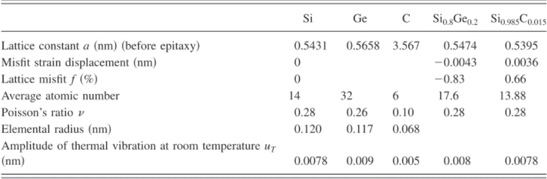
displacements predicted using Eqs.共5兲 and共6兲 is plotted in Fig.14and it is observed that for the first and second nearest neighbor atoms 共0.2352 and 0.3843 nm, respectively兲 the displacements are significantly greater than those arising from uniform lattice misfit strain. Also included in Fig.14is comparison of uniform misfit strain and local displacement around Si for Si1−xGex. The displacement is negligible for
Si1−xGexas expected.
In the multislice simulation, carbon was incorporated into the Si0.985C0.015layer by first randomly substituting 1.5%
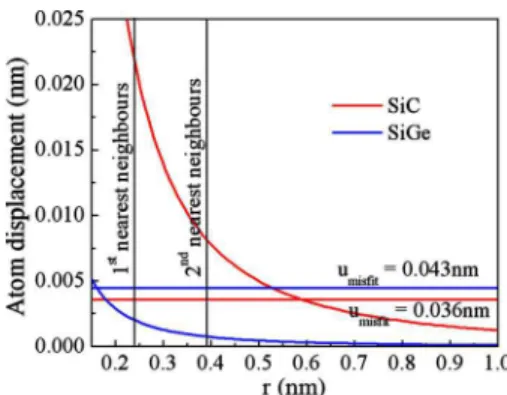
of the Si atoms with C atoms and then displacing the atoms in the lattice to account for the strain around the C atoms. Figure 15compares multislice simulation results for Si and Si1−yCyintensity in ADF-STEM images for various
scatter-ing anglesfor two different sample thicknesses of共a兲 134.4 and 共b兲 326.4 nm. For 134.4 nm thick sample, the strained Si1−yCy scatters more intensity than Si for ⬍⬃ 50 mrad,
and scatters less intensity than Si for⬎⬃ 50 mrad, which is in agreement with the experimental observations in the 135 nm thick sample as shown in Fig. 8: the Si1−yCy is
brighter than Si when ADF detector semiangles are 26 and 38 mrad, but darker than Si when ADF detector semiangles are 67 and 92 mrad. For the 326.4 nm thickness sample, the multislice simulation predicts that Si1−yCy should scatter
more intensity than Si for all values, which again agrees with the experimental observations in the 330 nm thick sample as shown in Fig. 7: the Si1−yCy is brighter than Si
when ADF detector semiangles are 26, 38, 67, and 92 mrad. Finally, like the contrast dependence on the ADF detec-tor collection angle, the Si1−xGex/Si and Si1−yCy/Si systems
FIG. 14. 共Color online兲 Comparison of the displacement around a substitu-tional C and Ge atom with lattice misfit displacement in Si0.985C0.015and Si0.8Ge0.2.
also exhibit opposite ADF-STEM image contrast depen-dences on TEM sample thickness in relatively thin sample areas: the contrast decreases with increasing thickness for sample thickness less than ⬃120 nm for Si1−xGex system
共Fig. 6兲, while the contrast increases with increasing thick-ness for sample thickthick-ness less than⬃200 nm for Si1−yCy/Si
system 共Fig. 11兲. In the relatively thick sample areas, the contrast is independent of sample thickness for both Si1−xGex/Si and Si1−yCy/Si systems. The contrast
depen-dence on the TEM sample thickness is likely related to the facts that composition plays a crucial role in ADF-STEM image contrast for the Si1−xGex/Si system, and strain
dis-placement around substitutional C atoms play a critical role in determining the ADF-STEM contrast in Si1−yCy/Si
sys-tem. Further theoretical works need to be done to fully un-derstand the contrast dependence on TEM sample thickness for heteroepitaxial films.
V. APPLICATIONS
ADF-STEM imaging combined with EDX and EELS al-lows the simultaneous characterization of crystal morphol-ogy, structure, and composition in a STEM. Here both EDX and EELS could determine the Si and Ge compositions in the Si0.8Ge0.2 sample, but failed to determine C in the Si1−yCy
sample because of a C concentration below detection limit. Figure16compares Ge compositions obtained by EDX and EELS to the ADF-STEM image line profile of Fig. 5共b兲. In order to ease comparison of the composition profiles, the EDX and EELS Ge composition curves were moved up by 10% and 20%, respectively, while the ADF-STEM intensity line profile was adjusted so that average Si intensity coin-cides with zero, and the average Si1−xGexintensity was set to
20%. The similarity of the Ge composition profiles measured
by the EDX or EELS and the ADF-STEM image contrast profile is striking. The local variations in the ADF-STEM contrast is clearly correlated with fluctuations in the Ge con-tent within the films detected with the other analytical tech-niques and arising from Ge atomic flux instabilities during deposition. Furthermore, the magnitude of the ADF-STEM contrast variations scales precisely with the Ge content varia-tions as determined by the analytical techniques. This shows that for this materials system, ADF-STEM image contrast analysis can be an accurate alternative method for evaluating material composition fluctuations in thin alloy heterostruc-tures.
In the Si1−yCy/Si system, despite the fact that the C
con-centration was beyond the detection limit of both EDS and EELS, a strong contrast between Si and Si1−yCy layers was
observed in certain ADF-STEM images. 共See, for example, an ADF-STEM image acquired at 29 mrad detector semi-angle and 330 nm sample thickness关Fig.10共b兲兴.兲 To verify whether or not this contrast can be correlated with the C composition of the layers, the C composition profile of the Si1−yCysample was obtained by SIMS. Figure17is the
com-parison of C composition as obtained by SIMS with the ADF-STEM image line intensity profile shown in Fig.10共b兲. By adjusting the Si0.985C0.015layer ADF-STEM image
inten-sity to a 1.5 at. % C peak concentration, the C composition profiles as determined by SIMS coincide remarkably well with the ADF-STEM image line intensity profile for all four Si1−yCy layers. In conjunction with another analytical
tech-nique such as SIMS or x-ray diffraction, the ADF-STEM image line intensity profile of dilute Si1−yCy/Si system may
FIG. 15. 共Color online兲 Multislice calculation of the intensity for Si and Si1−yCylayers for TEM sample thicknesses of共a兲 134.4 and 共b兲 326.4 nm.
FIG. 16. 共Color online兲 Comparison of Ge composition profiles obtained from EDX and EELS with the ADF-STEM image intensity line profile.
FIG. 17. 共Color online兲 Comparison of the C composition profile as ob-tained from SIMS with the ADF-STEM image intensity line profile.
thus provide a means to estimate C concentration variation in the Si1−yCy/Si system at concentrations beyond the detection
limit of either EDX-STEM or EELS-STEM. In fact, details of the STEM-ADF C concentration profile in Fig.17may be linked to experimental conditions prevailing during the MBE deposition of the Si/ Si1−yCystaircase structure. For example,
the slow increase in C content from the bottom to top in the more dilute layers may be correlated with transients and sta-bilization periods of the ECR plasma C source. Instabilities in the ECR source may also have caused local C composition variations that are revealed by spikes in the ADF-STEM pro-file, but that could not be resolved by SIMS. Also, ADF-STEM exhibits a better depth resolution than SIMS and re-veals that the Si/ Si1−yCy interfaces chemically sharper than
what SIMS would suggest. Finally, it is interesting to note that the integrated ADF-STEM intensity from the upper Si1−yCy layers is somewhat lower than that observed in
SIMS. This may be correlated with the fact that some C atoms are known to occupy nonsubstitutional sites in epitax-ial Si1−yCylayers with C composition in excess of 0.01. This
may indicate that here the nonsubstitutional C fraction does not contribute significantly to the ADF-STEM contrast. VI. CONCLUSION
In this study we have shown that experimental factors such as TEM sample thickness, ADF detector inner angle, and strain at the atomic scale can influence the ADF-STEM image contrast between heteroepitaxial layers and substrates. For strained Si1−xGex layers on Si the ADF-STEM image
contrast decreases with increasing thickness, and remains al-most constant after the sample thickness exceeds 120 nm. The contrast was also found to increase with the increase in the ADF detector semiangle. In the Si1−yCy/Si system,
con-trast shows an opposite thickness and ADF detector semi-angle dependence of the ADF-STEM image contrast: the contrast increases with increasing sample thickness and de-creases with increasing ADF detector semiangle, but the con-trast remains almost constant after the sample thickness ex-ceeds 200 nm. The dilute Si1−yCy/Si system also showed
some unique contrast characteristics: contradictory to the compositional contrast prediction of ADF-STEM image in-tensity, the lower average atomic number strained Si1−yCy
layers were always brighter than the higher average atomic number Si when the sample thickness is greater than 200 nm. In thinner samples, this anomalous contrast was observed for an ADF detector semiangle of up to 50 mrad. Atomic scat-tering calculations correctly predict the ADF-STEM image contrast dependence on the ADF detector semiangles for
both Si1−xGex/Si and Si1−yCy/Si systems. Multislice
simula-tions show that the anomalous ADF-STEM image contrast in Si1−yCy/Si system can be explained by local strain effects in
proximity of small radius substitutional atoms. For both ma-terials systems, the intensity line profile of the ADF-STEM images showed excellent agreement with composition pro-files obtained with analytical TEM techniques: EDX and EELS, as well as SIMS. In this context, ADF-STEM can be seen as an alternative method to quickly estimate concentra-tion and composiconcentra-tion fluctuaconcentra-tions in thin layered media. ACKNOWLEDGMENTS
The authors thank G. Parent for TEM sample prepara-tion, S. Rolfe for the SIMS measurements, I. Sproule for the Auger measurements, and M. Robertson for providing the original multislice calculation codes.
1
E. P. O’Reilly,Semicond. Sci. Technol.4, 121共1989兲. 2
P. M. Mooney and J. O. Chu,Annu. Rev. Mater. Sci.30, 335共2000兲. 3
D. B. Williams and C. B. Carter, Transmission Electron Microscopy 共Ple-num, New York, 1996兲, p. 360.
4
D. E. Jesson, S. J. Pennycook, and J.-M. Baribeau,Phys. Rev. Lett.66,
750共1991兲. 5
P. Hartel,Ultramicroscopy63, 93共1996兲. 6
S. J. Pennycook and D. E. Jesson,Phys. Rev. Lett.64, 938共1990兲. 7
P. Rez and D. A. Muller,Annu. Rev. Mater. Res.38, 535共2008兲. 8
D. D. Perovic, C. J. Rossouw, and A. Howie,Ultramicroscopy 52, 353
共1993兲. 9
Z. Yu, D. A. Muller, and J. Silcox,J. Appl. Phys.95, 3362共2004兲. 10
X. Wu, M. D. Robertson, J. A. Gupta, and J.-M. Baribeau,J. Phys.: Con-dens. Matter20, 075215共2008兲.
11
J.-M. Baribeau, D. J. Lockwood, M. W. C. Dharma-Wardana, N. L. Row-ell, and J. P. McCaffrey,Thin Solid Films183, 17共1989兲.
12
J.-M. Baribeau, D. J. Lockwood, J. Balle, S. J. Rolfe, G. I. Sproule, and S. Moisa,Thin Solid Films410, 61共2002兲.
13
J. C. H. Spence, High Resolution Electron Microscopy, 3rd ed.共Oxford University Press, New York, 2003兲, p. 253.
14
M. Kawasaki, personal communication共July 2006兲. 15
X. Wu, M. D. Robertson, J. A. Gupta, J.-M. Baribeau, J. C. Bennett, M. Kawasaki, and T. Aoki, Mater. Res. Soc. Symp. Proc. 982E, KK01-03 共2007兲.
16
A. C. Diebold, B. Foran, C. Kisielowski, D. A. Muller, S. J. Pennycook, E. Principe, and S. Stemmer, Microsc. Microanal. 9, 492共2003兲.
17
D. O. Klenov and S. Stemmer,Ultramicroscopy106, 889共2006兲. 18
J. Liu and J. M. Cowley,Ultramicroscopy52, 335共1993兲. 19
J. M. Gibson, R. Hull, J. C. Bean, and M. M. J. Treacy,Appl. Phys. Lett.
46, 649共1985兲. 20
M. M. J. Treacy and J. M. Gibson,J. Vac. Sci. Technol. B4, 1458共1986兲. 21
D. D. Perovic and G. C. Weatherly, Philos. Mag. A 64, 1共1991兲. 22
J. P. Dismukes, L. Ekstrom, and R. J. Paff, J. Phys. Chem. 68, 3021
共1964兲. 23
P. C. Kelires,Phys. Rev. B55, 8784共1997兲. 24
L. Wang and J. M. Cowley,Ultramicroscopy31, 437共1989兲. 25
R. F. Egerton, Electron Energy-Loss Spectroscopy in the Electron
Micro-scope, 2nd ed.共Plenum, New York, 1996兲, p. 134. 26
C. R. Hall and P. B. Hirsch, Proc. R. Soc. London, Ser. A 286, 158共1965兲. 27