Publisher’s version / Version de l'éditeur:
Vous avez des questions? Nous pouvons vous aider. Pour communiquer directement avec un auteur, consultez la première page de la revue dans laquelle son article a été publié afin de trouver ses coordonnées. Si vous n’arrivez Questions? Contact the NRC Publications Archive team at
[email protected]. If you wish to email the authors directly, please see the first page of the publication for their contact information.
https://publications-cnrc.canada.ca/fra/droits
L’accès à ce site Web et l’utilisation de son contenu sont assujettis aux conditions présentées dans le site LISEZ CES CONDITIONS ATTENTIVEMENT AVANT D’UTILISER CE SITE WEB.
Student Report; no. SR-2009-02, 2009-01-01
READ THESE TERMS AND CONDITIONS CAREFULLY BEFORE USING THIS WEBSITE.
https://nrc-publications.canada.ca/eng/copyright
NRC Publications Archive Record / Notice des Archives des publications du CNRC : https://nrc-publications.canada.ca/eng/view/object/?id=012d6f8a-182e-4f09-aa91-1d2257c9af0a https://publications-cnrc.canada.ca/fra/voir/objet/?id=012d6f8a-182e-4f09-aa91-1d2257c9af0a
NRC Publications Archive
Archives des publications du CNRC
For the publisher’s version, please access the DOI link below./ Pour consulter la version de l’éditeur, utilisez le lien DOI ci-dessous.
https://doi.org/10.4224/18227303
Access and use of this website and the material on it are subject to the Terms and Conditions set forth at Development of a Digitally Programmable Signal Conditioner.
National Research Council Canada Institute for Ocean Technology Conseil national de recherches Canada Institut des technologies oc ´eaniques
SR-2009-02
Student Report
Development of a Digitally Programmable Signal
Conditioner
Zhao, F.
DOCUMENTATION PAGE
REPORT NUMBER SR-2009-02
NRC REPORT NUMBER DATE
April 24, 2009 REPORT SECURITY CLASSIFICATION
Unclassified
DISTRIBUTION Unlimited TITLE
Development of Digitally Programmable Signal Conditioner
AUTHOR(S) Feng Zhao
CORPORATE AUTHOR(S)/PERFORMING AGENCY(S)
National Research Council, Institute for Ocean Technology PUBLICATION
N/A
SPONSORING AGENCY(S)
IMD PROJECT NUMBER NRC FILE NUMBER
KEY WORDS
Signal conditioner, Testing, Signal conditioning, Design
PAGES iii, 15, Apps. 8 FIGS. 13 TABLES 2 SUMMARY
This report shows the continuing design and testing of a new digitally programmable signal conditioner for general-purpose use at IOT. Includes prototype test, analog input control, offset adjustment and digital filter design.
ADDRESS National Research Council Institute for Ocean Technology Arctic Avenue, P. O. Box 12093 St. John's, NL A1B 3T5
National Research Council Conseil national de recherches Canada Canada Institute for Ocean Institut des technologies
Technology océaniques
DEVELOPMENT OF DIGITALLY PROGRAMMABLE SIGNAL
CONDITIONER PROTOTYPE
SR-2009-02
Feng Zhao
ACKNOWLEDGEMENTS
The author would like to thank David Millan for his sponsorship, supervision, and mentoring throughout the term. Acknowledgements also go to Pete Hackett. Thanks also to everyone at IOT.
SUMMARY
This report covers the continuation of work started by Kevin Murrant on a digitally programmable signal conditioner. The signal conditioner is being developed as a replacement for older general-purpose models currently in use at IOT. An initial prototype identifying the basic parts of the system, and a single channel
prototype were developed last term. In this report, that single channel prototype is assembled and tested. The report also shows analog input control, offset adjustment and digital filter design.
TABLE OF CONTENTS
1.0 INTRODUCTION ... 1
1.1 Existing Signal Conditioning... 1
1.2 Digitally Programmable Signal Conditioner ... 2
2.0 PROTOTYPE... 3 3.0 TESTING ... 5 3.1 Hardware Test... 5 3.2 Software Test ... 5 4.0 DESIGN... 7 4.1 Power Supply ... 7 4.2 Software ... 8 4.3 Relay Control ... 8 4.4 Offset Adjustment... 9 4.5 Digital Filter ... 10 5.0 Results... 12 6.0 Continuation... 15 LIST OF FIGURES Figure 1. Schematic... 3
Figure 2. Image of Completed Board……….4
Figure 3. Menu Layout………..5
Figure 4. QF1D512-DK Digital Filter Development kit……….…6
Figure 5. Power Supply Circuit Diagram………7
Figure 6. Power Supply Layout………...7
Figure 7. Autozero Circuit………...……….9
Figure 8. Software Controllable Offset……….10
Figure 9. Functional Block Diagram of Digital Filter Section………11
Figure 10. Flow Chart of Operation Menu for Single Channel Prototype…….12
Figure 11. FFT and Time-domain output data………..13
Figure 12. FFT and Time-domain output data………..13
Figure 13. FFT and Time-domain output data………..14
LIST OF TABLES Table 1. Relay Truth Table……….8
Table 2. Relay Setting for Signal Switching……….9 APPENDICES
DEVELOPMENT OF DIGITALLY PROGRAMMABLE SIGNAL CONDITIONER
1.0 INTRODUCTION
Within the Institute for Ocean Technology (IOT) exists several facilities for
conducting scale model tests under various ocean environments and conditions. These facilities include an ice tank, cold room, offshore engineering basin,
cavitation tunnel, and towing tank. Generally, a scale model is constructed of the design under study, the model is placed in the environment of interest, and data is recorded.
Test data is acquired via various transducers that convert the physical property of interest into an electric signal. Common transducers include pressure sensors, temperature sensors, strain gauges, wind gauges, wave height probes, etc. In practice, many transducers may be used in a single experiment in order to gather all required data.
The signal produced by a transducer is usually quite small and is subject to interference from a variety of environmental sources. These sources include radio frequency (RF) interference, electromagnetic interference, and electrostatic discharge. This interference is obviously unwanted and steps are taken to reduce the effects of these sources on the signal of interest.
Signal conditioning is used to amplify the signal, filter out interference, and produce an output that is suitable for measurement or digitization. This
conditioning is performed in stages and varies based on the type of signal being used. Precision and accuracy are integral in the model testing performed at IOT. Therefore, the signal conditioning must be very precise and allow as little
interference as possible.
1.1 Existing Signal Conditioning
Several signal conditioning systems are currently in use at IOT. Many of these are specific implementations that are required depending on the project.
However, a general purpose signal conditioner exists that is used in most data acquisition situations.
The existing general purpose signal conditioner is based around a single chip that provides most of the necessary components. This chip is the Analog Devices 1B31 strain gauge signal conditioner. Configuration of the chip is accomplished via external jumpers, resistor values, and capacitor values. A single chip is required for each channel of signal conditioning. 16 channels exist in the current system.
Configuration requires external components, and a technician must manually set up each channel for each test. This method is susceptible to configuration error, either by placing a component with an incorrect value or by varying tolerances within components. Therefore, repetition of a specific test configuration is not always possible.
However, despite drawbacks, the current signal conditioner fulfills the
requirements for most general purpose signal conditioning needs at IOT. The current problem is that the units are breaking down with use, and the 1B31 chip they are based on has been discontinued. This makes repair of the units
expensive and difficult.
1.2 Digitally Programmable Signal Conditioner
The existing signal conditioner will be replaced by a new design and will have digital programmability as a requirement; however, why we still need a new digitally programmable signal conditioner since several signal-conditioning systems are currently used at IOT?
The new design is intended to be more modular, allowing replacement of
components as new technology becomes available, or if an existing component is discontinued. This will prevent the repair problem of the previous system and allow the new unit to serve for a longer period of time.
The new system should at least serve the same functionality of the existing unit. The addition of digital programmability will eliminate the need for manual
configuration, reducing set up time and improving repeatability. The new design will also address certain mechanical limitations of the previous system. The transducer cable connectors were previously soldered directly to the circuit board, placing strain on the solder connections and the board when
connecting/disconnecting cables. The new connectors should have some strain relief to prevent this from happening.
2.0 PROTOTYPE
A full schematic was created for the single-channel prototype including all of the features mentioned in the previous section. Once this schematic was completed, the parts required for assembly were ordered for proceeding to a PCB layout. The parts were required to assist in the selection of footprints for each
component. Below is the full schematic.
Figure 1. Schematic
The prototype board is designed for a single channel test. Once the board was completely assembled, the software could be downloaded to the CUBLOC
processor by the RS-232 connector, so that the codes for the processor could be updated and the function of the board could be tested and troubleshot. An image of the completed board is shown below.
Figure 2. Image of completed board
A LCD and keypad are supplied by COMFILE as part of their system, and the processor has built in interfaces to communicate with these devices. The LCD screen shows all the operation menus for the prototype. By using the input keypad, users can select different functions of the prototype. This report will show how the operation menus work after the development and testing was finished.
3.0 TESTING
Once the software was downloaded to the CB220, the first troubleshooting
processes could take place. Some of the problems encountered are documented below.
3.1 Hardware Test
The power supply for the prototype has not been designed. So far the prototype uses four wires connected between to two voltage generators and the power junctions on the prototype board. Initially, the board was drawing too much current and the power supply was being current limited. This was eventually found to be due to the +/- 5V regulators being used on the board. These were removed and replaced with higher current devices which were attached by soldering wires to the board and gluing the regulators to the back of the board. 5 out of 8 relays were working correctly except relays 1, 2, and 3. Functions for those three relays would be tested. At the beginning of the test, the interface was working for the majority of the features, except parts of the relay control, offset adjustment, and digital filtering.
3.2 Software Test
The code for the interface and control was written in BASIC programmed with the COMFILE CUBLOC studio. The software uses a user interface menu organized in the following way.
Main menu Gain AD624 1
Filter Set Vargain Set
Figure 3. Menu layout Offset Bode Verify ATT. 100 On 200 Set Off 500 Diff. inputs Single ended DC input Freq. response
Some compiling issues were noticed for the codes for CB220 at the beginning. Some of the functions haven’t been coded yet, such as analog inputs control, calibration. So that would cause the LCD to not display all the option menus, therefore some functions could not be tested at that time.
A communication error occurred when downloading the code to the CB220. That could be the problem of the RS-232 connector or the chip itself had been
damaged during previous use. By removing the CB220 onto another study board, the code was successfully downloaded to the chip, which means the cable for the RS-232 connector might have been broken.
Since it is not possible to determine whether the subroutine for downloading coefficients to the filter is working correctly, further tests for the prototype would simply by pass the filter section using the pin headers on the board. The
QUICKFILTER QF1D512-DK development kit was used for testing and filter design instead of the digital filter that was the by-pass on the prototype board.
4.0 DESIGN
When all the problems occurred when testing the prototype were fixed, the design process to complete all functions for the prototype could take place.
4.1 Power Supply
The power supply must be designed to provide a variety of bi-polar voltages to the variety of components to use, such as the microcontroller, which requires +/- 12V and +/-5V DC. The power supply must introduce as little noise as possible to the system, and effort must be exerted in keeping separate the signal from the power supply interface. The power supply was designed to support +/-15V and +/-5V DC inputs for the prototype, and the circuit diagram and layout are shown below.
Figure 5 Power supply circuit diagram
4.2 Software
Subroutines have been written to interface to the various IC’s. These subroutines provide an easy to use way of sending serial data in the correct format to each component. For example, to switch the relay on port 1 to on, the command would be:
RelaySet 1,1
Subroutines such as this have been written for each programmable device. See Appendix A for a code listing.
4.3 Relay Control
There are 8 relays used in the prototype board for signal switching and gain setting. The test before shows that the relay control for input signal switching has not finished yet. This section will show how to control the relays by using the microprocessor.
The previous tests have shown 3 relays related to the input signal control, and the number of these relays could be found by schematic, which are number 1, 2, and 3. The table below shows the list of three relays with their different states.
Relay Relay state
LS1 ON ON ON ON OFF OFF OFF OFF
LS2 ON ON OFF OFF ON ON OFF OFF
LS3 ON OFF ON OFF ON OFF ON OFF
Table 1. Relay truth table.
With this table above, a test could be made for testing 8 different relay statuses. When relay 2 stays ON, no matter what the other two relays switch ON or OFF, both of the input signals will be sent into the AD624. However, when relay 2 switches OFF, and relay 3 switches ON, one of the input signals will be grounded. That will separate differential and single ended statuses for the instrumentation amplifier AD624. A +15VDC input passing through a voltage divider is controlled by relay 1. If relay 1 stays ON and relays 2 and 3 stays OFF, the 10 m VDC steady output will be sent into the analog devices. The sine wave generator is an analog devices AD9833 signal generator IC capable of frequency sweep, which would be used to verify the frequency response of the system. Since all of the relays 1, 2, and 3 switch OFF, this analog device would communicate with the AD624 and start to verify the frequency response. The table below summarizes all the results of the analog input control tests.
LS2: ON Differential inputs LS2: OFF LS3: ON Single Ended LS1: ON LS2 & LS3: OFF DC input
LS1, LS2, & LS3: OFF Frequency response
Table 2. Relay setting for signal switching. 4.4 Offset Adjustment
The initial design of the programmable signal used a hardware solution for offset adjustment. The Autozero Circuit for the hardware solution shows below.
Figure 7. Autozero Circuit
After integrating all components into the final prototype, the hardware solution for offset adjustment was no longer used. To provide very accurate data in high gain configurations, a software solution would support programmable controllability for offset adjustment. A CMOS DAC operating in the bipolar mode and connected to the reference terminal provides software controllable offset adjustments.
Figure 8. Software Controllable Offset
In the prototype schematic of the single channel signal conditioner, an analog device AD711AQ low noise op-amp is used for the D/A to operate in bipolar mode. Then, Analog Devices AD44X series are used for D/A reference. The AD5542 defines the output, which is using 16-bit serial interface.
Subroutine for offset adjustment has been written. See Appendix A for offset adjustment code.
4.5 Digital Filter
The frequencies that normally IOT is dealing with are less than 1KHz; therefore, the filter should be designed as low pass filter with varying cut off frequencies. A Clock Oscillator provides a clock signal with 100KHz to the Bipolar
Programmable Input ADC (analog-to-digital converter), Analog Device Bipolar Voltage Output AD5542, and the digital filter. The analog filters, such as the Anti-Aliasing filter has a fixed signal bandwidth of 25KHz. The block diagram of this section is shown below.
Figure 9. Functional block diagram of digital filter section The digital filter was designed by using the QFPRO filter design software. As mentioned in previous sections, the QUICKFILTER QF1D512-DK development kit in use for designing and testing the digital filter section instead of the digital filter built in the prototype board, which has been by-passed. All the filters designed for testing the prototype was low-pass windowed SINC Blackman-Harris 7-term, with orders of 8. With such a low order of 8, the designed low-pass filter would not perform a very sharp drop, however, that could avoid phase shifting problems during the test. Some filters were designed for testing the results with cut of frequencies of 100Hz, 50Hz, 10Hz, and 1Hz with orders of 8, and the results of them will be shown in the results section. Later, a low-pass filter with 512 orders, and a cut-off frequency of 110Hz was designed as well.
Digital Filter QF1D512 16-BIT D/A A/D 16-BIT COMFILE PLC
Sampling in Sampling out
5.0 RESULTS
After downloading the complete software into the processor, the interface and board control could be navigated by pressing a key of the input keypad, which corresponding to a number next to each option menu. Currently, all features shown below are working fine, except the Bode section.
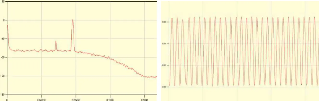
The best method to show the digital filter performance is FFT (Fast Fourier Transform) and Time-Domain data. The digital filter results are available through the QFPRO filter design software. However, the data can be transferred in raw format to a file for saving, and the data also can be processed by another software. The filter coefficients of the low pass filter designed with 512 orders have been successfully downloaded into the microcontroller CB220. Below shows three filters testing results, as previously discussed, however, the result for 1Hz filter is not included. To test the 1Hz filter, an input signal was sent in with frequency of 0.5 Hz, amplitude of 10mV, and a gain of 100. The test was failed to separate the spectrum in FFT and capture the output signal in Time-Domain. All the data was tested in single channel.
Figure 11. FFT and Time-domain output for 100Hz filter.
Input is 80Hz sine wave, amplitude of 10mV, with gain of 1.
Figure 12. FFT and Time-domain output for 50Hz filter.
Input is 40Hz sine wave, amplitude of 10mV, with gain of 100
Figure 13. FFT and Time-domain output for 10Hz filter.
6.0 CONTINUATION
Power supply should be added to the prototype, and that will make further application of the prototype more convenient. The digital filter section is not yet completed. Filter coefficients have been successfully downloaded to the
processor, however, how to communicate between the microcontroller and the filter is still an unsolved problem. With the filter coefficients the processor should have a method to control the digital filter to perform as a varying cut-off
frequencies low pass filter.
The function Bode is prepared for bode plot, and this part of work has not started yet. One general idea for this function is that the CUBLOC Studio might have a way to check the output; and another D/A could be added to sample the output; or find out where the digital output could be read before it reached the final D/A. Multi-channel signal conditioning system could be started since all problem left so far would be done.
References
[1] Analog Devices, Inc., "AD624 Precision Instrumentation Amplifier," Analog Devices, Inc., 1999. [Online]. Available:
http://www.analog.com/UploadedFiles/Data_Sheets/AD624.pdf.
[2] Analog Devices, Inc., "AD603 Low Noise, 90 MHz Variable Gain Amplifier," Analog Devices, Inc., 2007. [Online]. Available:
http://www.analog.com/UploadedFiles/Data_Sheets/AD603.pdf. [3] Quickfilter Technologies, “QF1D512 Simple and versatile FIR engine,”
Quickfilter Technologies, June, 2008. [Online]. Available: http://www.quickfiltertech.com
Appendix A
Const Device = CB220
Set Display 2,0,0,128
Const Byte KEY_TABLE = (0,0,1,2,3,10,0,0,0,0,4,_ 'Keypad conversion table
5,6,15,0,0,0,0,7,8,9,_ 14,0,0,0,0,11,0,12,13)
Const Integer FILTER_TABLE = (0,2500) 'Table of available filter cutoffs
Const Long FIR_DATA = (00000000, 00000000, 00000000, 00000000, 00000000, 00000000,
00000000, 00000001, 00000001, 00000001, 00000002, 00000002, 00000003, 00000004, 00000004, 00000005, 00000005, 00000005, 00000004, 00000003, 00000001, FFFFFFFF, FFFFFFFB, FFFFFFF7, FFFFFFF1, FFFFFFEA, FFFFFFE1, FFFFFFD8, FFFFFFCD, FFFFFFC2, FFFFFFB7, FFFFFFAC, FFFFFFA2, FFFFFF99, FFFFFF94, FFFFFF93, FFFFFF98, FFFFFFA3, FFFFFFB6, FFFFFFD2, FFFFFFF9, 0000002B, 00000069, 000000B3, 00000109, 00000169, 000001D1, 00000240, 000002B1, 0000031F, 00000386, 000003DF, 00000422, 00000448, 00000449, 0000041B, 000003B7, 00000315, 0000022E, 000000FE, FFFFFF80, FFFFFDB6, FFFFFBA1, FFFFF947, FFFFF6B4, FFFFF3F6, FFFFF121, FFFFEE4B,
FFFFEB93, FFFFE919, FFFFE701, FFFFE573, FFFFE497, FFFFE496, FFFFE599, FFFFE7C5, FFFFEB3A, FFFFF012, FFFFF65C, FFFFFE1C, 0000074C, 000011D1, 00001D85, 00002A2D, 0000377C, 00004512, 0000527F, 00005F41, 00006AC9, 0000747C, 00007BBA, 00007FE0, 0000804F, 00007C72, 000073C6, 000065DF, 00005271, 00003959, 00001A9D, FFFFF67B, FFFFCD67, FFFFA012, FFFF6F6A, FFFF3C9E, FFFF0914, FFFED66E, FFFEA679, FFFE7B2C, FFFE5696, FFFE3ACE, FFFE29E9, FFFE25DF, FFFE307C, FFFE4B45, FFFE776B, FFFEB5AC, FFFF0648, FFFF68EA, FFFFDC99, 00005FB2, 0000EFDB, 00018A08, 00022A7E, 0002CCDD, 00036C37, 00040322, 00048BE2, 00050085, 00055B18, 000595D4, 0005AB54, 000596CD, 00055445, 0004E0CB, 00043AAC, 000361A0, 000256F3, 00011DA7, FFFFBA80, FFFE3413, FFFC92BA, FFFAE080, FFF928F9, FFF77907, FFF5DE9C, FFF46858, FFF3252D, FFF223EA, FFF172C3, FFF11ECE, FFF13382, FFF1BA36, FFF2B9A1, FFF4356B, FFF62DC5, FFF89F1D, FFFB81DE, FFFECA56, 000268AF, 00064917, 000A53FA, 000E6E6D, 00127AB4, 001658ED, 0019E7DC, 001D05CB, 001F9189, 00216B75, 00227693, 002299A2, 0021C02E, 001FDB8F, 001CE3D1, 0018D87A, 0013C127,_
000DADF5, 0006B7AF, FFFEFFC5, FFF6AFF4, FFEDF9B2, FFE51552, FFDC40DF, FFD3BEBA, FFCBD3FD, FFC4C6AB, FFBEDBB5, FFBA54E3, FFB76EB3, FFB65E30, FFB74EE3, FFBA60DA, FFBFA6E8, FFC72529, FFD0CFD0, FFDC8A57, FFEA2722,
FFF9678D, 0009FC7E, 001B8776, 002D9C22, 003FC26C, 00517901, 00623849, 007175B7, 007EA769, 00894802, 0090DAA3, 0094EEE9, 009524DB, 009130A5, 0088DE08,
007C1362, 006AD435, 00554310, 003BA2D0, 001E571D, FFFDE41A, FFDAED3E, FFB6335B, FF9091CC, FF6AFAD3, FF467339, FF240D4B, FF04E333, FEEA10EB, FED4ADD2, FEC5C616, FEBE5413, FEBF39D5, FEC93AE2, FEDCF67B, FEFAE272, FF2346C1, FF563A08, FF939EF7, FFDB22E2, 002C3D62, 00863136, 00E80E4B, 0150B4F4, 01BEDA41, 02310D62, 02A5BE02, 031B436E, 038FE46F, 0401DF9C, 046F740D, 04D6EA1F, 05369C39, 058CFF3F, 05D8AA94, 06185F7E, 064B0FAE, 066FE2D9, 06863B34, 068DB8BB, 06863B34, 066FE2D9, 064B0FAE, 06185F7E, 05D8AA94, 058CFF3F, 05369C39, 04D6EA1F, 046F740D, 0401DF9C, 038FE46F, 031B436E, 02A5BE02, 02310D62, 01BEDA41, 0150B4F4, 00E80E4B, 00863136, 002C3D62, FFDB22E2, FF939EF7, FF563A08, FF2346C1, FEFAE272, FEDCF67B, FEC93AE2, FEBF39D5, FEBE5413, FEC5C616, FED4ADD2, FEEA10EB, FF04E333, FF240D4B, FF467339, FF6AFAD3, FF9091CC, FFB6335B, FFDAED3E, FFFDE41A, 001E571D, 003BA2D0, 00554310, 006AD435, 007C1362, 0088DE08, 009130A5,
009524DB, 0094EEE9, 0090DAA3, 00894802, 007EA769, 007175B7, 00623849, 00517901, 003FC26C, 002D9C22, 001B8776, 0009FC7E, FFF9678D, FFEA2722, FFDC8A57, FFD0CFD0, FFC72529, FFBFA6E8, FFBA60DA, FFB74EE3, FFB65E30, FFB76EB3, FFBA54E3, FFBEDBB5, FFC4C6AB, FFCBD3FD, FFD3BEBA, FFDC40DF, FFE51552, FFEDF9B2, FFF6AFF4, FFFEFFC5, 0006B7AF, 000DADF5, 0013C127, 0018D87A, 001CE3D1, 001FDB8F, 0021C02E, 002299A2, 00227693, 00216B75, 001F9189, 001D05CB, 0019E7DC,_
001658ED, 00127AB4, 000E6E6D, 000A53FA, 00064917, 000268AF, FFFECA56, FFFB81DE, FFF89F1D, FFF62DC5, FFF4356B, FFF2B9A1, FFF1BA36, FFF13382, FFF11ECE, FFF172C3, FFF223EA, FFF3252D, FFF46858, FFF5DE9C, FFF77907, FFF928F9, FFFAE080, FFFC92BA, FFFE3413, FFFFBA80, 00011DA7, 000256F3, 000361A0, 00043AAC, 0004E0CB, 00055445, 000596CD, 0005AB54, 000595D4,
00055B18, 00050085, 00048BE2, 00040322, 00036C37, 0002CCDD, 00022A7E, 00018A08, 0000EFDB, 00005FB2, FFFFDC99, FFFF68EA, FFFF0648, FFFEB5AC, FFFE776B,
FFFE4B45, FFFE307C, FFFE25DF, FFFE29E9, FFFE3ACE, FFFE5696, FFFE7B2C, FFFEA679, FFFED66E, FFFF0914, FFFF3C9E, FFFF6F6A, FFFFA012, FFFFCD67,
00007FE0, 00007BBA, 0000747C, 00006AC9, 00005F41, 0000527F, 00004512, 0000377C, 00002A2D, 00001D85, 000011D1, 0000074C, FFFFFE1C, FFFFF65C, FFFFF012, FFFFEB3A, FFFFE7C5, FFFFE599, FFFFE496, FFFFE497, FFFFE573, FFFFE701, FFFFE919, FFFFEB93, FFFFEE4B, FFFFF121, FFFFF3F6, FFFFF6B4, FFFFF947, FFFFFBA1, FFFFFDB6, FFFFFF80, 000000FE, 0000022E, 00000315, 000003B7, 0000041B, 00000449, 00000448, 00000422, 000003DF, 00000386, 0000031F, 000002B1, 00000240, 000001D1, 00000169, 00000109, 000000B3, 00000069, 0000002B, FFFFFFF9, FFFFFFD2, FFFFFFB6, FFFFFFA3, FFFFFF98, FFFFFF93, FFFFFF94, FFFFFF99, FFFFFFA2, FFFFFFAC, FFFFFFB7, FFFFFFC2, FFFFFFCD, FFFFFFD8, FFFFFFE1, FFFFFFEA, FFFFFFF1, FFFFFFF7, FFFFFFFB, FFFFFFFF, 00000001, 00000003, 00000004, 00000005, 00000005, 00000005, 00000004, 00000004, 00000003, 00000002, 00000002, 00000001, 00000001, 00000001, 00000000, 00000000, 00000000, 00000000, 00000000, 00000000, 00000000)
Set Pad 0,1,2 'Mode 0, 1 Byte packet, 2 bytes of buffer On Pad Gosub KEYIN_RTN
Dim KC As Integer Dim KeyPress As Byte
Dim RelayState As Byte 'This byte stores the value (state) of each port on the relay controller
Dim VarAmpValue As Long 'This is the variable gain DAC value Dim OffsetValue As Long 'This is the offset DAC value
Dim FilterIndex As Integer 'This is the index of the filter data being accessed
OffsetValue = 0 VarAmpValue = 0
RelayState = &b11111111 KeyPress = 0
FilterIndex = 1
High 13 'Relay controller High 12 'Function generator High 11 'Gain control DAC High 10 'Offset control DAC High 8 'CuNET LCD
High 9 '
High 0 'SPI Keypad High 1 '
High 2 ' High 3 '
High 5 'Digital filter High 4 'A/D Converter
InitialSetup 'Call initial setup routine
MAIN_FN:
Cls Csroff
Locate 0,0
Print "MAIN MENU"
Locate 0,2 Print "1- Gain" Locate 10,2 Print "2- Filter" Locate 0,3 Print "3- Offset" Locate 10,3 Print "4- Bode"
RelaySet 1,1 'Relay defaults should be on
RelaySet 2,1 RelaySet 3,1 RelaySet 4,1 RelaySet 5,1 RelaySet 6,1 RelaySet 7,1 RelaySet 8,1
If (KeyPress = 1) Then KeyPress = 0 If (KC = 1) Then Gain_Menu If (KC = 2) Then Filter_Menu If (KC = 3) Then Offset_Menu If (KC = 4) Then Bode Goto MAIN_FN Endif Loop KEYIN_RTN:
KC = Getpad(1) 'Read 1 Byte from Pad receive buffer (Scan code value) KC = 31-KC KC = KEY_TABLE(KC) KeyPress = 1 Return Sub Gain_Menu () GAIN_RTN: Cls Csroff Locate 0,0
Print "SELECT GAIN DEVICE"
Locate 0,2 Print "1- IN-AMP" Locate 10,2 Print "2- VARGAIN" Locate 0,3 Print "3- ATT." Locate 10,3 Print "4- VERIFY" Do If (KeyPress = 1) Then KeyPress = 0 If (KC = 1) Then Inamp_GainSelect If (KC = 2) Then Varamp_GainSelect If (KC = 3) Then Atten_Toggle If (KC = 4) Then Verify_Gain If (KC = 11) Then Exit Sub
Goto GAIN_RTN Endif Loop End Sub Sub Inamp_GainSelect () INAMP_RTN: Cls Csroff Locate 0,0
Print "SELECT INAMP GAIN"
Locate 0,1
Print "Current: "
Locate 10,1
If Not(RelayState And &B00001000) Then
Print "100"
Elseif Not(RelayState And &B00010000) Then
Print "200"
Elseif Not(RelayState And &B00100000) Then
Print "500" Else Print "1" Endif Locate 0,2 Print "1- 1" Locate 10,2 Print "2- 100" Locate 0,3
Print "3- 200" Locate 10,3 Print "4- 500" Do If (KeyPress = 1) Then KeyPress = 0 If (KC = 1) Then RelaySet 4, 1 RelaySet 5, 1 RelaySet 6, 1 Endif If (KC = 2) Then RelaySet 4, 0 RelaySet 5, 1 RelaySet 6, 1 Endif If (KC = 3) Then RelaySet 4, 1 RelaySet 5, 0 RelaySet 6, 1 Endif If (KC = 4) Then RelaySet 4, 1 RelaySet 5, 1 RelaySet 6, 0 Endif If (KC = 11) Then KC = 0 Exit Sub Endif Goto INAMP_RTN Endif Loop End Sub Sub Varamp_GainSelect () VARAMP_RTN: Cls Csroff Locate 0,0
Print "SELECT VARAMP GAIN"
Locate 0,2
Print "Current: "
Do
Delay 100
Locate 10,2
Print Dec VarAmpValue , " dB" If (KeyPress = 1) Then
KeyPress = 0
If ((KC = 15) And (VarAmpValue < 20)) Then
VarAmpValue = VarAmpValue + 1
Endif
If ((KC = 14) And (VarAmpValue > -18)) Then
VarAmpValue = VarAmpValue - 1 Endif If ((KC = 11) Or (KC = 10)) Then KC = 0 Exit Sub Endif VarAmpSet Goto VARAMP_RTN Endif Loop End Sub Sub Atten_Toggle () ATTEN_RTN: Cls
Locate 0,0 Print "TOGGLE ATTEN."
Locate 0,1
Print "Value: "
Locate 10,1
If Not(RelayState And &B10000000) Then
Print "On" Else Print "Off" Endif Locate 0,3 Print "1- On" Locate 10,3 Print "2- Off" Do If (KeyPress = 1) Then KeyPress = 0 If (KC = 1) Then RelaySet 8, 0 Endif If (KC = 2) Then RelaySet 8, 1 Endif If (KC = 11) Then KC = 0 Exit Sub Endif Goto ATTEN_RTN Endif Loop End Sub Sub Verify_Gain () VERIFY_RTN: Cls Csroff Locate 0,0 Print "1-Differential" Locate 0,1
Print "2-Single Ended"
Locate 0,2
Print "3-DC Input"
Locate 0,3
Print "4-Freq Response" Do If (KeyPress = 1) Then KeyPress=0 If (KC=1)Then RelaySet 2,1 Endif If (KC=2) Then RelaySet 2, 0 RelaySet 3, 1 Endif If (KC=3) Then RelaySet 1, 1 RelaySet 2, 0 RelaySet 3, 0 Endif If (KC=4) Then RelaySet 1, 0 RelaySet 2, 0 RelaySet 3, 0 Endif If (KC=11) Then
KC=0 Exit Sub Endif Goto VERIFY_RTN Endif Loop End Sub Sub Filter_Menu () FILTER_RTN: Cls Csroff Locate 0,0
Print "FILTER MENU"
Locate 0,2
Print "-6 dB @ "
Do
Delay 100
Locate 10,2
Print Dec FILTER_TABLE(FilterIndex) , " Hz" If (KeyPress = 1) Then
KeyPress = 0
If ((KC = 15) And (FilterIndex < 1)) Then
FilterIndex = FilterIndex + 1
Endif
If ((KC = 14) And (FilterIndex > 1)) Then
FilterIndex = FilterIndex - 1 Endif If ((KC = 11) Or (KC = 10)) Then KC = 0 Exit Sub Endif FilterSet Goto FILTER_RTN Endif Loop End Sub Sub Offset_Menu () OFFSET_RTN: Cls Csroff Locate 0,0
Print "ADJUST OFFSET"
Locate 0,2
Print "Value: "
Do
Delay 100
Locate 10,2
Print Dec OffsetValue , "/10 mV" If (KeyPress = 1) Then
KeyPress = 0
If ((KC = 15) And (OffsetValue < 1000)) Then
OffsetValue = OffsetValue + 5
Endif
If ((KC = 14) And (OffsetValue > -1000)) Then
OffsetValue = OffsetValue - 5 Endif If ((KC = 11) Or (KC = 10)) Then KC = 0 Exit Sub Endif OffsetSet Goto OFFSET_RTN Endif
End Sub
Sub Bode ()
End Sub
Sub RelaySet (RelayPort As Integer, Value As Byte)
Low 13
If (Value = 1) Then RelayState = RelayState Or (2^(RelayPort-1))
If (Value = 0) Then RelayState = RelayState And ((2^(RelayPort-1)) Xor &B11111111) Shiftout 15, 14, 1, RelayState, 8
High 13
End Sub
Sub VarAmpSet ()
Dim GainOutVal As Integer
GainOutVal = 26214 + 345*(VarAmpValue+18) Low 11 Shiftout 15, 14, 1, GainOutVal, 16 High 11 End Sub Sub OffsetSet ()
Dim OffsetOutVal As Integer
OffsetOutVal = 31457 + 1.311*(OffsetValue+100) Low 10 Shiftout 15, 14, 1, OffsetOutVal, 16 High 10 Delay 100 End Sub Sub FilterSet ()
FilterConfig 0x82,0x03,0x00 'Put in Configuration Mode
FilterConfig 0x82,0x05,0x03 'Enable Averaging of down-sampled data FilterConfig 0x82,0x08,0x40 'Enable 64x down-sampling rate
Dim Counter As Integer Counter = 512 Do While (Counter > 0) FilterConfig 0x86,Counter,FIR_DATA(Counter) Counter = Counter - 1 Loop End Sub
Sub FilterConfig (OpCode As Byte, Address As Byte, ConfigData As Byte) Dim DontCare As Byte
Low 5 Shiftout 15, 14, 1, OpCode, 8 Shiftout 15, 14, 1, Address, 14 Shiftout 15, 14, 1, DontCare, 2 Shiftout 15, 14, 1, ConfigData, 8 High 5 End Sub
Sub ADConfig () 'Send config data to A/D Dim ConfigByte As Byte
ConfigByte = &B11000010 'Control byte.
Start=1,Bipolar=1,Ten=0,PowerDown=0,X,X,StraightBinary=1,X Low 4 Shiftout 15, 14, 0, ConfigByte, 8 High 4 Delay 100 End Sub
Sub InitialSetup () 'For initial set up of system ADConfig
FilterSet End Sub