Degree Programme
Systems Engineering
Major Infotronics
Bachelor’s thesis
Diploma 2019
Fracheboud Loïc
Video processing on SoC
Professor
Corthay François
Expert
Faure Pascal
Submission date of the report
Objectives
The goal of this project was to perform real-time video processing tasks on a Zynq SoC with a dedicated development environment embedded in a virtual machine.
Methods | Experiences | Results
Eye tracking is a wide and emergent technology used in many fields such as medicine or marketing.
Traditionally, eye tracking technologies are typically based on direction, amplitude and location of the sight.
In this work, the movement was defined by tracking the limit between the white part of an eye (sclera) and the dark part, the iris. Those two elements benefits from the high colour contrast existing between them.
Practically, groups of pixels were defined in a target and their median value was monitored. As soon as this median value changed, a flag was raised to indicate a potential movement.
Difficulties of the project resided in the speed available in the system as all data must be received and processed in the small timeframe imposed by the high-speed camera.
To reach this objective, a real-time video processing was designed and destinated to be embedded on a Zynq FPGA. The system has been then tested with several test benches and results showed that its tracking was efficient in several different conditions.
Video processing on SoC
Graduate
Fracheboud Loïc
Bachelor’s Thesis
| 2 0 1 9 |
Degree programme Systems Engineering Field of application Major Infotronic Supervising professor Dr Corthay François franç[email protected]The eye (schematized as the black dot) can move slightly within a certain tolerance range without trigger a response.
If the eye moves beyond the tolerance range, a response is triggered and a movement is detected.
Video processing on SoC
Bachelor thesis
R
EPORT
Abstract
The aim of the diploma work is to develop the base for an image processing task on a Xilinx Zynq SoC. In this system, the ARM Cortex-A9 based Processing System (PS) will stream images to the Programmable Logic (PL) which will perform an image processing task on the fly.
Student :
Loic FRACHEBOUD
Teacher :
François CORTHAY
Expert :
Pascal FAURE
From :
HES-SO Valais-Wallis
Contents
1 Acknowledgement 1
2 Glossary 2
3 Conventions 2
4 Introduction 4
I Objectives and analysis
5
5 Decomposition 5
5.1 Design environment . . . 5
5.1.1 Environment setup . . . 5
5.2 Basic operations . . . 5
5.3 Real time image processing . . . 6
5.4 Specifications . . . 6
5.4.1 Sample image . . . 6
5.4.2 Region Of Interest (ROI) . . . 6
5.4.3 What to detect . . . 7 5.5 Principle of detection . . . 7 5.5.1 Video . . . 7 6 Further steps 8 7 Planning 8
II Design environment
9
8 Hardware 9 8.1 Board choice . . . 9 9 Virtual Machine 10 9.1 Setup . . . 10 9.2 Hands-on . . . 10III Loopback
11
10 Development basis 11 11 Implementation 11 11.1 Specifications . . . 11 11.2 Hardware design . . . 12 11.3 Software . . . 12IV Real-time processing
13
12 Analysis 13 12.1 Processing goal . . . 13 12.2 Application . . . 13 12.3 How to . . . 14 12.4 Optimisations . . . 14 12.4.1 Computations . . . 1413 Processing 14 13.1 Description . . . 14 14 Proof of concept 15 14.1 State machine . . . 15 14.2 Processes . . . 16 15 VGA processing 17 15.1 State machine . . . 17 15.2 Pixel counters . . . 18 15.3 ROI tracker . . . 18 15.4 Pixel Tracker . . . 19 15.5 Accumulator . . . 20 16 Libraries 20
V Test benches
21
17 Basic processing 21 17.1 Objectives . . . 21 17.2 Implementation . . . 21 18 VGA processing 22 18.1 Data generation for global test . . . 2218.2 Unit tests . . . 23
18.2.1 Accumulator . . . 23
VI Tests
24
19 Results 24VII Further work and improvements
25
20 Remaining tasks 25 20.1 Implementation . . . 25 21 System improvements 25 21.1 Accumulator . . . 25 21.2 Test bench . . . 25 22 Others improvements 26 22.1 ROI . . . 26 22.2 Using DMA . . . 26VIII Conclusion
27
IX Bibliography
28
X Appendix
29
A Datasheet 29B Specifications and initial analysis 30
C VM setup 39
D Codes 43
D.1 LEDs and buttons application . . . 43
D.2 Test bench basic . . . 46
D.3 Test bench VGA . . . 49
D.4 Test bench accumulator . . . 54
D.5 Tests results . . . 57 D.6 Compute ROI . . . 59 D.7 Accumulator . . . 64 D.8 Pixels counter . . . 66 D.9 Pixel tracker . . . 68 D.10 ROI tracker . . . 70 D.11 State machine . . . 73 D.12 General package . . . 75 E Schematics 76
Figures and Tables
List of Figures
1 Simplified eye, front view . . . 42 Compute time available . . . 6
3 Image processing principle . . . 7
4 ROI definition . . . 7
5 Target movements detection . . . 8
6 Simplified view of PS and PL interaction . . . 11
7 LEDs drivers . . . 11
8 Loopback block design . . . 12
9 Simplified target . . . 13
10 ROI characteristics . . . 13
11 Image processing detailled . . . 14
12 ROI compute block . . . 15
13 State-machine for proof of concept . . . 15
14 Internal architecture ofCOMPUTEROI block . . . 17
15 VGA processing state-machine . . . 17
16 Chronogram ofPIXEL COUNTERSprinciple . . . 18
17 ROI tracker simple case . . . 18
18 ROI with overlap . . . 19
19 Pixel tracker principle . . . 19
20 Pixel tracker example . . . 20
21 Test bench state machine . . . 21
22 Basic test bench signals . . . 22
23 VGA test bench signals . . . 22
24 Cascade accumulator . . . 25
25 Balanced tree schematic . . . 26
List of Tables
1 Planning . . . 8
2 Characteristics of the suggested boards . . . 9
3 Main VM components . . . 10
Listings
1 The five lines to edit to test multiple ROI positions. Value are an arbitrary example. . . 242 Program written to handle LEDs and buttons, based on what was done in the hands-on (see subsection 9.2) . . . 43
3 Test bench written to test basic functionalities . . . 46
4 Test bench entity . . . 49
5 Test bench written to test system with a VGA frame format . . . 49
6 Test bench entity for accumulator . . . 54
7 Test bench written to test the accumulator . . . 54
8 Entity and architecture of compute ROI . . . 59
9 Entity and architecture of accumulator . . . 64
10 Entity and architecture of pixel counter . . . 66
11 Entity and architecture of pixel tracker . . . 68
12 Entity and architecture of ROI tracker . . . 70
13 Entity and architecture of state-machine . . . 73
Acknowledgement 26.08.2019
Preface
1 Acknowledgement
As I’m reaching the end of my thesis I would like to thank some people who were there during my work. Thank to my professor Mr. François Corthay for his presence and help.
My coffee breaks would have not been the same without those lovely Marc and Eliot, thanks for that. Speaking of breaks, Tristan and Adam, thanks for the ping-pong games.
Thanks to Juju for its priceless knowledge with Publisher, Amara for her expertise of LATEX and Coach for its
supportive words when times were hard.
A special thanks to the storm of the 11th of August, which gave me the opportunity to test my hardware under rough conditions.
Finally, a huge thanks to my supportive girlfriend, Lou, who took endless hours to review my thesis and spot my missing s.
Acronyms 26.08.2019
2 Glossary
It is assumed that the reader has basic knowledge in programmable logic, C and hardware description in general. Acronyms used in this work and their signification are listed below to avoid any confusion.
3 Conventions
The present document is based on the following conventions. • Italic indicates a signal
• SMALL CAPITALSidentifies blocks, states or processes depending of the context
An itemized list is used when concepts are employed without any order while an enumeration indicates a temporal or hierarchical dependence.
Acronyms
AXI Advanced eXtensible Interface, A Xilinx AMBA (Advanced Microcontroller Bus Architecture) based bus. DDR Double Data Rate.
DMA Direct Memory Access. FIFO First In - First Out.
FPGA Field-Programmable Gate Array. FPS Frames Per Second.
FPU Floating Point Unit.
GPIO General Purpose Input/Output. HDL Hardware Description Language. HDMI High-Definition Multimedia Interface.
HEI School of Engineering - Haute Ecole d’Ingénieur.
HES-SO University of Applied Sciences and Arts Western Switzerland - Haute Ecole Spécialisée de Suisse occidentale.
IP Intellectual Property, in this context it defines a block which contains hardware description for block design. LED Light Emitting Diode.
LSB Least Significant Bit. MSB Most Significant Bit. PL Programmable Logic.
Acronyms 26.08.2019 PWM Pulse Width Modulation.
ROI Region Of Interest.
SD-Card Secure Digital Card, a non-volatile type of memory card for. SoC System on Chip.
TCL Tool Command Language. USB Universal Serial Bus.
VGA Video Graphic Array, video format used as 640/480 pixels in greyscale in this work. VHDL VHSIC (Very High Speed Integrated Circuits) Hardware Description Language. VM Virtual Machine.
Introduction 26.08.2019
4 Introduction
Eye tracking is an evolving and challenging problematic. Used in many applications such as ophthalmology treatment, visual attention research or even in marketing, this technology covers a lot of applications with different needs.
According to the application, it could be desired to know where the subject is looking at a given time, how fast the eye moves, the amplitude of the moves or even their type or trajectory.
This diploma work takes place into a context where it is more important to know when an eye is moving instead of how and where, reactivity is a key feature.
To do so, a high-speed camera films an eye and a system receives this video flux. Therefore, a real-time video processing task will be implemented in a Zynq SoC.
The high-speed induces a short time to do the computations and so on to know if the eye is moving the system focus on a special area.
To see if any movement occurs, it tracks the limits between sclera and iris, see figure 1.
Figure 1: Simplified front view of an eye. By tracking the limit between the sclera (white part of an eye) and the iris (coloured part), movements could be spotted.
There are many methods to track the movements of an eye, one of them is to look at the limit between sclera and iris. This technique presents several advantages as it is focussed on the contrast created by the sclera and the iris (usually much darker [17][18]). Its weakness resides in the presence of the eyelid which could potentially hide a border region when the subject blinks. Methods which target the pupil only and its size are less precise due to the contraction and reactivity of the pupil to luminosity.
One of the main challenges of this work resides in the speed limit allowed by the system. The flux is given in a fast VGA and the operations units must be done in real-time. Hence, the time allowed for processing is limited.
Decomposition 26.08.2019
Part I
Objectives and analysis
This diploma work was defined by the following goals: 1. Put together a Zynq design environment
2. Develop a system where the PS must interact the PL
3. Develop a more complex component implementing an image processing task in real-time 4. Investigate the possibilities of DMA for the image transfers
An initial analysis was done to divide the work in several main assignment and get an insight of the main tasks for each objective. This work is described in detail in appendix B.
First step was to get familiar with Zynq architecture by testing some basic tasks, a communication had been then implemented between the PS and the PL.
Then a flux was given to the PL from the PS and a few operations such as noticing luminosity changes were done.
5 Decomposition
5.1 Design environment
The first objective was to define a design environment and began by defining the development board. During the thesis introduction meeting several boards were suggested and a choice has to be made.
It has been decided that the work would be done with the help of a VM. Working within a VM allocated an appropriate portability of the project as well a light working environment.
5.1.1 Environment setup
The evironment had been be composed mainly as following: • based on Ubuntu
• Vivado to work with Xilinx FPGA • HDL Designer for VHDL development • Atom, git and such useful tools
The exact list of tools will be defined on setup and can be prone to evolution.
5.2 Basic operations
Basic operations were decomposed in a few milestones: 1. Being able to use the whole environment
Decomposition 26.08.2019
5.3 Real time image processing
A test bench had been be conceived. It was designed to provide at least those functionalities: 1. Creating a video-like data flux
2. Defining and transmitting information to do the tracking
The video flux is a VGA on 10-bits greyscale transmitted on 8 16-bits data lines.
To reach a real-time video processing, first development had been deployed on a small scale. Meaning, only one data line and a reduced image size has been used.
Then a second iteration will do the job on all data lines, which means 8 in parallel.
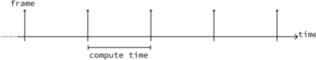
Working in real-time here required to do all the needed operations in a limited time-frame, the one created between two images. This time is defined by the video framerate.
Figure 2: Each frame processing must be done within the time between two frames.
5.4 Specifications
As said, movements were tracked by looking at the limits between the iris and the sclera. It was accomplished by defining groups of pixels on the said border.
Visuals of the principle are listed in the subsection 5.4.1. 5.4.1 Sample image
The figure 11 gives a visual indication of how the border of the iris and the sclera was defined in the system. The iris was simplified into a full black circle and the sclera was reduced to the white area surrounding it.
To detect movements, the median value of groups of pixels near the border was tracked. Therefore, when one median value tends to move away of the black value, it indicated that the target was moving.
To be sure that a movement was actually occurring, a minimum of median values must be out of the defined bounds. Secondary, to be sure that the pixels groups inside in the dark area are valid, a few other pixels groups are placed outside the target and act as control.
By placing those pixels groups in a light area, it became possible to assess if problems occured (invalid video flux for example).
Figure 3 introduce the concept of ROI with the squares. It defines an interesting group of pixels. More information can be found in the subsection 5.4.2.
5.4.2 ROI
On this video flux, up to 32 ROI could be placed. One ROI is defined as a square of 3 to 8 pixels wide (see figure 4), a flag assigned to the ROI that would indicates its mode (inverted or not, explained below) and a X/Y position within the VGA frame. A ROI in its normal operation works inNORMAL MODE. It meant that the detection was
based on a dark base deviating towards clear tones. TheINVERTED MODEwas defined as its exact opponent. The
Decomposition 26.08.2019
Figure 3: The final image processing was based on the following of several pixel groups. It intended to track the movements of the circular target by looking at the median luminosity of specific pixels groups, called ROI.
Figure 4: One ROI is a square between 3 to 8 pixels wide.
Attention must be drawn on the fact that the system must handle a ROI of only 1 pixel even if this is not encountered in real working conditions. This is a tested specification.
5.4.3 What to detect
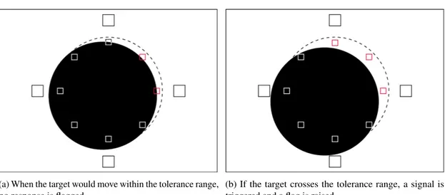
The figure 5 shows how the movement was detected. A red ROI indicated a trigged one.
ROI are used to track movement when placed inside the dark circle and as a control group when placed outside, in the white area.
5.5 Principle of detection
An invalid ROI was defined by a too high medians value (or too low if it was in inverted mode). Mathematically, this was translated as the sum of all pixels within the ROI frame, divided by the number of pixels.
5.5.1 Video
The video flux was in VGA format (640/480 pixels), up to 500[FPS], grayscale 8-10 bits (parametrizable but defined on 10 bits for the thesis) on the LSB of a 16 bits value.
Alternatively, video flux could be provided by a standard Raspberry Pi camera which gave 1080 30[FPS], 720 60[FPS] or VGA up to 90[FPS] [15][16].
Planning 26.08.2019
(a) When the target would move within the tolerance range, no response is flagged.
A red square indicates a trigged ROI.
(b) If the target crosses the tolerance range, a signal is triggered and a flag is raised.
Figure 5: Example of how the target movements were detected. The centred position of the target is indicated in dotted lines.
6 Further steps
An investigation of images transfers via DMA could lead to a more efficient usage of resources.
7 Planning
A simple planning was extrapolated of the analysis in appendix B.
Preparing the whole system and analysing it was planned on 6 weeks, including hands-on. Working on basic task was estimated on 3 weeks.
Finally, implementing the real-time operation was estimated to take 6 weeks as it constituted the central task. In temporal terms, this decomposition looks like the following Gantt-Diagram.
Time in weeks Initial analysis 3 Hands-on 3 PS-PL interactions 3 Real-time operations 6 34/15 32/13 31/12 33/14 25/6 26/7 27/8 28/9 29/10 30/11 24/5 Week number current/in project 20/1 21/2 22/3 23/4
Table 1: Initial planning.
The initial analysis intented to decompose the work into a handful1of main tasks and thinking about how to
implement and achieve them. It also contained the VM setup.
The hands-on one was dedicated to be comfortable with the development environment.
Finally, the main task was divided into two versions. One to work on a reduced and simplified system to outline the problematic and then a second with the real-time operations was implemented.
Hardware 26.08.2019
Part II
Design environment
The design environment was composed by the hardware and the software and the work done is described in following sections.
8 Hardware
Several boards could be used in this study.
As discussed during the introduction meeting, three boards met the needed requirements: • FPGARackZynq[1], a board from HEI
• Snickerdoodle[2], a really compact board
• ZynqBerry[4], a board with a Raspberry Pi form-factor
All of them are based on Zynq 7000 family but are available with different types of core.
Similarities stand in a PS composed by one or two Cortex A9 with FPU and a PL equivalent to Artix-7 FPGA family. More details are available in the Xilinx documentation, see appendix A.
8.1 Board choice
All three are based on a Zynq 7000 serie, therefore, their performances are similar. Slight difference appeared in peripherals and support.
The peripherals were not significant choice criteria as they were not important for this project. Except for the DDR which could be used in a particular use case that was not part of this work.
Having DDR could be useful if the system had to locally store a few images. In theory, the PS was fast enough to get the stream correctly.
If not, the PL must have had a direct access to a dedicated DDR.
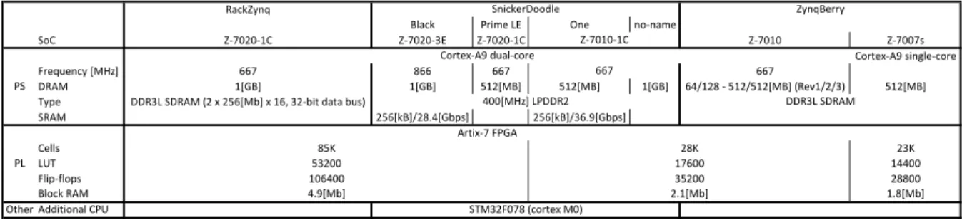
The following table compares briefly the characteristics to choose the board.
RackZynq
Black Prime LE One no-name
SoC Z-7020-1C Z-7020-3E Z-7020-1C Z-7010 Z-7007s Cortex-A9 single-core
Frequency [MHz] 667 866 667 667
DRAM 1[GB] 1[GB] 512[MB] 512[MB] 1[GB] 64/128 - 512/512[MB] (Rev1/2/3) 512[MB] Type DDR3L SDRAM (2 x 256[Mb] x 16, 32-bit data bus)
SRAM 256[kB]/28.4[Gbps] 256[kB]/36.9[Gbps]
Cells 23K
LUT 14400
Flip-flops 28800
Block RAM 1.8[Mb]
Other Additional CPU PS PL 5320085K 106400 400[MHz] LPDDR2 4.9[Mb] 2.1[Mb] DDR3L SDRAM SnickerDoodle Cortex-A9 dual-core STM32F078 (cortex M0) Artix-7 FPGA Z-7010-1C 667 28K 17600 35200 ZynqBerry
Table 2: Characteristics of the suggested boards. A void cell indicates missing information from the manufacturer. As no board disposes of separated DDR, the ZynqBerry, mounted with a 7Z007s, was chosen for its direct availability in the school.
Furthermore, this board was easy to handle and work with as it only needed a µUSB cable to power and program it. Finally, its form-factor was a plus to easily add functionalities such as the official Raspberry camera instead of a dedicated one, direct access to storage via SD-Card-card, HDMI port and other standard as the hardware was designed in this direction.
Virtual Machine 26.08.2019
9 Virtual Machine
To be able to work in a portable and dedicated environment, all the software components were installed in a VM. The chosen environment was composed by the following main components listed in table 3.
Type Software Version Note Ubuntu 18.4.3 LTS VirtualBox 6.0.8 ModelSim 10.7c HDL Designer 5.05-015 Vivado 2018.3 Typora 0.9.74 beta Atom 1.40.0 MediaWiki 1.32.1 git 2.17.1 GitKraken 6.0.0 OS related Design Documentation Version control
Table 3: List of the VM components and version used. The complete instructions are given in appendix C.
During the initial meeting it was defined to work on a Linux based system and Ubuntu was chosen because of its popularity.
VirtualBox was chosen because of its popularity and associated documentation was available . Design tools were defined by school licences and hardware requirements.
Version control and documentation tools (Typora, Atom, MediaWiki) were described as essential and are popular amongst the informatic tools development community. Typora is a Markdown editor which give a nice what you see is what you get paired with an easy to use interface.
Finally MediaWiki was suggested in the initial meeting to host the VM configurations and generics information’s.
9.1 Setup
Shortly, VirtualBox was used to host a near naked Ubuntu. Where additional tools could be introduced. Instructions from Mondzeu Wiki2have been followed to install HDL Designer.
Then ModelSim by similar method3and finally Vivado.
9.2 Hands-on
To test the setup and get an insight of how the environment works, a simple example provided by Digi-Key[7] was followed. This design applies a PWM with a variable duty-cycle driven by a hardware timer on a GPIO and prints some words through serial port.
The VM did not let the serial transmission pass between the board and the environment. As this was not essential, no further investigations were made in VirtualBox configurations.
The facts that the GPIO was reacting and measured with an oscilloscope was sufficient to validate the development chain.
Implementation 26.08.2019
Part III
Loopback
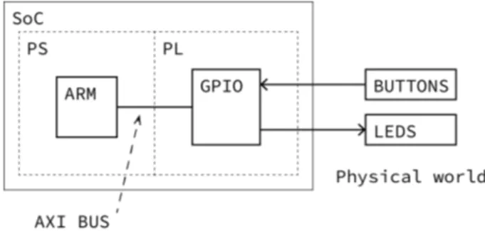
To assess the communication between PS and PL, a form of loopback was implemented.
Taking the form of connecting LEDs and buttons to the processor and linking them via the PL before accessing through AXI to their belonging registers.
Figure 8 gives a simplified schematic view. The GPIO IP is configured with two channels each one dedicated to buttons, respectively LEDs.
Figure 6: Simplified view of PS and PL interaction. The processor can access to buttons state via the logic and the AXI bus.
10 Development basis
Working with the hardware was facilited by a minimal working example easily editable in Vivado.
Based on the previously followed tutorial (see subsection 9.2) which make a LED fade-in and out with a hardware timer, it has served for the loopback task.
11 Implementation
Added to the basis, a GPIO IP was added from the Xilinx libraries. It was parametrized with two channels, one for LEDs and one for buttons, it allowed the PS to access the physical components through the PL.
The implementation was trivial as it consisted of reading GPIO dedicated to buttons and write the value into the registers of LEDs GPIO.
11.1 Specifications
Figure 7: LEDs are driven by GPIO This IP was configured with two channels, one for buttons and one
for LEDs.
Channel 1 was dedicated to buttons,WIDTHparameter = 4 (one bit per
button).
Channel 2 was dedicated to LEDs,WIDTH= 7 (one bit per LEDs but LED
0 was dedicated to the PWM). Interruption was not used.
LEDs Physically, the connections were done as shown in figure 7. The first LED was driven by the PWM from the hands-on, then the next four
Implementation 26.08.2019 used.
The wanted behaviour was button pressed leads to a LEDON thenOFF
when released.
11.2 Hardware design
To fulfil the desired requirements, the block design shown in figure 8 have been implemented.
Figure 8: Block design implemented for working with LEDs and buttons. The block named AXI GPIO was the centre of this design by allowing the PS to interact with external hardware through PL. (source: Vivado block design explorer)
Consisting of two families of blocks, this design allowed an interaction of the PS with external hardware through PL.
The software within the ZYNQ 7 PROCESSINGSYSTEMblock reacted to the buttons push (more information in
subsection 11.3).
Blocks ZYNQ 7 PROCESSINGSYSTEMand PROCESSORSYSTEMRESETwere mandated to use the processor and AXI INTERCONNECTto use the AXI bus.
The only required action was to configure the PS as needed (and already done as this was a common part with the empty architecture realised previously in the hands-on, see subsection 9.2).
GPIO As explained in subsection 11.1, this IP was configured in dual-channels to read and write buttons, respectively LEDs.
11.3 Software
The software was constantly reading the GPIO buttons’s registers to acknowledge when a button is pushed. Then it wrote the buttons status into the register dedicated to LEDs.
Analysis 26.08.2019
Part IV
Real-time processing
12 Analysis
As explained in the initial analysis (see subsection 5.4), the tracking was based on following the state of ROI.
12.1 Processing goal
As said in the introduction, the objective was to track the movements of an eye, which could be schematized as a black target in a white environment as shown in figure 9.
Figure 9: An eye could be seen as a black on white target.
12.2 Application
In reality, an eye is not perfectly black and white. Hence the real coloration of the iris and the sclera can be evaluated on a greyscale.
Factors such as patient himself, exposure time, illumination and angle of view could induce a lighter black (or darker white).
Detection threshold was a parameter proper to each ROI.
As well, ROIs could be placed on a clear environment to detect a decreasing luminosity. In this case, it was working in inverted mode.
Those parameters are shown in figure 10.
Figure 10: An ROI was composed by a position in X/Y and a size as shown here. A non-represented feature was the threshold to which the median value will be compared to, the mode and an id were the remaining characteristics.
Processing 26.08.2019
Figure 11: The final image processing was based on the tracking of ROIs. Their placement showed in this figure is an example. In reality, their positionning and number are user defined.
12.3 How to
In facts, the processing of each ROI was done in one dedicated bloc. It means that for n-ROIs, n-blocks were generated in parallel and data were dispatched by a monitor.
12.4 Optimisations
12.4.1 ComputationsThe calculations to get a ROI value included a division (as the median is defined as the sum of all pixels divided by their quantity).
As divisions were consuming high amount of logic and are inefficient operations in HDL the median was not calculated. Instead, thresholds were given multiplied by the ROI’s pixels amount.
13 Processing
One block computes one ROI. Composed by a state-machine and a few processes, its interface is shown in figure 12. It takes ROI parameters and frame data to do the desired computations namely accumulate each pixel value and confronting it to the given threshold.
13.1 Description
The system is based on a state-machine which drives some counters to count pixels. Then a few processes make the effective ROI detection.
Two processes driven by a counter and the frame signals counted the pixels for a third process which took care of checking if the current pixel was in the ROI. If yes, the value was transmitted to an accumulator before being confronted to the threshold to determine validity.
Proof of concept 26.08.2019
Figure 12: This block takes a ROI and return the according result. It is composed by subblocks which are dedicated to specific tasks.
14 Proof of concept
To validate the global design, a first version which worked on only one data line has been implemented. Using the test benchBASIC PROCESSING(see subsection 17), it was state-machine based.
The top level was the same as in figure 12 unlike there was only one data line. The code for this version is contained within one file available in appendix D.6.
14.1 State machine
Each time a new frame is received, the computation will begin, and this event launches a state-machine which goes as shown in figure 13.
Figure 13: Proof of concept state-machine. A new frame launches the detection and then each time a ROI pixel is found, its value is accumulated. The cycle continue until each pixel has been accumulated.
In a few words, the system behaves as following.
Waiting a new frame is done inIDLEand when a start of frame occurs, it goes intoSEARCH PIXELS. This state launches the search and wait for an indication of a pixel located in the ROI. Then the value is accumulated, and the cycle repeats itself until the last ROI’s pixel.
At that moment, the output is set at the right value, depending of the ROI median value confronted to the threshold and the system is ready for a new frame after being pass throughFINISHED.
Proof of concept 26.08.2019
IDLE This state wait for a start of frame.
SEARCH PIXEL Begin the search by enabling a main counter and waiting for a flag which indicates that a pixel
located in ROI is detected to go in the next state. The search itself is delegated to a combination of processes (see further) driven by the state machine and the main counter.
ACCUMULATE VALUE When entering this state, a flag is raised to enable an accumulator located in a process. If the pixel is the last of the ROI, the state machine will go in the last state, else it will continue the search by returning to the previous state.
FINISHED When the entire ROI is scanned, this stage disables the main counter and indicates the validity of the outputs by rising valid.
14.2 Processes
The state machine uses a few processes to perform actions.
Three of them are dedicated to counting bits and pixels, one detects if the current pixel is in a ROI or not, one accumulates values of ROI’s pixels and the last one verifies if the ROI is valid or not.
COUNTINPUTFLOW Described as main counter, this synchronous reset/clock process counts the incoming bits to synchronize the data flow with the pixel’s counters.
Counts on a base of a constant defining the data duration (in clock cycles). This counter reset its value when not receiving frame, or by a global reset.
COUNTPIXELX Asynchronous process driven by the main counter and the frame signals (start of frame and start
of line) to count the pixels in x-axis.
Increment itself when the main counter reaches its half-period (arbitrary timing, parametrizable). This counter reset its value when a global reset or a new frame occurs and on every new line.
COUNTPIXELY Similar to the x-axis counter but driven by start of line to increment itself. This counter reset its value when a global reset or a new frame occurs.
DETECTPIXEL Synchronous reset/clock process which check if the actual pixel is in the ROI or not. This is done by confronting its coordinates to the counters x/y every time that a new pixel was incoming. This is known by checking changes on the x-axis counter.
When a wanted pixel is detected, its value is stored in a buffer and a flag is raised for the state machine.
It is also detecting when the actual pixel is the last to be buffered, there too by rising a flag intended to the state-machine.
ACCUMULATE_PROC Combinatorial process which accumulates given pixels values in a buffer.
When a new frame occurs, resets itself.
CHECKVALUE Combinatorial process which was triggered when the ROI’s last pixel is detected. Confronts the accumulator buffer to the threshold and returns a logic response.
VGA processing 26.08.2019
15 VGA processing
The main difference with previous data format occurs in transmission, as VGA format is given through eight parallel lines instead of one.
One frame is transmitted by batch of 8 pixels on 8 data lines, meaning that between two batches, each pixel must be checked to see if it is comprised into a ROI.
This leads to a more complex design which is not anymore hidden in one block but divided to get an easier and clearer view.
Figure 14: COMPUTEROI is composed by a state-machine which drives the tracking, some counters to search
pixels, several blocks to get the right values and finally an accumulator/comparator to deliver the result. Figure 14 show the new repartition of tasks into the blocks.
Principle is the same, counting incoming data and extract from this pixel’s values and coordinates, driven by a state-machine. Analysing if any of the pixels could be in ROI and then buffer interesting values.
Finally, an accumulator will add-up and check if the value is above or not of the given threshold.
15.1 State machine
In this second iteration, the state machine is reduced in three states as the accumulation is done by a dedicated sub-system.
Figure 15: To work with VGA and its 8 input data lines, the state machine has been simplified as some of the work is done in driven subblocks.
VGA processing 26.08.2019
15.2 Pixel counters
To synchronize and receive correctly the incoming pixel flow, a block is dedicated to counting and indicating when values are ready to be read and what they correspond to.
Figure 16 show the chronogram of inputs and output signals.
Figure 16: Chronogram ofPIXEL COUNTERS. Taking as input data lines and frame signals, it delivers two counters
to know where in the frame the incoming pixels are and when they are ready to be read. Clock is not represented as it is much faster than those signals.
On each new batch of pixels, the x-counter increments itself by step of data lines number (in this case 8) and on every start of line the y-counter does the same. Due to this sensibility to the signal, this second counter starts on 1 instead 0 as x-counter.
Another way to do could be to increment the counter in y-axis when the x-axis reaches the end of a line. This has the main disadvantage not to be anymore resynchronized with the incoming flux by start of line. Finally, new pixels indicate when a batch is ready to be read in the input buffers to be read by following blocks. A start of frame reset all counters and flag to 0.
The code is available in appendix D.8.
15.3 ROI tracker
This block provides indication of when the incoming pixels contains some of the ones from the ROI to track and when the last ROI pixel is arrived. Those information’s are encoded in signals in ROI and last pixel.
The two other signals (offset x and overlap) are employed to get the right pixels in each batch.
Figure 17 and 18 show the different situations of how a ROI could be positioned within the received pixels. Next paragraphs detail the tasks of the implemented processes.
Figure 17: First situation, ROI is fully contained by a batch of pixels for each of its line. In this case, the offset x is defined as the number of the first pixel to match with ROI.
VGA processing 26.08.2019
COMPUTEOFFSETS In the case shown in figure 17, each line of the ROI is fully contained by a batch of pixels. It means that an offset in x (and y but this axis is much more intuitive as it increments itself on each new line as soon as a ROI is detected until its end) must be computed to accumulate the right values further in the logic (see subsection 15.4).
Processing those offsets is the task of the processCOMPUTEOFFSETS.
Figure 18: Second situation, ROI is partially over a second batch of pixels. It means that for the current batch all pixels after the offset must be taken into account in accumulator but also a few from the next batch. The remaining amount is given by overlap value.
A difference exists between offset x and offset y. The first one is used by other blocks (see subsection 15.4) but offset y is only an internal signal used by the ROI tracker processes.
DETECTOVERLAP The second case shown in figure 18, the current batch in now on the second ROI line and overlapping over two batches.
At this moment, the processDETECTOVERLAPis useful to indicate that an overlap is occuring and gives its size. To be exact, a signal overlap is set to the right value if this situation occurs, else it stays at 0.
Again, those information’s are used further in the logic in the pixel tracker.
DETECTROIandDETECTROIEND The two remaining processes are pretty similar. They intend to detect the
first, respectively the last, pixel of the ROI. The code is available in appendix D.10.
15.4 Pixel Tracker
This block in generated once for each data line and is dedicated to check if its specific pixel value is to transmit to the accumulator. Figure 19 shows a simplified schematized view of how each pixel is read by the trackers. The enable signals comes from a trivial logic which use offset x, inRoi and overlap signals from ROI TRACKER.
Figure 19: The logic functionality of the pixel tracker is a logic switch which transmits either the pixel value or a 0 if it is not a ROI.
Libraries 26.08.2019
Figure 20: In this situation, the current batch contains three pixels in a ROI, 5 to 7 shown in dark grey. It means that the enable from trackers 5 to 7 are activated.
Figure 20 show an example of how the trackers transmit or not the pixels values to the accumulator. The code is available in appendix D.9.
15.5 Accumulator
The accumulator is in charge of taking the buffered pixels values and sums them up into another buffer. The maximal value that could occurs is defined as in equation 1.
accumulatormaximal=ROI2size·pixelbitdepth=82·216=222→22bits (1)
Practically, the pixel value is encoded on 10 bits which are then stored in 16 bits values. Hence, it limits the maximal value to 16 bits as shown in equation 2.
accumulatormaximal=ROI2size·pixelbitdepth=82·210=216→16bits (2) Based on aFOR LOOParchitecture which generates an accumulation of each input buffer in a variable, it will, after
those operations, confronts the accumulated value to the given threshold.
Comparison is quite simple, either the ROI is in normal or reversed and hence, the final result is a binary response.
ACCUMULATOR This process accumulates the value of its input data line each time a new batch of pixels is ready. The previous blocks (pixel trackers), transmit to the accumulator a 0 by default or the pixel value if it is a pixel from a ROI.
Hence, this process is trivial as it could always accumulate all its inputs. In facts, it is some expanded logic with a
FOR LOOP.
CHECKTHRESHOLD When an end of processing is thrown, the process compares the accumulated value to the
given threshold. ROI mode (inverted or normal) are also considerated. The code is available in appendix D.7.
16 Libraries
All codes used in this work originating from the libraries defined by LIBRARYIEEE, especiallySTD_LOGIC_1164
andNUMERIC_STD.
In parallel, a package was written to define some constants and data types. The package is available in appendix D.12.
Basic processing 26.08.2019
Part V
Test benches
Three tests benches were conceived. One for basic processing, one for final tests and one to unit test the accumulator.
17 Basic processing
A simplified test bench is implemented to perform a proof of concept.
It generates a picture on only one data line, feeding a single ROI tracker and have been used it to validate a proof of concept.
17.1 Objectives
This test bench was designed to fulfill these objectives:
• Generating some data to simulate a frame and feeding of the tested block • Be comfortable with the VGA signals
• Creating a base for more complicated test benches
17.2 Implementation
It was based on a state machine which drives a counter to generate data in the form of a greyscale.
Figure 21: Frame generation is driven by a state machine which draws lines until reaching the desired amount.
GENERATEDATA The data are generated by a counter and boundaries are defined by generics, as well as the step
between two pixels.
Practically, the greyscale is a 10 bits ramp. The pixels are counted line by line and a second counter stops the generation when their requested number is reached.
In parallel of this, a few parameters and signals are generated such as ROI attributes (position in x/y, threshold and mode) and frame signals (start of frame and start of line) as shown in figure 22.
VGA processing 26.08.2019
Figure 22: The basic test bench generates a 10 bits ramp over one data line, the frame signals and set ROI parameters (not shown).
18 VGA processing
18.1 Data generation for global test
To validate this version, the developed test bench must be reworked a bit to concord with the following changes: • Data are splitted on 8 parallels lines
• Each data is a pixel, meaning that each time a new batch of pixels comes, 8 new pixels are coming in series with the last ones
Main changes where done on the way of generating data. Counters counts 8 by 8 (whether the number of data lines) and each line is incremented to match with its relative position in the batch.
Figure 23 show the 8 data lines of this test bench iteration.
Figure 23: The test bench for VGA format generates a 10 bits ramps for each 8 data lines, the frame signals and set ROI parameters (not shown).
VGA processing 26.08.2019
18.2 Unit tests
Not all blocks are individually tested as it takes a lot of time to conceive the tests or it is not useful as their behaviour is trivial and thus verified in global tests.
Ideally, it would be better to tests each block individually but as time was a constraint, choice was made not to implement the tests.
18.2.1 Accumulator
To make tests easier and faster, the accumulator was tested independently with a dedicated test bench. The criteria needed to declared a test as successful are described below:
• transmitting a given ID
• comparing the accumulated value with the threshold • and telling when the result is valid
Transmitting a given ID is a copy of ROI ID to the output. It is later used to sort all the individual results from each compute ROI blocks.
Testing this block alone asks a certain amount of tests given by formula 3 which must be summed with following behaviours:
• when a start of frame occurs, accumulator must reset
• an end of processing leads to confronting the accumulator value against the threshold and so on an indication on output by a binary result. A valid tell when the result is ready.
Those two behaviours can be tested in only one situation.
base = mode ·threshold = 2 · 3 = 6 (3)
Thus, six tests would be performed to validate each case and one more to check both behaviours.
Implementation Consisting of seven cases covering each possibility, the pattern is simple and repetitive. Parameters have been set accordingly to the test case and a loop drive the accumulation. When it ends, the end of processing signal is thrown to test the last accumulator stage, the check against the threshold.
Results 26.08.2019
Part VI
Tests
To validate the system, several tests were performed using the test benches described in part V.
Testing each possibility involves a lot of individuals tests. As a reminder, the main tested characteristics were the following:
• various sizes, from 1 to 8 • both modes, normal and inverted
• median value above, under and equal to the threshold • position near frame borders
• overlap of ROI on multiple incoming pixels batches
Modifying the lines in the listing 1 allows to test the system with the given parameters presented in the abstract bellow. 1 −− s e t p a r a m e t e r s 2 r o i _ x <= t o _ u n s i g n e d ( 6 3 2 , r o i _ x ’ l e n g t h ) ; 3 r o i _ y <= t o _ u n s i g n e d ( 4 7 1 , r o i _ y ’ l e n g t h ) ; 4 roi_mode <= ’ 0 ’ ; 5 r o i _ s i z e <= t o _ u n s i g n e d ( 8 , r o i _ s i z e ’ l e n g t h ) ; 6 r o i _ t h r e s h o l d <= t o _ u n s i g n e d ( 1 0 0 0 , r o i _ t h r e s h o l d ’ l e n g t h ) ;
Listing 1: The five lines to edit to test multiple ROI positions. Value are an arbitrary example. The amount of combinations is given by formula 4. Each label encodes the number of possibilities.
combinations = size · mode ·threshold · overlap · position = 8 · 2 · 3 · 2 · 4 = 384 (4) As said in subsection 18.2.1, a unit test performed on the accumulator reduces greatly the amount of tests to do, as shown in formula 5 it eliminate cases.
combinations = size · overlap · position = 8 · 2 · 4 = 64 (5) Then, only a certain amount of theses combinations must be performed. Remaining tasks would be to test ROI properties (size, position and overlap) but many are redundant.
By example, testing the position near border is in no way related to the ROI size. Indeed, the border could lead to strange behaviour if a ROI is exactly placed on the last pixel, but this appears independantly of the ROI size. The real amount of test is brought down to 20 (see formula 6).
combinations = size · overlap + position = 8 · 2 + 4 = 20 (6)
19 Results
For readability reasons, the whole results table is available in appendix D.5.
All tests have been successfully passed. Overall, the results show that with different initial conditions, the system reacted positively and in an expected manner.
System improvements 26.08.2019
Part VII
Further work and improvements
20 Remaining tasks
20.1 Implementation
The whole system must be converted and integrated into the Zynq to be fed by a real video flux (whether it is originating from a camera or computer).
Due to a discussion with Mr. Corthay it has been decided that integrating the whole system into the Zynq hardware was not necessary as it does not show a real interest in this work.
21 System improvements
21.1 Accumulator
The accumulator is a simpleFOR LOOPover the incoming pixel batch leading to a cascade of accumulator as shown
in figure 24.
The problem is that the path to get to the final result is as long as the number of values to add (complexity O(n) where n is the number of values to sum).
Figure 24: A cascade accumulator work with a serie of additionner.
Balanced tree A possible improvement could be an implementation of a balanced tree.
It is interesting as it reduces the number of additions to log(n) where n is the number of value to sum. Figure 25 show its architecture.
21.2 Test bench
The implementation of the tests benches was a bit rudimentary and showed little flexibility.
A real improvement could be to use the current state-machine based system and drive it with a few parameters such as:
new frame requests a new frame generation, could be paired with a few parameters such as image type (white/black, pattern (greyscale, noise))
roi set ROI parameters
Others improvements 26.08.2019
Figure 25: A balanced tree reduce the length of the path needed to do the full operation and bring parallelisation to the operations.
22 Others improvements
22.1 ROI
By improving the system, one should be able to process rectangle ROI. This could allow a fine placement (and less pixels to monitor) of ROI along the border who could be seen as near linear as shown in figure 26.
Figure 26: A rectangle ROI to get a better fit on the edge.
22.2 Using DMA
To make faster data transfer without overloading the system, the DMA could be used to transfer frames between the tracking system and the processor in the case where the processor needs to receive a video flux.
This consideration should be taken into account when the current system will be integrated into a higher-level architecture.
26.08.2019
Part VIII
Conclusion
As described in part I, this diploma work was defined by the following goals: 1. Put together a Zynq design environment
2. Develop a system where the PS can stream data to a component in the PL which does a very simple task and stream back to the PS
3. Develop a more complex component implementing an image processing task in real-time 4. Investigate the possibilities of DMA for the image transfers
Globally, the defined goals and their evolution were reached.
Design environment The design environment is functional, ready to use and portable via its VM.
Stream from PS to PL and back Streaming data between PL and PS has been modified into an interaction between both parts.
A user interface taking form of LEDs and buttons is connected to the PL and the PS reacts to this interface. Hence, the interaction is located in the register read/write operations.
Real time image processing The system is capable of receiving a video flux and analysing the comportment of a given ROI.
Further work The real-time operations are fully functional in simulation but needs to be synthetized and tested on hardware.
As setting up a whole system is a time consuming task, it has been decided not to implement this feature in this work. See subsection 20.1 to get more details.
A better implementation of the accumulator could give better performance as it shortens the longest path, see subsection 21.1 for more information.
Designing and implementing a higher-level architecture to handle more ROI per frame by generating the needed amount of computing blocks is the next main step.
Finally, implementing a bunch of automatized test benches must be done to validate faster the improvements done.
26.08.2019
Part IX
Bibliography
BIBLIOGRAPHYBibliography
[1] Hardware/FPGARackZynqADDAV1 - UIT. url: http://wiki.hevs.ch/uit/index.php5/ Hardware/FPGARackZynqADDAV1 (visited on 05/13/2019).
[2] snickerdoodle | krtkl. url: https://krtkl.com/snickerdoodle/ (visited on 05/13/2019). [3] Jann Kumann. TE0720 TRM - Public Docs - Trenz Electronic Wiki. Sept. 2018. url: https:
//wiki.trenz-electronic.de/display/PD/TE0720+TRM (visited on 05/16/2019).
[4] Jann Kumann. TE0726 - ZynqBerry - Public Docs - Trenz Electronic Wiki. Wiki. Sept. 2018. url: https://wiki.trenz-electronic.de/display/PD/TE0726+-+ZynqBerry (visited on 05/13/2019).
[5] Shahul Akthar. Block RAM and Distributed RAM in Xilinx FPGA. en-US. Oct. 2014. url: https : / / allaboutfpga . com / block - ram - and - distributed - ram - in - xilinx - fpga/ (visited on 05/16/2019).
[6] KRTKL. krtkl wiki - boards specifications. Sept. 2018. url: https://wiki.krtkl.com/ index.php?title=Main_Page (visited on 05/16/2019).
[7] Getting Started with the ZynqBerry - Motley Electronic Topics - eewiki. url: https : / / www.digikey.com/eewiki/display/Motley/Getting+Started+with+the+ZynqBerry# GettingStartedwiththeZynqBerry-HardwareDesign (visited on 05/21/2019).
[8] Pre-Harvest: Getting Started with the Zynqberry in Vivado 2018.2. en-US. url: https:// www.knitronics.com/the-zynqberry-patch/getting-started-with-the-zynqberry-in-vivado-2018-2 (visited on 05/24/2019).
[9] Altera. “Understanding Metastability in FPGAs”. en. In: (), p. 6.
[10] Eduardo Sanchez. VGA video signal generation. en. url: http://lslwww.epfl.ch/pages/ teaching/cours_lsl/ca_es/VGA.pdf (visited on 07/19/2019).
[11] Vivado Design Suite User Guide: Using Tcl Scripting (UG894). en. 2018. (Visited on 08/07/2019). [12] “Graphical Editors User Manual”. en. In: (2008), p. 482.
[13] “HDL Designer Series User Manual”. en. In: (2008), p. 602.
[14] Peter J Ashenden. Designer’s Guide to VHDL. eng. Morgan Kaufmann, 2008. isbn: 0-12-088785-1.
[15] Camera Module - Raspberry Pi Documentation. url: https://www.raspberrypi.org/ documentation/hardware/camera/ (visited on 08/20/2019).
[16] IMX219PQ | Sony Semiconductor Solutions. en. url: https://www.sony-semicon.co.jp/ new_pro/april_2014/imx219_e.html (visited on 08/20/2019).
[17] Eye color. en. Page Version ID: 910825107. Aug. 2019. url: https://en.wikipedia.org/ w/index.php?title=Eye_color&oldid=910825107 (visited on 08/22/2019).
[18] The World’s Population By Eye Color Percentages. en. url: https://www.worldatlas. com/articles/which-eye-color-is-the-most-common-in-the-world.html (visited on 08/22/2019).
Datasheet 26.08.2019
Part X
Appendix
A Datasheet
To keep a light bibliography, used datasheet are listed here.
Xilinx provide the following documentation to use their environment: • Zynq-7000 SoC Data Sheet: Overview, DS190 (v1.11.1) July 2, 2018
• Zynq-7000 All Programmable SoC Software Developers Guide, UG821 (v12.0) September 30, 2015 • The Zynq Book, 1st Edition, produced in association with Xilinx by the University of Strathclyde, Glasgow Others are available at http://www.xilinx.com/products/silicon-devices/soc/zynq-7000.html#docum entation
Specifications and initial analysis 26.08.2019
B Specifications and initial analysis
A document generated at the project genesis to analyse the given specifications and how the project is dissolved in various tasks.
Video processing on SoC
Bachelor thesis
S
PECIFICATIONS AND INITIAL ANALYSIS
Abstract
The aim of the diploma work is to develop the base for an image processing task on a Xilinx Zynq SoC. In this system, the ARM Cortex-A9 based Processing System (PS) will stream images to the Programmable Logic (PL) which will perform an image processing task on the fly.
Student :
Loic FRACHEBOUD
Teacher :
François CORTHAY
Expert :
Pascal FAURE
From :
HES-SO Valais-Wallis
Contents
1 Design environment 2 1.1 Environment setup . . . 2 2 Basic processing 3 2.1 System architecture . . . 3 2.2 Feedback flux . . . 33 Real time image processing 4
3.1 Specifications . . . 4 3.2 Principle of detection . . . 6
4 Further steps 6
13.06.2019
Introduction
This document intend to detail requirements of bachelor thesis. It is a compenent of the main report and does not constitute a whole independant document itself.
Please refer to the report for any missing information.
Objectives
Basis goals are defined by thesis description: 1. Put together a Zynq design environment
2. Develop a system where the PS can stream data to a component in the PL wich does a very simple task and stream back to the PS
3. Develop a more complex component implementing an image processing task in real-time 4. Investigate the possibilities of Direct Memory Access (DMA) for the image transfers From this each goal is decomposed in a few tasks to get an idea of how the project will take place.
Design environment 13.06.2019
Decomposition
1 Design environment
The first objective is to define a design environment and it begin by defining the development board. During the thesis introduction meeting three boards were suggested:
• FPGARackZynq1, a board from HEVS developped by Charles Papon
• Snickerdoodle2, a really compact board
• ZynqBerry3, a board with a Raspberry Pi form-factor
All three are based on a Zynq 7000 serie, placing them on a similar performance basis. Differences appears in peripherals and support but nothing really big.
After a discussion with Mr. Faure, the ZynqBerry with a 7Z007s available at school will be sufficient.
1.1 Environment setup
The work will be done within a VM. It allocate a nice portability of the project and a light working environment in term of just having what is needed.
It will be composed mainly as following: 1. Ubuntu
2. Vivado 3. HDL Designer
4. Atom, git and such useful tools
The exact list of tools will be defined on setup and especially while working with it.
1http://wiki.hevs.ch/uit/index.php5/Hardware/FPGARackZynqADDAV1 2https://krtkl.com/snickerdoodle/
Basic processing 13.06.2019
2 Basic processing
This will be decomposed in a few milestones: A. Setup a simple stream from the PS to the PL B. In the PL, forward the stream back to the PS
C. Do a simple operation on the stream before sending back
2.1 System architecture
The first step takes as input a top level design from Mr. Faure wich gives a few IP to fastly get a working design as shown in figure 1.
This define an architecture where the PS stream a data flux to the PL and require to specificate how and in wich format the data is transmitted.
Figure 1: System architecture, the block named Processing contain more IPs and especially the one in which my system will take place.
Then from the PL point of view, the stream must be recovered and forwarded back to the ARM. This validate the communication between PS and PL.
Finally, a simple operation such as bit inversion will be performed on the stream.
2.2 Feedback flux
To give a feedback, a slower flux must be given back to the PS.
This could consitute a nice work to do at this moment because the data flows are proved working with really simple operation.
Generating this feedback consist in reducing the framerate on a lower value.
This value could be a fixed parameter or dynamically processed from the original framerate to obtain the wanted one.
Real time image processing 13.06.2019
3 Real time image processing
Later a more complex operation on the stream will be performed. A. Start by a simple operation in real time
B. Develop a more complex processing to perform image processing Working in real time with image processing is the main objective.
To reach it, real time operations must be implemented. At this point, odds are high that the simple operation implemented previously is working in real-time.
Finally an image processing operation will be conceived to be applied on the stream.
Working in real-time here ask to do all needed operations in a limited time-frame, the one between two images.
Figure 2: Each frame processing must be done within the time between two frames.
3.1 Specifications
Video The video flux is in VGA format (640/480 pixels), up to 500[fps], grayscale 8-10 bits on the LSB of a 16 bits value.
Some informations are available in registers, others are given as hard parameters. This will be more preciselly defined when the architecture will be in my hands.
ROI On this flux, up to 32 ROI could be placed. One ROI is defined as a square of 3 to 8 pixels wide (see figure 3), a flag who indicates its mode (inverted or not, explained below) and a X/Y position inside the VGA frame. A ROI in it’s normal operation works in normal mode. It means that the detection is based on a dark base deviating towards clear tones. The inverted mode is it’s exact opponent. The ROI is trigged by a deviation from clear to dark tones. The application of both modes is given below.
Figure 3: One ROI is a square between 3 to 8 pixels wide.
Later it could be nice to improve the system to be able to process rectangle ROI. This to allow a fine placement (and less pixels to monitor) of ROI along the border who could be seen as near linear as shown in figure 4.
Figure 4: A rectangle ROI to get a better fit on the edge.
Be aware that the system must handle a ROI of only 1 pixel even if this is not encounter in working conditions. This is a tested specification.
Real time image processing 13.06.2019 Sample image The figure 5 gives a visual indication of how it looks like.
In the center, the circle is the target to follow. If it moves, this has to be indicated. The circle is really dark, close to full black.
To detect movements, ROI are placed inside the target along the border. So when one ROI median value tends to move away of black, it indicates that the target is moving.
Validation of a movement needs a minimum amount of ROI trigged, given as a parameter.
Secondary, to be sure that the ROIs in the dark are valids, a few inverted ones are placed outside the target. As this area is well lit, if they are not bright it means that a problem occurs (invalid video flux for example) and it must be indicated as well.
Figure 5: The final image processing is based on the following of thoses ROI. It intend to track the movements of the circular target by looking at the median luminousity of the previously placed ROI.
What to detect The figure 6 shows how the movement is detected. A red ROI indicates a trigged one.
(a) When moving a little, ROI are detecting it (in red are the triggered ones) but the threshold is not overpassed (in this example there is not enough ROI triggered to indicate a movement).
(b) If the target is moving too much, the threshold is over and yet the system must halt.
Planning 13.06.2019
3.2 Principle of detection
An invalid ROI is defined by a too high median’s value (or too low if it’s in inverted mode). Mathematically this is translated as the sum of all pixels within the ROI frame, divided by the number of pixels.
A monitoring system will then take as input the median value of all ROI and if their number exceed the threshold, it will be indicated.
4 Further steps
An investigation of images transfers via DMA could lead to a more efficient usage of ressources. This need to be thinked when the system is proved.
5 Planning
A fast planning is extrapolated of this analysis. A much more detailled will be generated and available with the report.
Preparing the whole system and analysing it is planned on 5 weeks. Working with the flux and doing the simple loop is estimated on 2 weeks.
Finally, implementing the real-time operation must take 7 weeks as it constitute the central task.
VM setup 26.08.2019
C VM setup
Preparing a design environment
Begin by installing an Ubuntu as a VM. Disk space must be at least 50[GB] (Vivado is quite big). Continue with a few useful tools such as git and Atom.
A shared folder between Windows and Ubuntu could be nice. When needed it could mounted with the third command below (automount disabled to keep portability as high as possible with very little configuration when runned by another HW).
Install HDL Designer
Follow http://mondzeu.ch/wikis/EDA/index.php?title=Install_HDL_Designer
HDS_2018.1_ixl.exe is given by M. Corthay
Library files weren't copied HDL Designer is called directly in
A few things were added to /etc/profile
Configure HDL Designer
A project is created based on one of the 6th semester lab. A few configurations occurs in the *.bash files.
First take the /Scripts and /Syntax folder from one of them and the project_name.bash file.
Granting a 775 access is needed (full power to the owner and the group (Read-Write-Execute) but only RE to other) for the project folder and the /Scripts.
Rename all to the desired name and especially replace all old occurence of the old project name in the project_name.hdp file located in project_name/Prefs. This file make the link between
mkdir ~/shared
sudo adduser bachelor vboxsf
sudo mount -t vboxsf vm_share ~/shared
/usr/opt/HDS_2018.1/bin/hdl_designer
#--- # EDA tools
#
export PATH=$PATH:/usr/opt/HDS_2018.1/bin:/usr/opt/Modelsim/modeltech/bin
export
Be aware that if HDL Designer installation folder is different of HDS, it must be changed in
hdl_designer.bash file located in /Scripts. This could be improved in the long-run by setting a
variable who define the folder exact name for the entire script.
Install ModelSim
Follow http://mondzeu.ch/wikis/EDA/index.php?title=Install_Modelsim
A difference occurs at the "Install after HDL designer" step. I've done the following instead.
Testing ModelSim was done from the /bin directory
If one of the PATH variable is not found, export it.
Install Vivado
The installation take place with Design Edition in /usr/opt/Xilinx without packages for Zynq
Ultrascale.
Vivado need Gtk package:
And must be launch as root
Configure a Vivado project
Those two following links give a nice overview on how start and work with the environment :
https://www.knitronics.com/the-zynqberry-patch/getting-started-with-the-zynqberry-in-vivado-20 18-2
https://www.digikey.com/eewiki/display/Motley/Getting+Started+with+the+ZynqBerry
Basically consisting of downloading board files and creating a project based on this board.
Steps for the first run
Being by following the DigiKey tutorial (with a Z7007s chip in my case) until Standalone Software
Design. Here jump to the Knitronics tutorial.
Then some code lines must be commented out in main.c (301-311 in my case), edit DDR base
address to 0x0 on line 35 of xparameters.h (pointed by line 296). Optional but recommended
for debugging, the lines 291-294.
sudo ./install.aol/mgc_install &
sudo ./usr/opt/Modelsim/modeltech/bin/vsim &
sudo apt install libcanberra-gtk-module
After, the tutorial recommend a few modification in the Hello World program but I won't use it, so just ignore it and fly back to the DigiKey one on Application Code.
Take the application code and replace all the content of main.c with it.
This tutorial then give a few instruction on UART (Modify BSP settings), as it's not used, ignore it. Set the run configurations as explained just above the given application code and especially, set
Run ps7_init and Run ps7_post_config as sometimes the system is held in reset.
From there, it must apply a dynamic PWM in the sense of a variable going forth and back from 0 to 100% on the GPIO7, visible on oscilloscope.
Steps for a new iteration
Apply again the configuration file to ZYNQ PS block and keep desired peripherals (in this case UART 1, MIO 48-49)
Run synthesis, implementation and generate bitstream Export Hardware (file -> export -> export HW) with bitstream Launch SDK
Run configuration which do a full system reset
MediaWiki
Follow http://mondzeu.ch/wikis/mediaWiki under Installing to have a full install procedure. The folder in wich the Wiki will be installed must be editable by user.
Then the index.html must be loaded before the PHP one. This is configurable in lighttpd.conf.
Appendix
Resize partition
As the program need around 40[GB] I had to resize the VM. I choose 100[GB] to have a bit of spare space.
A GParted VM has been set to resize the partition. This second VM take the *.vdi from the first one as a SATA device.
Then just run GParted, extend the partition and apply.
chown -R bachelor:users www
cd C:\Program Files\ Oracle\VirtualBox
VBoxManage modifiyhd "C:\Users\loic.frachebo\VirtualBox VMs\bachelor\bachelor.vdi" --resize 100000