HAL Id: hal-03174553
https://hal.archives-ouvertes.fr/hal-03174553
Submitted on 19 Mar 2021HAL is a multi-disciplinary open access archive for the deposit and dissemination of sci-entific research documents, whether they are pub-lished or not. The documents may come from teaching and research institutions in France or abroad, or from public or private research centers.
L’archive ouverte pluridisciplinaire HAL, est destinée au dépôt et à la diffusion de documents scientifiques de niveau recherche, publiés ou non, émanant des établissements d’enseignement et de recherche français ou étrangers, des laboratoires publics ou privés.
s-SNOM imaging of a THz photonic mode
Théo Hannotte, L. Thomas, Benjamin Walter, Mélanie Lavancier, Sophie
Eliet, Marc Faucher, J.F. Lampin, R. Peretti
To cite this version:
Théo Hannotte, L. Thomas, Benjamin Walter, Mélanie Lavancier, Sophie Eliet, et al.. s-SNOM imaging of a THz photonic mode. 2020 45th International Conference on Infrared, Millimeter and Terahertz Waves (IRMMW-THz), Nov 2020, Buffalo, United States. pp.1-2, �10.1109/IRMMW-THz46771.2020.9370928�. �hal-03174553�
s-SNOM imaging of a THz photonic mode
T. Hannotte1, L. Thomas1, B. Walter2, M. Lavancier1, S. Eliet1, M. Faucher1, J.-F. Lampin1 and R. Peretti1
1Institut d’Electronique, de Microélectronique et de Nanotechnologie, CNRS, Univ. Lille, Villeneuve d'Ascq, 59652 France
2Vmicro SAS,
Villeneuve d’Ascq, 59650 France
Abstract :
We report on the imaging by THz s-SNOM of the field concentration associated to the photonic mode of a split-ring resonator with a 2 µm small gap. The ability to concentrate and probe THz radiations at this scale is of interest for studies on micro and nano objects. Our results are interpreted with numerical calculations as an interplay between the confined near-field and the directional far-field emission of the system.
Introduction :
Confinement of THz electric fields in small volumes is highly desired to investigate light-matter interactions at sub-λ scales, typically < 100 µm [1]. This is specifically salient for both applied and fundamental purposes. For instance, one can use the field confined in a THz resonator to sense a single nano object placed in a gap of the resonator [2], or to enhance interaction with 2D material to build THz modulators [3] or, on the fundamental side, to enable ultrastrong light-matter interaction at sub-wavelength scale in the THz domain [4].
Such confinement is achieved using THz resonators. In addition to their collective effect on electromagnetic waves, individual resonators often concentrate electric field in gaps as small as a few 10 nm [5] leading to very important field confinement in terms of Purcell’s factor when their eigenfrequency is tuned to the incident radiation.
As a consequence, an in depth qualitative and quantitative knowledge of both the metasurface and resonators is an important prerequisite for most of these studies. Since more than 10 years, several groups worldwide put effort in developing THz scattering Scanning Near-field Microscopy (s-SNOM) for this purposes. s-SNOM uses the apex of the tip of an Atomic Force Microscope (AFM) operating in intermittent contact mode as a nano-scatterer used both to couple the THz beam in the resonator and the field of the resonator to the far-field. This technique determines both the radiative and the non-radiative near-field (NF) distribution with a sub-λ resolution while imaging the
topography of the sample [6]. However, despite its importance and all the efforts put in, direct characterization of confined THz photonic modes in the NF at such scales remains limited.
In this work, we explore the limits of photonic mode near field imaging by studying the NF distribution of the electric field in split-ring resonators (SRRs) with a THz s-SNOM. We use a probe specifically designed for efficient THz scattering and we propose a physical explanation accounting for the differences between our result and the expected field profile.
Key elements design :
The main elements of a s-SNOM experiment are the sample, the probe, and the optical setup for illumination and detection. We use a standard optical setup and the neaSNOM platform similar to the ones presented in [6]. Here we focus on the design and fabrication of the most significant elements for our problematic: the resonator and the scanning probe.
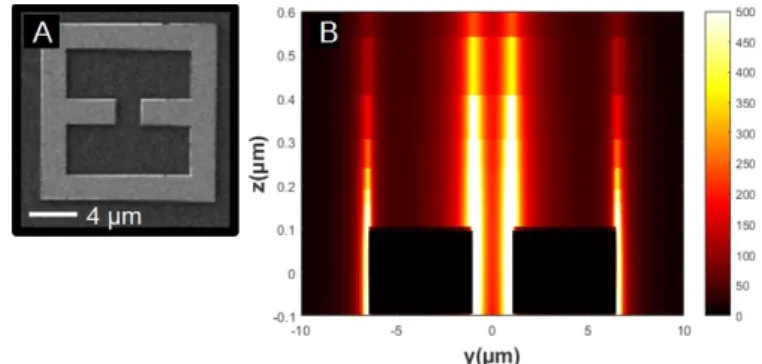
The chosen geometry for our resonator is a double loop SRR (fig. 1A). We use high resistivity silicon substrate for its low absorption and low dispersion in the THz range [7]. Electromagnetic simulation with FDTD predict the confinement of the electric field in the gap and its extension to the branches of the capacitive element atop the device. Since a s-SNOM tip is can be modelled as a vertical dipole antenna, we will only consider the electric field projected on the vertical axis (fig. 1B). We fabricated the SRRs following the process described in [8]. Figure 1A shows a SEM picture of one of the fabricated SRRs.
The s-SNOM tip used for all the experiment was a Lprobe model ‘CT’ from Vmicro [9]. This probe is especially designed for THz s-SNOM experiment. In fact, Maissen et al. demonstrated that the imaging resolution can be greatly increased by using long and ultrasharp s-SNOM tips, and achieved resolution down to 15 nm [10]. Additionally, s-SNOM tip can be modeled as a dipole antenna excited by the near field concentration on the sample; hence, a longer tip (close to the excitation wavelength) will have a better scattering efficiency despite the small apex. The Lprobe aims at coping with these issues.
The fabrication process of such probes differs from all other commercially available cantilevers. The Lprobes are fabricated on a SOI (Silicon On Insulator) wafer. The cantilever and the tip are fabricated in the wafer plane, in the Device Layer (Dl) which is the top silicon layer of the SOI wafer. The fabrication process gives access to a wide range of cantilever parameters regarding the resonant frequencies and stiffnesses as well as tip geometry. In this work, the angle between the tip and the cantilever is 100° and the tip length is 70µm (fig 2A-B). In figure 2C, we present the simplified process flow implemented by Vmicro : i) Initial cantilever patterning with photolithography and plasma etching. ii) Oxide hard mask deposition. iii) Anisotropic chemical etching of the silicon using a KOH solution. The chemical etching stops on the <111> plane. iv)
Oxide hard mask removal using an HF acid solution. v) Back side plasma etching defines the AFM chip. vi) Final HF etching of the buried silicon.
On figure 3B, we present the fabricated cantilever with up to 70 µm long tips. Getting back to the probe properties described by Maissen et al. for nanoscopic resolution [10], the schematic on figure 3A is an on-scale comparison of a standard cantilever tip showing an aspect ratio improved by a factor 2.
We carried out s-SNOM experiments on the SRRs. Our setup operates in a homodyne detection scheme and optical signals are demodulated at the 2nd harmonic of the oscillation of the probe.
Results :
The THz s-SNOM images (fig. 3C) exhibited two distinct features: a bright region from the gap to the left branch of the capacitor corresponding to the photonic mode and an extinction of the optical signal on the right of the resonator. Although the left side of the picture shows a good agreement with the simulation, we notice a strong asymmetry between each side of the gap.
To explain the asymmetry of the result, one have to consider the asymmetry of the whole measurement setup (see reference [6] for multiple setup examples). In most s-SNOM apparatus including ours, the most significant asymmetry comes from the parabolic mirror used to focus the excitation light on the sample and to collect the light scattered from the probe [6]. This mirror only collect the scattering light over a limited solid angle, hence the detected signal is a good indication of the near-field intensity only if we consider the scattering far-field pattern to be independent from the probe position on the sample. However, although both the probe and the SRR are expected to have a symmetrical scattering radiation pattern when taken independently, the combination forms a complex antenna whose emission pattern cannot be assumed independent from the probe position [11]. More concretely, we expect a strong signal when the far-field emission pattern of the probe-sample antenna is directed toward the parabolic mirror and a weak signal when it is not. Our data implies that when the s-SNOM probe is located above one branch of the SRR, the scattered field is preferably directed toward the opposite branch of the SRR.
Considering the yet unknown dependency of the far-field emission pattern on the probe position, deducing a quantitative map of the SRR near-field profile from s-SNOM data will require further far-field characterization of the apparatus.
Summary:
To sum up, we conducted an experiment where we imaged by THz s-SNOM the field confinement associated to the photonic mode of a SRR. The experiment was realized with control over the SRR fabrication, the probe fabrication and the s-SNOM setup. Numerical simulation were used to test the
viability of our measurements. The interpretation of the obtained images is non-trivial and strongly deviates from the intuitive assumptions that the detected signal directly scales with the near-field intensity at the probe apex. The directivity of the scattering clearly has a very significant effect on the measured signal, and the near-field profile of a metallic structure such as a SRR cannot be directly deduced from the s-SNOM image without a precise understanding of the far-field emission pattern of the system. We are now investigating new routes for THz s-SNOM to image the full NF distribution and aim to reduce gap size to achieve even narrower confinement.
Acknowledgments: This work was supported by the international chair of excellence “ThOTroV”
from region “Hauts-de-France”, the National Research Agency (ANR) under program ExCELSiOR ANR 11-EQPX-0015, the welcome talent grant NeFiStoV from European metropole of Lille, the French RENATECH network on micro and nanotechnologies and the LabCom Horiba IEMN.
References:
[1]. G. R. Keiser et al. Photonics 2019, 6, 22. [2]. S. J. Park et al. Scientific Report 4, 4988 (2014).
[3]. R. Degl’Innocenti et al. ACS Nano, 2014, 8, 2548-2554. [4]. C. Maissen et al. Phys. Rev. B 90, 205309
[5]. T. Hannotte et al. 44th IRMMW-Thz conference, pp. 1-2 IEEE, 2019.
[6]. X. Chen et al. Advanced Material Research. Adv. Mater. 2019, 31, 1804774
[7]. R. Peretti et al. IEEE Transactions on Terahertz Science and Technology, vol. 9, no. 2, pp. 136-149, 2019. [8]. T. Hannotte et al. SPIE, 2020.
[9]. B. Walter et al. 44th IRMMW-Thz conference, pp. 1-2 IEEE, 2019.
[10]. C. Maissen et al. ACS Photonics, 2019, 6, 1279-1288.
Fig. 1. A: SEM image of one of the fabricated SRRs. This work focuses on the field profile
measurement along and above the axis of the central gap. B: Simulated and z-projected field intensity profile in the YZ plane, with Y being the axis of the gap and Z being the axis perpendicular to the substrate. The SRR is excited with a plane wave. As expected from the Curie’s principle, the profile is symmetrical, and the intensity is the same on both sides of the gap.
Fig. 2.A: Schematic view of the Lprobe cantilever and its holder. B: The angle between the tip and
the cantilever let an optical path to see the tip end from the top. C: Process flow for Lprobe micro-fabrication. See main text for detailed steps.
Fig. 3. A: On-scale comparison of tip aspect ratio between a standard tip (pyramidal shape) and
the Lprobe tip. B: SEM image of the Lprobe cantilever and tip. C: Measured s-SNOM signal in the Y Z plane. The black area is the sample topography. The detected signal is strong above the left branch with a maximum close to the gap, while almost no contrast compared to the substrate is observed on the right branch.