HAL Id: hal-03019905
https://hal.archives-ouvertes.fr/hal-03019905
Submitted on 23 Nov 2020HAL is a multi-disciplinary open access archive for the deposit and dissemination of sci-entific research documents, whether they are pub-lished or not. The documents may come from teaching and research institutions in France or abroad, or from public or private research centers.
L’archive ouverte pluridisciplinaire HAL, est destinée au dépôt et à la diffusion de documents scientifiques de niveau recherche, publiés ou non, émanant des établissements d’enseignement et de recherche français ou étrangers, des laboratoires publics ou privés.
Direct Visualization of Local Spin Transition Behaviors
in Thin Molecular Films by Bimodal AFM
Victoria Shalabaeva, Alin-Ciprian Bas, Mario Piedrahita-Bello, Karl Ridier,
L. Salmon, Christophe Thibault, William Nicolazzi, Gábor Molnár, Azzedine
Bousseksou
To cite this version:
Victoria Shalabaeva, Alin-Ciprian Bas, Mario Piedrahita-Bello, Karl Ridier, L. Salmon, et al.. Direct Visualization of Local Spin Transition Behaviors in Thin Molecular Films by Bimodal AFM. Small, Wiley-VCH Verlag, 2019, 15 (47), pp.1903892. �10.1002/smll.201903892�. �hal-03019905�
1
Direct visualization of local spin transition behaviors in thin molecular films by bimodal AFM
Victoria Shalabaeva, Alin-Ciprian Bas, Mario Piedrahita-Bello, Karl Ridier, Lionel Salmon, Christophe Thibault, William Nicolazzi, Gábor Molnár,* and Azzedine Bousseksou*
Dr. V. Shalabaeva, Dr. A.-C. Bas, M. Piedrahita-Bello, Dr. K. Ridier, Dr. L. Salmon, Prof. W. Nicolazzi, Dr. G. Molnár, Dr. A. Bousseksou
LCC, CNRS and Université de Toulouse, UPS, INP, F-31077 Toulouse, France E-mail: gabor.molnar@lcc-toulouse.fr, azzedine.bousseksou@lcc-toulouse.fr
Dr. A.-C. Bas, Prof. C. Thibault
LAAS, CNRS and Université de Toulouse, INSA, UPS, F-31077 Toulouse, France
Keywords: spin-crossover, thin films, atomic force microscopy, viscoelastic mapping, strain
Thin films of the molecular spin crossover complex [Fe(HB(1,2,4-triazol-1-yl)3)2] undergo spin
transition above room temperature, which can be exploited in sensors, actuators and information
processing devices. Variable temperature viscoelastic mapping of the films by atomic force
microscopy reveals a pronounced decrease of the elastic modulus when going from the low spin
(5.2 ± 0.4 GPa) to the high spin (3.6 ± 0.2 GPa) state, which is also accompanied by increasing
energy dissipation. This technique allows us to image, with high spatial resolution, the
formation of high spin puddles around film defects, which we ascribe to local strain relaxation.
On the other hand, no clustering process due to cooperative phenomena could be observed. This
experimental approach sets the stage for the investigation of the spin transition at the nanoscale,
including phase nucleation and evolution as well as local strain effects.
Spin crossover (SCO) complexes, displaying a reversible transformation between the low-spin
(LS) and high-spin (HS) states of the central metal ion, represent a classical example of
magnetic molecular switches.[1-3] Recently, much attention has been attracted to emergent
physical properties and potential applications of nanoscale SCO materials in the form of
nanoparticles, thin films and nano-heterostructures.[4-6] Many aspects of the related physics
2
dynamics.[7-12] At reduced sizes, the increasing contribution of surfaces to the total free energy
may give rise to structural and electronic changes in the material, which actually go beyond the
surface layers. The surface/interface energy can be therefore viewed as a key parameter, which
governs the SCO properties at the nanoscale.[7] Understanding surface/interface phenomena is
not only important to elucidate nanoscale SCO behaviors, but it also opens up possibilities for
engineering these nanomaterials.[12-19] However, thin films and nanostructures usually have
non-uniform properties due to defects, grain boundaries, strain distributions and so forth. There
is therefore a need towards the assessment of these effects on a sub-micron scale from spatially
resolved techniques.
Scanning probe microscopy (SPM) provides an attractive means for quantitative and
non-invasive studies of local phase change behaviors in various materials under external stimuli
(magnetic and electric fields, temperature, light irradiation, etc.). Solid-solid phase transitions
in thin films can be visualized through different material properties (e.g. magnetic, optical,
electrical, thermal, mechanical and electromechanical) by SPM techniques such as
piezoresponse force microscopy (PFM),[20] Kelvin probe force microscopy (KPFM),[21]
scanning near-field optical microscopy (SNOM),[22] scanning tunneling microscopy (STM),[12]
scanning microwave microscopy (SMM)[23] and magnetic force microscopy (MFM).[24]
In the case of thin SCO films, we have recently demonstrated that AFM force spectroscopy
allows the spin transition to be probed with high spatial resolution.[25] This approach is based
on the ubiquitous decrease of the elastic modulus of SCO materials (by ca. 10-50 %) when
going from the LS to the HS phase.[26] In this communication, we exploit this property to assess
the effect of film inhomogeneity on the local SCO behavior in thin films of the compound
[Fe(HB(1,2,4-triazol-1-yl)3)2] (compound 1) using fast, quantitative, non-invasive AFM
nanomechanical mapping.
Compound 1 is a molecular SCO complex,[27] which undergoes a robust, isostructural,
3
that very high quality, nanocrystalline films of 1 can be obtained by vacuum thermal
evaporation followed by solvent vapor annealing.[30,31] These films exhibit a well-reproducible
thermal SCO (similar to the bulk material) as well as an ultrafast (~10-13 s) light-induced spin
state switching at room temperature.[32] With decreasing film thickness, the transition is slightly
shifted to higher temperatures, which we attributed to the stabilization of the LS phase by
surface energy and stress.[19] The transition in the films is accompanied by a substantial
spontaneous strain and associated changes of refractive index and electrical resistance, which
gives rise to numerous potential applications of 1 in mechanical actuators, temperature sensors,
photonic and electronic devices.[6,26,33-35]
For the present work, a 400 nm thick film of 1 was grown on a Si substrate and investigated by
bimodal (AM-FM) imaging. This technique combines the features and benefits of conventional
amplitude modulated (AM) tapping mode with a quantitative and highly sensitive frequency
modulated (FM) second mode, which we use for mapping viscoelastic properties (see Figure
1a).[36-38] To put it simply, the second mode frequency shift can be related to the sample stiffness,
while changes in the second mode amplitude give information on energy dissipation.
In order to obtain quantitative mechanical information, the geometry of the tip (in particular,
the tip radius) must be accurately determined. The standard protocol of measuring material
stiffness with AFM implies a measurement of a reference sample (in general polystyrene) with
known elastic modulus prior to the experiment and the extraction of the tip radius value using
Hertzian contact mechanics.[37] However, the study of mechanical properties across a phase
transition requires the acquisition of a large amount of scans at different temperatures. In
particular, the wear of the tip as well as its contamination represent an important issue and make
quantitative studies challenging.[39] For the present analysis, we have thus implemented an
internal referencing method, which consists in scanning the film of 1 together with a
co-deposited epoxy-based film (SU-8) with a known modulus in the temperature range of
4
which ensures accurate measurements and considerably reduces the measurement time (see the
Supporting Information, SI, for more experimental details).
Figure 1. (a) Scheme of the AM-FM viscoelastic mapping. (Adapted with permission.[36]
Copyright 2017 American Chemical Society.) Maps of the second mode frequency (b) and energy dissipation (c) overlaid on topography for a SU-8/SCO film. The histograms below correspond to the complete AFM scan area. Scan size 14 × 3.5 μm2.
Temperature-dependent AM-FM analysis was performed between 303 K and 373 K in heating
and cooling modes using a Cypher-ES AFM instrument (Oxford Instruments) and reflective
Au-coated Si probes (NANOSENSORS™ PPP-NCHAu). To minimize artefacts from water
adsorbates, prior to experiments, the AFM chamber was purged with dry nitrogen gas while
heating the sample to 373 K for 15 min in order to dehydrate the sample. Figures 1b and 1c display maps of the cantilever’s second resonance frequency (fr2) and of the energy dissipation
obtained for the SU-8/SCO sample at 303 K. The histograms of both parameters evidence a
5
modulus (E’ = 5.4 GPa) of 1 with respect to SU-8 (E’ = 3.4 GPa), while the enhanced energy
dissipation denotes a higher loss modulus (E”) in 1.
Figure 2a shows the storage modulus maps of the SU-8/SCO sample at selected temperatures
during a complete heating-cooling cycle. The two materials show very different behaviors as
the temperature is ramped from 303 K to 373 K. Remarkably, a substantial drop of E’ occurs
in the SCO film around the spin transition temperature (338 K), as evidenced by a sudden
change of contrast with respect to the SU-8 reference sample. Figure 2c shows the mean values
of E’ for the SU-8 and the SCO films as a function of temperature for a full thermal cycle.
Within the error bars, these values turned out to be well reproducible over numerous
measurement cycles (> 10) conducted within a period of several months. In the pure LS (< 323
K) and HS (> 343 K) states the mean elastic moduli are 5.2 ± 0.4 GPa and 3.6 ± 0.2 GPa,
respectively. The good reproducibility of the measurements as well as the excellent match
between the transition temperatures determined by AFM and by far-field optical absorbance
measurements (Figure 2b) clearly prove the non-invasive nature of our AFM measurement
protocol.
The pronounced softening of the film when going from the LS to the HS state is in good
agreement with previous results obtained on bulk and thin film samples of 1 by nuclear inelastic
scattering and micromechanical measurements, respectively (see Table 1).[26] On the other hand,
one may note that the absolute values of elastic moduli are significantly smaller in our AFM
measurements. This discrepancy is often encountered in AFM nanomechanical measurements
for various reasons.[41] First, measurement uncertainties are relatively high for each method (in
the GPa range). More fundamentally, the storage and Young’s moduli of viscoelastic materials
are in general comparable, but never match. In addition, near surface elastic properties may
differ significantly from those of the bulk material due to surface relaxation/reconstruction,
oxidation, presence of adsorbates, and so forth. In our case, the strong anisotropy of the oriented
6
the AFM along the c-axis of the orthorhombic crystal lattice of 1, while the other methods
average the stiffness along different crystallographic axes.
Figure 2. (a) Storage modulus (E’) maps of the SU-8 and [Fe(HB(tz)3)2] films across the spin
transition temperature range in the heating and cooling modes. The image size is 14 × 3.5 μm2.
(b) Thermal spin transition curve of the [Fe(HB(tz)3)2] film obtained by far-field optical
absorption measurements. (c) Temperature dependence of the mean values of the storage moduli for the two materials, extracted from the AFM images in Figure 2a. (d) Temperature dependence of the energy dissipation in [Fe(HB(tz)3)2]. (Lines are added as guides for the eyes.)
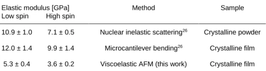
Table 1. Comparison of reported elastic moduli of 1.
Elastic modulus [GPa] Low spin High spin
Method Sample
10.9 ± 1.0 7.1 ± 0.5 Nuclear inelastic scattering26 Crystalline powder
12.0 ± 1.4 9.9 ± 1.4 Microcantilever bending26 Crystalline film
7
Figure 2d shows the temperature dependence of the energy dissipation in 1. Remarkably,
increasing dissipation can be depicted near the spin transition temperature (ca. 338 K). As such,
the results in Figure 2d are indicative of significant internal frictions during the spin transition
and a more viscous HS phase.
A closer inspection of the storage modulus maps at 333 and 338 K in Figure 2a recorded in the
course of the spin transition reveals a LS/HS phase separation – reminiscent of nucleation and
growth phenomena – taking place next to film imperfections (i.e. cracks, crevices or holes).
Driven by the aim to better understand the physical mechanism causing this observation, we
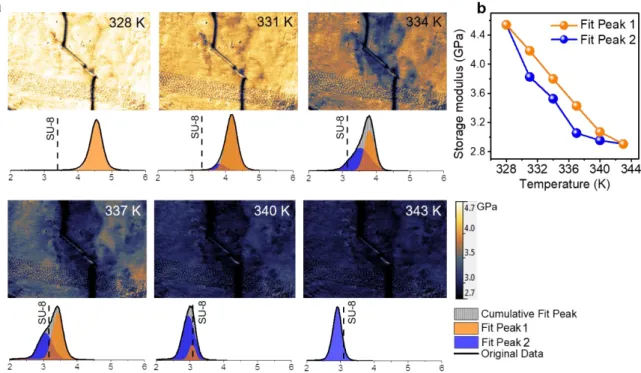
performed a more careful analysis in a small area around a crack. Figure 3a depicts the storage
modulus maps acquired by 3 K steps between 328 and 343 K with a resolution of 7 nm/pixel.
The histograms extracted from the maps of moduli clearly reveal the coexistence of two phases.
At 331 K, one may notice the appearance of a second peak that monotonously grows through
the phase transition. At the same time, the first peak monotonously shrinks and disappears
around 340 K. (This observation was repeatedly made on the same area for more than five
heating-cooling cycles). At first sight, this behavior seems to be similar to the mechanism seen
in macroscopic crystals of 1, where the spin-state switching within the thermal hysteresis region
occurs via a nucleation and growth process.[29] In our case, however, the examination of the
cooling cycle (Figure 2a) does not show any sign of LS phase nucleation. In particular, at 333
K the area around the crack is still in the HS state. We can thus conclude that the formation of these HS “puddles” around the crack does not denote a nucleation process; instead, it
corresponds to a lowering of the spin transition temperature. This is particularly clear in Figure
3b, which displays the temperature dependence of the two elastic moduli peaks: the transition
curve corresponding to the surface area near the crack (denoted ‘Peak 2’) is downshifted by
about 3 K. Interestingly, this shift is approximately of the same order of magnitude – with
opposite sign – as the variation of the spin transition temperature with decreasing film thickness.
8
LS state is progressively stabilized due to its lower surface/interface energy and stress.[19] We
can thus suggest that cracks relieve the surface stress effects and thus restore the HS state in the
film by a strain relaxation mechanism. This stabilization appears efficient up to the micrometer
range around the crack, suggesting that lithographic patterning of the films should lead to a
modulation of their spin transition temperature.
Figure 3. (a) Storage modulus maps around a film defect acquired between 328 and 343 K.
Histograms of the modulus maps (corresponding to the complete scan area) show the co-existence of two zones, characterized by different SCO behaviors. Scan size is 5 × 3.5 μm2. (b)
Temperature dependence of the fitted storage modulus peaks.
The present AFM experiments provide also crucial information for understanding the nature of
the phase transition in the films of 1. It is well known that the large transformation strain, which
accompanies the SCO, may lead to the emergence of discontinuous (first-order) phase
transitions.[42-44] Indeed, in high-quality single crystals of 1, using far-field optical microscopy,
we have repeatedly observed a heterogeneous nucleation, followed by the formation of a fast
moving HS/LS phase boundary, leading to a discontinuity at the transition.[29] Yet, an important
aspect of this transition has escaped our attention. As shown in Figure 4, the discontinuity
9
change their spin state in a rather gradual and spatially homogenous manner before as well as
after the discontinuity. In other words, the SCO in single crystals of 1 is of first order, though
it is certainly very close to the crossover regime.
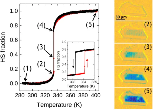
Figure 4. Optical microscopy study of a single crystal of 1 across the spin transition. (Left)
Temperature dependence of the HS fraction in a crystal obtained from the spatially averaged optical transmission at λ = 543 nm during one heating-cooling cycle (2 K/min). The inset shows a magnified version of the thermal hysteresis loop. (Right) Selected optical microscopy snapshots of the crystal at different stages of the transition in the heating mode: (1) nHS = 0, (2)
nHS = 0.17, (3) nHS = 0.35, (4) nHS = 0.76 and (5) nHS = 1. Blue and dark yellow (artificial) colors
indicate the HS and LS phases, respectively.
At first sight, the spin transition curve of the thin film of 1, obtained by far-field optical
microscopy (Figure 2b), is reminiscent to that of the bulk crystal (Figure 4). In particular, a
thermal hysteresis loop of ca. 0.5 K width is reproducibly observed for the films (see ref. 19 for
more details), which is a mark of a first-order transition. On the other hand, no discontinuity
can be discerned in the case of the films. However, the films consist of a large number of tiny
crystals (of ca. 50 nm mean size)[30] with a distribution of the transition temperatures, which
can mask the discontinuity. The high-resolution AFM images across the phase transition in
Figure 2 and 3 allow us to reduce this distribution effect and reveal that the transition in the
280 300 320 340 360 380 400
0.0
0.2
0.4
0.6
0.8
1.0
HS
f
ra
c
ti
o
n
Temperature (K)
333 334 335 0.0 0.2 0.4 0.6 0.8 1.0 H S fra ct io n Temperature (K)(1)
(2)
(3)
(4)
(5)
(2)
(3)
(4)
(5)
30 µm
10
films is indeed not discontinuous anymore. Instead, within the resolution of our measurements,
one can observe a spatially homogenous SCO, which occurs in a continuous manner. We can
thus suggest that the film stress and/or defects alter the intrinsically first-order transition to
become a gradual spin crossover. Finally, it is worth noting that no sign of nucleation and
growth phenomena – indicative of transmission of cooperative interactions through the grain
boundaries – were detected in the AFM images, which is in line with the proposed nature of the
SCO in the films.
In conclusion, we have presented a spatially resolved investigation of the spin transition in
[Fe(HB(tz)3)2] thin films through the quantitative mapping of their viscoelastic properties by
AFM. This approach enabled us to detect – in a reproducible and non-invasive manner – a ca.
30 % decrease of the elastic modulus when going from the LS to the HS state. As it was
demonstrated in several recent reports, the spatial resolution of this technique can reach the
1-10 nm range for various samples,[45-46] which opens up a unique possibility to assess mechanical
properties of SCO materials at the nanoscale, with particular relevance to their possible use in
nanoscale actuator devices.[26,33] The ability of AFM to provide spatially resolved information
on local SCO behaviors allowed us to evidence a very homogenous phase transformation in the
films, except for the vicinity of film defects, which were shown to stabilize the HS state in the
form of sub-micrometric puddles. This phenomenon, ascribed to strain relaxation, is important
when considering the use of these films for sensing and imaging purposes and suggests that
strain engineering should allow for tuning the local and/or global spin transition temperature in
thin films. The nature of the spin transition in the films was also discussed in light of these
results, which allowed us to conclude that the bulk, first-order transition becomes a continuous
crossover in the nanocrystalline films. It would be interesting to modulate the stress state of the
films between tensile and compressive (e.g. by epitaxy) and observe by AFM the concomitant
variation of their spin transition properties. Another interesting perspective consists of the
11
heterogeneous systems, strain coupling plays often an important role,[47-48] but the
corresponding microscopic mechanisms remain difficult to visualize by other methods.
Supporting Information
Supporting Information is available from the Wiley Online Library or from the author.
Acknowledgements
The PhD grants of ACB and MPB were financed by the Occitanie Région and the Federal University of Toulouse. We are indebted to Rafael Barbatini and Roger Proksch (Asylum Research) for their kind help in the analysis of the experimental data.
Received: ((will be filled in by the editorial staff)) Revised: ((will be filled in by the editorial staff)) Published online: ((will be filled in by the editorial staff))
References
[1] Spin Crossover in Transition Metal Compounds I-III, (Eds: P. Gütlich, H. A.
Goodwin), Springer, Berlin Heidelberg 2004.
[2] Spin-Crossover Materials: Properties and Applications, (Eds: M. A. Halcrow), John
Wiley & Sons, Oxford, UK 2013.
[3] Spin Crossover Phenomenon, (Eds: A. Bousseksou), C. R. Chimie 2018, 21, pp. 1055–
1300.
[4] A. Bousseksou, G. Molnár, L. Salmon, W. Nicolazzi, Chem. Soc. Rev. 2011, 40, 3313.
[5] K. S. Kumar, M. Ruben, Coord. Chem. Rev. 2017, 346, 176.
[6] G. Molnár, S. Rat, L. Salmon, W. Nicolazzi, A. Bousseksou, Adv. Mater. 2018, 30,
1703862.
[7] G. Félix, W. Nicolazzi, L. Salmon, G. Molnár, M. Perrier, G. Maurin, J. Larionova, J.
Long, Y. Guari, A. Bousseksou, Phys. Rev. Lett. 2013, 110, 235701.
[8] A. Slimani, K. Boukheddaden, K. Yamashita, Phys. Rev. B 2014, 89, 214109.
[9] D. Chiruta, J. Linares, S. Miyashita, K. Boukheddaden, J. Appl. Phys. 2014, 115,
12
[10] G. Félix, W. Nicolazzi, M. Mikolasek, G. Molnár, A. Bousseksou, Phys. Chem. Chem.
Phys. 2014, 16, 7358.
[11] M. Mikolasek, W. Nicolazzi, F. Terki, G. Molnár, A. Bousseksou, Phys. Chem. Chem.
Phys. 2017, 19, 12276.
[12] K. Bairagi, O. Iasco, A. Bellec, A. Kartsev, D. Li, J. Lagoute, C. Chacon, Y. Girard, S.
Rousset, F. Miserque, Y. J. Dappe, A. Smogunov, C. Barreteau, M.-L. Boillot, T. Mallah, V.
Repain, Nat. Commun. 2016, 7, 12212.
[13] T. G. Gopakumar, M. Bernien, H. Naggert, F. Mationo, C. Hermanns, A. Bannwarth,
S. Mühlenberend, A. Krüger, D. Krüger, F. Nickel, W. Walter, R. Berndt, W. Kuch, F.
Tuczek, Chem. Eur. J. 2013, 19, 15702.
[14] C. R. Gros, M. K. Peprah, B. D. Hosterman, T. V. Brinzari, P. A. Quintero, M.
Sendova, M. W. Meisel, D. R. Talham, J. Am. Chem. Soc. 2014, 136, 9846.
[15] D. M. Pajerowski, J. E. Gardner, F. A. Frye, M. J. Andrus, M.F. Dumont, E. S.
Knowles, M. W. Meisel, D. R. Talham, Chem. Mater. 2011, 23, 3045.
[16] A. Akou, C. Bartual-Murgui, K. Abdul-Kader, M. Lopes, G. Molnár, C. Thibault, C.
Vieu, L. Salmon, A. Bousseksou, Dalton Trans. 2013, 42, 16021.
[17] L. Kipgen, M. Bernien, S. Ossinger, F. Nickel, A. J. Britton, L. M. Arruda, H.
Naggert, C. Luo, C. Lotze, H. Ryll, F. Radu, E. Schierle, E. Weschke, F. Tuczek, W. Kuch,
Nat. Commun. 2018, 8, 2984.
[18] V. Rubio-Gimenez, C. Bartual-Murgui, M. Galbiati, A. Nunez-Lopez, J. Castells-Gil,
B. Quinard, P. Seneor, E. Otero, P. Ohresser, A. Cantarero, E. Coronado, J. A. Real, R.
Mattana, S. Tatay, C. Marti-Gastaldo, Chem. Sci. 2019, 10, 4038.
[19] V. Shalabaeva, M. Mikolasek, M. D. Manrique-Juarez, A. C. Bas, S. Rat, L. Salmon,
13
[20] C. W. Bark, P. Sharma, Y. Wang, S. H. Baek, S. Lee, S. Ryu, C. M. Folkman, T. R.
Paudel, A. Kumar, S. V. Kalinin, A. Sokolov, E. Y. Tsymbal, M. S. Rzchowski, A.
Gruverman, C. B. Eom, Nano Lett. 2012, 12, 1765.
[21] C. Ko, Z. Yang, S. Ramanathan, ACS Appl. Mater. Interfaces 2011, 3, 3396.
[22] M. Lopes, C. M. Quintero, E. M. Hernández, V. Velazquez, C. Bartual-Murgui, W.
Nicolazzi, L. Salmon, G. Molnár, A. Bousseksou, Nanoscale 2013, 5, 7762.
[23] A. Tselev, E. Strelcov, I. A. Luk’yanchuk, J. D. Budai, J. Z. Tischler, I. N. Ivanov, K.
Jones, R. Proksch, S. V. Kalinin, A. Kolmakov, Nano Lett. 2010, 10, 2003.
[24] S. Schreiber, M. Savla, D. V. Pelekhov, D. F. Iscru, C. Selcu, P. C. Hammel, G.
Agarwal, Small 2008, 4, 270.
[25] E. M. Hernández, C. M. Quintero, O. Kraieva, C. Thibault, C. Bergaud, L. Salmon, G.
Molnár, A. Bousseksou, Adv. Mater. 2014, 26, 2889.
[26] M. Mikolasek, M. D. Manrique-Juarez, H. J. Shepherd, K. Ridier, S. Rat, V.
Shalabaeva, A.-C. Bas, I. E. Collings, F. Mathieu, J. Cacheux, T. Leichle, L. Nicu, W.
Nicolazzi, L. Salmon, G. Molnár, A. Bousseksou, J. Am. Chem. Soc. 2018, 140, 8970.
[27] S. Trofimenko, J. Am. Chem. Soc. 1967, 89, 3170.
[28] S. Rat, K. Ridier, L. Vendier, G. Molnár, L. Salmon, A. Bousseksou, CrystEngComm
2017, 19, 3271.
[29] K. Ridier, S. Rat, H. J. Shepherd, L. Salmon, W. Nicolazzi, G. Molnár, A.
Bousseksou, Phys. Rev. B 2017, 96, 134106.
[30] V. Shalabaeva, S. Rat, M. D. Manrique-Juarez, A.-C. Bas, L. Vendier, L. Salmon, G.
Molnár, A. Bousseksou, J. Mater. Chem. C 2017, 5, 4419.
[31] A.-C. Bas, V. Shalabaeva, X. Thompson, L. Vendier, L. Salmon, L. Routaboul, G.
Molnár, A. Bousseksou, C. R. Chimie 2019, 22, 525.
[32] K. Ridier, A.-C. Bas, V. Shalabaeva, W. Nicolazzi, L. Salmon, G. Molnár, A.
14
[33] M. D. Manrique-Juarez, F. Mathieu, V. Shalabaeva, J. Cacheux, S. Rat, L. Nicu, T.
Leïchlé, L. Salmon, G. Molnár, A. Bousseksou, Angew. Chemie Int. Ed. 2017, 121, 8074.
[34] V. Shalabaeva, K. Ridier, S. Rat, M. D. Manrique-Juarez, L. Salmon, I. Séguy, A.
Rotaru, G. Molnár, A. Bousseksou, Appl. Phys. Lett. 2018, 112, 013301.
[35] L. Poggini, M. Gonidec, J. H. Gonzalez-Estefan, G. Pecastaings, B. Gobaut, P. Rosa,
Adv. El. Mater. 2018, 4, 1800204.
[36] M. Kocun, A. Labuda, W. Meinhold, I. Revenko, R. Proksch, ACS Nano 2017, 11,
10097.
[37] A. Labuda, M. Kocuń, W. Meinhold, D. Walters, R. Proksch, Beilstein J.
Nanotechnol. 2016, 7, 970.
[38] R. Garcia, R. Proksch, Eur. Polym. J. 2013, 49, 1897.
[39] J. Liu, D. S. Grierson, N. Moldovan, J. Notbohm, S. Li, P. Jaroenapibal, S. D.
O'Connor, A. V. Sumant, N. Neelakantan, J. A. Carlisle, K. T. Turner, R. W. Carpick, Small
2010, 6, 1140.
[40] S. Chung, S. Park. J. Mech. Sci. Technol. 2013, 27, 2701.
[41] D. Passeri, M. Rossi, E. Tamburri, M. L. Terranova, Anal. Bional. Chem. 2013, 405,
1463.
[42] H. Spiering, K. Boukheddaden, J. Linares, F. Varret, Phys. Rev. B 2004, 70, 184106.
[43] K. Ridier, G. Molnár, L. Salmon, W. Nicolazzi, A. Bousseksou, Solid State Sci. 2017,
74, A1.
[44] F. Varret, C. Chong, A. Slimani, D. Garrot, Y. Garcia, A. D. Naik, in Spin-Crossover
Materials: Properties and Applications, (Ed: M. A. Halcrow), John Wiley & Sons, Oxford, UK 2013, pp. 425–441.
[45] S. Benaglia, V. G. Gisbert, A. P. Perrino, C. A. Amo, R. Garcia, Nat. Protocols, 2018,
13, 2890.
15
[47] Y.-S. Koo, J. R. Galán-Mascarós, Adv. Mater. 2014, 26, 6785.
[48] S. Rat, M. Piedrahita-Bello, L. Salmon, G. Molnár, P. Demont, A. Bousseksou, Adv.