E-BROIDERY: AN INFRASTRUCTURE FOR WASHABLE COMPUTING
by
E. Rehmi Post
B.S., Physics
University of Massachusetts, Amherst
May 1996
Submitted to the Program in Media Arts and Sciences, School of Architecture and Planning, in partial fulfillment of the requirements for the degree of Master of Science in Media Arts and Sciences
at the Massachusetts Institute of Technology February 1999
MASSACHUSETTS IN TITUT
@1998
Massachusetts Institute of Technology. All rights reserved. OF TECHNOLOGYJUL
2 0
LIBRARIES
Author <
E. Rehmi Post Department of Media Arts and Sciences October 9, 1998
Certified by
Neil Gershenfeld vs Arciate Profssor of Media Arts and Sciences
MIT Media Lab
Accepted byStephen A. Benton Professor of Media Arts and Sciences Chair, Departmental Committee on Graduate Students Program in Media Arts and Sciences
Acknowledgments
I must first acknowledge the greatest debt to my parents, Edward and Zehra Post, without whom I would not be, and to my brother Burton for sharing that debt with me.
Along the way, there were many who would always take time to show me their favorite places to scratch the world I already knew to reveal wondrous new things. Those whose names I can remember at the moment include Beatrice Domanski, Joy Odom, Charles Rieger, Mark Weiser, Randy Trigg, Charles Adler, Don Hopkins, Michelle McElvany, Mike Gallaher, Sarah Kaye, Margaret Wasserman, Steve Wadlow, H. Shrikumar, Mark Tuominen, Eugene Golowich, Andy Barto, Rob Gramer, and Sam Holland.
At the Media Lab, I've been lucky to have a wise, talented, and almost hyperactively enthusiatic advisor in the person of Neil Gershenfeld, whose unfailing support for my wild ideas has not gone unnoticed. I've been fortunate to work with many good and genuine people here, including Joe Paradiso, Bernd Schoner, Matt Reynolds, Lenny Foner, Thad Starner, Brad Rhodes, Babak Nivi, Kwin Kramer, Yael Maguire, and Joe Pompei. It's also an honor to have been an Interval Research Fellow during my first two years at the Media Lab.
I am also deeply grateful to have worked with several motivated and talented people while building the Musical MIDI Jacket, including Josh Smith, Josh Strickon, and Emily Cooper, and especially Maggie Orth, who sparked our imaginations by testing her wedding dress with an ohmmeter to find it was conductive, while Tod Machover supported our work.
Paul Rosenstrach, Rick Tumminelli, and John LeBlanc of the Charles Stark Draper Labs all cared enough about this work to see it through to the implementation of a flexible multichip fabric readout
module.
Finally, I dedicate this work to Jenny Gutbezahl, whose unfailing love and caustic wit have some-how conspired to keep me true.
E-BROIDERY: AN INFRASTRUCTURE FOR WASHABLE COMPUTING
E. Rehmi Post
Submitted to the Program in Media Arts and Sciences, School of Architecture and Planning, on October 9th, 1998, in partial fulfillment of the requirements for the degree of Master of Science in
Media Arts and Sciences
Abstract
Wash-and-wear multilayer electronic circuitry can be constructed on fabric substrates, using conduc-tive textiles and suitably packaged components. Fabrics are perhaps the first composite materials engineered by humanity; their evolution led to the development of the Jacquard loom, which itself led to the development of the modern computer. The development of fabric circuitry is a compelling closure of the cycle that points to a new class of textiles which interact with their users and their environments, while retaining the properties that made them the first ubiquitous "smart material". Fabrics are in several respects superior to existing flexible substrates in terms of their durability, con-formability, and breathability. The present work adopts a modular approach to circuit fabrication, from which follow circuit design techniques and component packages optimized for use in fabric-based circuitry, flexible all-fabric interconnects, and multilayer circuits. While maintaining close compati-bility with existing components, tools, and techniques, the present work demonstrates all steps of a process to create multilayer printed circuits on fabric substrates using conductive textiles.
Advisor: Neil Gershenfeld
E-BROIDERY: AN INFRASTRUCTURE FOR WASHABLE COMPUTING
Thesis Readers
Advisor
Neil Gershenfeld Associate Professor of Media Arts and Sciences Director, Physics and Media Group Thesis Supervisor
Professo: Director, Academic Head, MIT Progran
Alex Pentland r of Media Arts and Sciences Vision and Modelling Group i in Media Arts and Sciences
Reader
r-
PfsJoseph JacobsonAssistant Professor of Media Arts and Sciences Director, Micromedia group Reader
Contents
1 Introduction 9
1.1 How to make washable circuitry. . . . . 10
1.2 A wash-and-wear digital infrastructure.. . . . . . . . 11
1.3 Previous Work in Conductive Textiles.. . . . . . . . . 12
1.4 Case study: The Wearable MIDI Jacket . . . . 13
2 Context and Implementation of Work 17 2.1 A bstraction . . . . . . 18
2.2 Implementation Goals... . . . . . . . .. 19
3 Fabrication techniques 21 3.1 Flexible circuit substrates . . . . 22
3.2 Flexible multi-chip modules . . . . 23
3.3 Electrically active textiles . . . . 24
3.3.1 Metallic silk organza . . . . 24
3.3.2 Conductive yarn . . . . 26
3.4 Other interconnection strategies . . . . 26
3.4.1 G ripper snaps . . . . 26
3.5 Component packaging . . . . 27
3.5.1 The case for round packages . . . . 27
3.6 The Plastic Threaded Chip Carrier . . . . 29
3.6.1 Protoyping the PTCC . . . . 29
3.6.2 Spot w elding . . . . 31
3.6.3 Weld evaluation . . . . 33
3.7 E-broidered circuitry . . . . 34
3.7.1 E-broidered composites . . . . 38
3.8 Implementation of the MIDI Jacket keypad . . . . 38
3.9 Multilayer circuit construction . . . . 38
4 Future work 41
A MIDI Jacket keypad implementation 45
Chapter 1
Introduction
One of the few constants in modern society is that everybody wears clothing. Clothing serves many functions: it provides us with a sense of the wearer's identity; it affords protection from the environ-ment; and it gives the wearer pockets or other convenient places to store small objects.
All of these functions are also served by wearable computing [SMR+96] in a digital analog. If the user inhabits an information-rich environment a wearable computer can provide others with chosen details of the user's identity and preferences. It can protect the user by mediating his/her experience and refining a torrent of raw data into a salient stream of information, linked to the immediate physical and informational context. And it provides a place to store informational objects the user might wish to use later.
Of course, wearable computing has a number of precedents. Since the beginning of the digital era computers have followed a trend of becoming smaller, faster, and more personalized. In the early 1980's the personal computer revolution began to put computers on every desk, while cellular telephones and pagers changed personal communications. In the late 1990's, personal, miniaturized digital systems have become increasingly important in many people's everyday lives. With the privatization of the Internet and the birth of the World Wide Web, "being connected" has emerged as a popular concern. But the electronic gear that makes this information revolution possible still takes an awkward form. It's not truly wearable except in the sense that it will fit in your pocket or strap onto your body. What we need is a way to integrate technology directly into clothing.
The goal of this work is to make electronic circuitry disappear into clothing, by replacing circuit boards with fabric circuitry and by using component packages designed for use in fabric circuits. Several of the reasons to do this are outlined below, all stemming from the desire to make e-garments with integrity. An e-garment's integrity depends on its ability to look, feel, wash, and wear as well as
CHAPTER 1. INTRODUCTION
ordinary clothing does.
Circuit boards do not look or feel good when they become part of your clothing, nor do they wash well. We might address this by making the circuit board smaller and removable, by redesigning it to use the same components in smaller packages and by using conductive fasteners to connect boards and garments (so that boards can be removed when a garment goes into the wash.) The trouble is, this approach doesn't scale well: the whole circuit board still has to be assembled and tested, and somehow connected to the fabric. Worst of all, there are still several layers of packaging between the silicon and the silk.
All of this points to a better way of doing things. Rather than choosing packages to increase component density on a circuit board, one might instead choose packages to do the same thing in a fabric circuit. One might also choose to package components so they can be washed without com-promising their electrical connection to the garment and to other components. Finally, the interface between components and circuitry must withstand the flexing and stretching that clothing is prone to experience.
1.1
How to make washable circuitry
Commonly, printed circuit boards (PCBs) have two or more layers of printed conductive traces which interconnect components soldered onto exposed portions of the outermost layers. This method of circuit fabrication is pervasive, so it would be good for any technique we develop be compatible with exisiting printed circuit layout tools. Consequently, we adopt a modular approach in which components and printed circuit strata are produced separately and then joined in standardized ways to produce circuits of arbitrary complexity.
The first part of this work is to identify good materials for use in fabric circuitry. This involves a tradeoff between electrical mechanical properties: we want to use a thread that is reasonably con-ductive but that can be sewn at high speed in commercial embroidery processes. Such an approach builds on prior art in textile manufacturing to develop a composite yarn that balances these properties and is also washable. For the purposes of this work, we consider dry-cleaning as the target washing process, and exposure to water, alcohols, and sweat as an everyday occurrence.
The second part of this work shows how to design packages optimized for use in fabric circuitry. The focus of this effort is the design of the "Plastic Threaded Chip Carrier" (PTCC), a package that bears a resemblance to the Plastic Leadless Chip Carrier (PLCC). The PLCC is a well-known surface-mount IC package style, designed to be soldered onto printed copper circuit traces on a rigid or semi-rigid circuit board. Conversely, the PTCC is designed to be stitched or woven into a fabric circuit, and for this purpose has long, flexible conducting leads.
1.2. A WASH-AND-WEAR DIGITAL INFRASTRUCTURE
The third part of this work is to develop a way to sew multi-layer circuitry into fabric. Even if we can sew a circuit, its complexity will be limited if it is restricted to two dimensions. This part of the present work builds on existing techniques on embroidery that achieve particular effects of texture and appearance.
The goal is to demonstrate the feasability of wash-and-wear articles that integrally include digital circuitry, to provide data on the lifetime of such circuitry, and to describe the particulars of the relevant fabrication methods. Ultimately we would like to demonstrate that textile-based circuitry compares favorably to ordinary printed circuit boards in terms of its complexity and reliability. It must also be more durable than printed circuit boards are when exposed to the mechanical, thermal, and other environmental stresses that clothing and wearable items normally experience.
Beyond the applications to clothing, this work will make possible the construction of circuits with a high degree of flexibility including user interfaces that conform to irregularly shaped surfaces.
1.2
A wash-and-wear digital infrastructure
Imagine wearing your computer all the time. Your interactions with it would not require a rigid, structured form but would instead incorporate your motions, your gestures, and aspects of your affect and environment as a context for the interaction [SMR+96].
Giving the computer this detailed level of awareness of its user is akin to giving the computer a "skin" in the real world. Think of how we interact through our interfacial layer with the world around us. In one sense, we are proposing to merge the computer's skin with our clothing. This idea has a precedent in the Al community, particularly in the work of Rodney Brooks, who suggests that behavior that seems to be "intelligent" evolves as a response to sensory presence in a physical environment.
Merging computing and clothing is in some ways also a departure from the traditional view of the cyborg: a half-human, half-cybernetic organism where biological and digital systems combine in synergy. These "borgs" often have an imposing presence, if only because they appear to live within a carapace of impact-resistant plastic, heavy-duty wiring, and obvious bulges of siliconic ganglia. This is really a difference in fashion and appearance, not in motivation. What we propose here is a way to unobtrusively integrate digital systems into clothing.
Portable phones and pagers are two kinds of personal digital systems that have benefited from intense efforts at miniaturization. Due to the economies of scale, the cost of manufacturing these devices has fallen to the point where it is "in the noise" compared to the cost of maintaining the infrastructure necessary for their operation. By increasing the potential user base to anyone who wears clothes, the cost of devices integrated into clothing could be lowered even farther.
CHAPTER 1. INTRODUCTION
One might imagine a wearable computer composed of several parts, each integrated into a separate article of clothing. For example, it has been proposed that shoes are a good place to put computing equipment, because of the space available in the shoe itself as well as the power that potentially can be extracted from the human gait. The shoe is also a good location for a system to transmit and receive data [Zim95] and power [PRPG97] through the body.
1.3
Previous Work in Conductive Textiles
The state of the art in textile circuitry seems to be largely unpublished and proprietary. At the time of this writing, I have not been able to find any prior art relating to the construction of actual circuitry in fabric using off-the-shelf electronic components and ordinary fabric. While a great deal of work has been done in the field of electrically active textile technology, it appears that almost none at all has been done in the construction of active electronic circuits on or in fabric.
An inspirational exception to this was an experiment conducted by Michael Hawley at the Media Lab, which (among other things) sought to impart electronic circuitry into fabric. This path was abandoned because the appropriate materials and techniques were not identified. The development of these methods is informed by both the properties of the materials used and by the capabilities of printed circuit board fabrication technology.
There are, of course, many related threads of ongoing work. A survey of the U.S. Patent literature reveals that most workers are focusing on the development of synthetic conductors compatible with existing textile production processes. For example [GKK89], there are certain conductive polymers which retain a comparatively high conductivity (approx. 1Q .m-1) after being spun into threads
which have the weight, strength, and appearance of ordinary nylon thread.
Another knot of work focuses on the production of conductive materials and processes for printing them onto fabric [GGJ92]. Workers in this area cite the possibility of "tagging" apparel by printing tuned LC circuits directly onto the fabric, rather than by attaching separate, removable anti-theft tags. This problem is also addressed by workers who seek to embed magnetostrictive tags directly into clothing but this is not directly related to constructing circuitry directly in clothing.
Still others are working on embedding photonic conductors (optical fibers) into clothing to build architectures for sensing and data distribution. The sensate liner [LEB+97] lies in this strand, in which a woven fiber optic matrix is used to sense disruptions of the weave (by measuring optical continuity) and to perform spectrographic analysis of the materials present at intrusions. Such analysis can be used to determine the type and severity of wounds suffered by the wearer of the liner. This line of work is promising because of the variety of fiber optic sensors that can be made, but their largest drawbacks arise from the interface to conventional electronics that are required for signal origination
1.4. CASE STUDY: THE WEARABLE MIDI JACKET
and processing.
1.4
Case
study: The Wearable MIDI Jacket
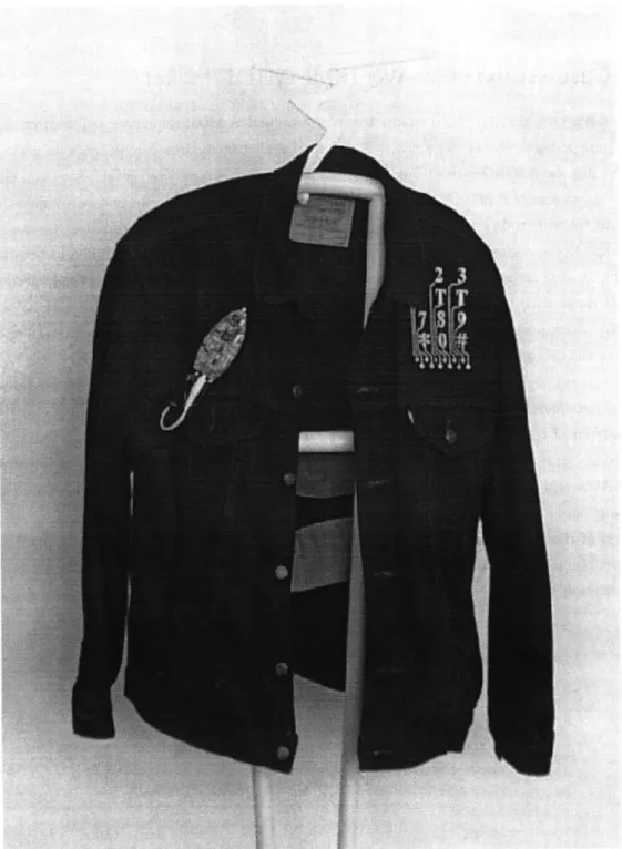
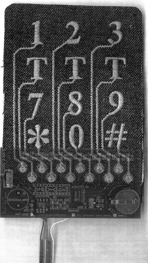
This wearable system integrates a conductive fabric keypad, a MIDI sequencer/synthesizer, and loud-speakers into a denim jacket. The jacket demonstrates that keyboards can be made in a single layer of fabric using capacitive sensing [Bax97], where an array of embroidered or silk-screened electrodes make up the points of contact. A finger's contact with an electrode can be sensed by measuring the increase in the electrode's total capacitance. It is worth mentioning that this can be done with a single bidirectional digital I/O pin per electrode, and a leakage resistor sewn in highly resistive yarn. Capacitive sensing arrays might also be used to tell how well a piece of clothing fits the wearer, because the signal varies with pressure.
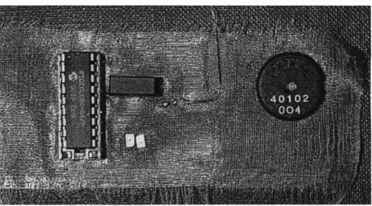
The keypad shown here has been mass-produced using ordinary embroidery techniques and mildly conductive thread. The result is a keypad that is flexible, durable, and responsive to touch. A printed circuit board supports the components necessary to do capacitive sensing and output keypress events as a serial data stream. The circuit board makes contact with the electrodes at the circular pads only at the bottom of the electrode pattern. In a test application, 50 denim jackets were embroidered in this pattern. Some of these jackets are equipped with miniature MIDI synthesizers controlled by the keypad. Although no user studies have been conducted, the responsiveness of the keyboard to touch and timing were found by several users to be excellent.
A view of the component side of the circuit board has been superimposed to show its extent and its connections to the fabric. A flexible circuit board can be substituted for the rigid one used in this implementation. The work which follows describes how to do away with the circuit board entirely.
14 CHAPTER 1. INTRODUCTION
1.4. CASE STUDY: THE WEARABLE MIDI JACKET
Figure 1.2: Composite image of denim keypad and readout circuit board.
ljok Moofth, -,. I ---
Chapter 2
Context and Implementation of
Work
Electrical circuits are typically assembled by soldering active and passive electrical components onto solid boards. The components receive power and exchange signals by means of a network of conductive metal traces patterned in multiple layers on the board.
This approach to circuit fabrication is nearly universal, but it limits the form taken by electronic devices. Rigid boards must be housed within rigid cases, so the notion of electronics being packaged in "boxes" is ubiquitous and alternatives are difficult to imagine.
As the miniaturization of circuits continues, and as the suite of electronically useful materials expands, alternatives to the tradition of rigid housings and circuit boards will become increasingly important. At the time of this writing, most consumer electronics are housed in so-called "biomorphic" packages designed to have smooth curves rather than hard edges.
Current work into user interface design attempts to bring electronic sensing and display circuitry into more intimate contact with users. Interaction with digital objects is likely to become as common as interaction with objects that are not informationally enhanced. In this way, the user is spared the need to deliberately "operate" an external system.
The range of useful tasks amenable to digital mediation is likewise increased. In this vision, environment and location monitoring, information storage, processing and mediation, and short- or long-range digital communication may all be effected without effort by the user or proximity to external electronic devices.
CHAPTER 2. CONTEXT AND IMPLEMENTATION OF WORK
2.1
Abstraction
Most integrated circuits and discrete components are available in standard packages meant to attach to printed circuit boards. These components are usually soldered into place, although conductive adhesives have recently shown promise as alternatives to solder.
To be compatible with current components, we would like to preserve certain properties of printed circuit boards when building circuits in fabric, as well as drawing upon existing knowledge in flexible circuit fabrication.
" Electrical properties: The versatility of printed circuits is due in part to their applicability over a broad range of frequencies, from zero to several gigahertz. At low frequencies, the circuit designer is free to consider the printed traces to be nearly ideal conductors, much like the lines connecting components in a circuit diagram. At higher frequencies, however, the traces themselves become
circuit elements, as their feature size becomes similar to the length of the signals they carry. " Mechanical properties: Printed circuits often comprise copper bonded to some substrate, such as
a fiberglass/epoxy hybrid. The substrate is strong, flexible, and electrically well- characterized. It has good dimensional stability, and damps mechanical vibration. There are more exotic substrates, optimized for flexibility (Kapton, for example) or connection density (multi-chip modules).
" Component packaging and bonding: The mechanical properties of a printed circuit also influence the ways in which components can be connected to it. The best way to connect integrated circuits (ICs) is to wirebond them directly to one another or to an interconnecting substrate. This can be an exacting process, so most components are instead mounted in packages of standard shape, size, and pin arrangement. These packages trade off larger connections and more tolerance for error against connection density and parasitic electrical characteristics. Recently, the Ball Grid Array has been promoted as a high-density connection scheme, in which an array of pads on an IC's surface connect directly to a printed circuit through small metal balls and an optional protective layer.
It is alluring to think of woven circuitry, where components are formed by the junctions of individual threads with different material properties. As a modest and practicable first step toward that end, we propose to address the properties of substrates, interconnects, and component packages in the context of textile-based circuit fabrication.
Interconnections must be both mechanically and electrically stable, at the interface between com-ponent and textile, and along the run of the interconnecting textile. This requirement affects the
2.2. IMPLEMENTATION GOALS
bonding strategy, the component packaging, and the choice of material. We will explore each of these areas in turn, by designing and evaluating
" methods for component bonding,
* packages and lead patterns optimized for use with textiles, and
" composite materials designed with strength, conductivity, and washability in mind.
2.2
Implementation Goals
Rather than confronting the problem of synthesizing conductive polymers, one may instead relax the requirement of highly conductive interconnections, and instead use circuit elements that have low power requirements and high input impedance. This allows one to bootstrap the evolution of fabric circuitry. Such an approach led to the construction of fabric interconnects and sensing arrays in the Wearable MIDI Jacket.
The primary goal is to demonstrate a durable interconnection scheme for components in fabric, replacing printed circuits by stitched circuits. It has already been mentioned that material properties are crucial in this regard. It is also important to consider the patterns in which conductive threads are stitched, because this also strongly determines the electrical properties of the resulting circuitry.
This also points out the possibilities of replacing discrete components such as capacitors, resistors, and inductors by specific combinations of thread and stitch pattern. This can lead to reduced man-ufacturing cost and higher reliability, but it also is a starting point for the discussion of components formed by combinations of different materials.
Another form of stitched component is the sensor. In the case of the wearable MIDI jacket, stitching forms both an interconnect and an array of capacitive sensors, with the distinction arising from differences in contact area and material properties influenced by the stitch pattern. Sensing can also be done by the thread itself, or by the materials which permeate the thread.
The primary circuit placement method is embroidery with conductive thread, or e-broidery. In this case, conductive thread is stitched in patterns defining conductive regions, to produce circuit traces, component connection pads, or sensing surfaces. So far this work has been limited to a single layer of stitching, but it may be possible to build a repertoire of multi-layer embroidery techniques. The simplest test of this would be to embroider a pair of traces where one crosses over the other without direct electrical connection between the two. A more ambitious idea would be to embroider multilayer sensing structures, such as a normally-open electrical switch, where an intermediate layer separates two conducting stitches unless the top conductor is pressed.
CHAPTER 2. CONTEXT AND IMPLEMENTATION OF WORK
The foremost goal of this inquiry has been to generate the tools and processes whereby a designer may construct e-garments that can withstand daily use and dry cleaning. Rather than seeking to supplant conventional packaging and construction of wearable computers, we start instead at the boundary between users and their computers and describe a way of constructing interfaces that have the familiar look and feel of clothing.
In this context, system integration could mean partitioning a digital system across several items of clothing. Part of this is trading functionality against cost. For example, most people have only a few pairs of shoes, a few more pairs of pants, several shirts, and a few outer garments. So it makes sense to put the most expensive parts of a system in the shoes and outer garments, and the least expensive parts in the shirt and pants.
The main body of this work therefore lies in describing new form factors for components destined for use in wash-and-wear fabric circuit substrates, as well as a means of constructing non-trivial circuits on fabric substrates that retain the appearance of ordinary wearable cloth. Component packages are now optimized to interface with printed circuit boards, so we instead optimize them to interface with textile circuitry. Ultimately, we hope this work will lead to an actual packaging standard used by the integrated circuit industry.
Chapter 3
Fabrication techniques
There are several ways to embed electronic circuitry in fabric, depending on the choice of substrate. Some possibilities explored in the course of this work include
* soldering surface-mount components directly onto metallic organza, " bonding components to a substrate using conductive adhesives,
e "stapling" components into a conductive stitched circuit (pressure-forming their leads to grip circuit pads), and
" couching a component's threadframe directly into a circuit (where components are formed with a single conductive thread per pin).
The last possibility is the one explored most fully in the present work, because the others have been ruled out for various reasons.
* Solders used with electronic components are soft alloys of lead (Pb), tin (Sn), and sometimes silver (Ag). Such compounds are not suitable for use in applications in which they could poten-tially be in constant contact with a user's body, because of their toxicity. Worse yet, while it is possible to solder components onto metallic organza and achieve (very) good electrical contact, the mechanical properties of the joint are unsuited to the flexure it will be subjected as an item of apparel.
* Conductive adhesives are better suited to this application than solder, because it is possible to envision adhesives that are non-toxic, highly conductive, higly durable, and moderately flexible to act as a "mechanical impedance match" between a flexible fabric substrate and a rigidly
CHAPTER 3. FABRICATION TECHNIQUES
packaged component. They remain an open possibility and should be the subject of further study.
* Stapled components are an interesting compromise, where a component lead grips a sewn con-ductive trace by being pressed into shape around it. When the substrate flexes, the trace is free to move within the clasp of the formed lead, forming a self-wiping contact at every junction be-tween fabric circuitry and component pins. However, the dimensional rigidity of the component is a poor match for freedom of motion enjoyed by a fabric substrate, and the mismatch is likely to stretch open pins that have been formed into clasps and to accelerate wear and tear of the fabric substrate.
3.1
Flexible circuit substrates
Many methods already exist to fabricate circuits on flexible substrates. Most of these rely on the metallization of a flexible polymer substrate that can withstand the high temperatures of conventional soldering processes. Kapton film, for example, is one of the most commonly used flexible substrates, typically finding applications in cameras (where circuitry must fit intimately into available space in a small package), printers and portable computers (where a large number of connections must cross a hinge or other rotating joint), and non-planar antennas (where the antenna elements must have accurate dimensions yet be shaped to fit on conical forms).
When circuitry is designed for such a substrate, care must be taken to insure that in the final application mechanical stress will not be applied to the component-circuit solder joints. A consequence of this fact is that the parameters of motion of the flexible substrate must be well-understood at the time of design, or rather, that constraints must be imposed on the motion of conventional flexible substrates to ensure that they continue to work over their expected lifetime.
In this respect, conventional flexible substrates are flexible only in regions where components are not attached. Although many such substrates are well-characterised and have electrical properties highly suited to their use in forming electronic interconnects, their mechanical properties still leave something to be desired.
The case against conventional flexible substrates is summed up in the observation that they cannot be (non-destructively) crumpled the way that cloth can be.
3.2. FLEXIBLE MULTI-CHIP MODULES 23 o0pF Th~ ppT , -T; is3J OSC~ICLKI OSC21LK01)T LR R1
3.2
~ ~
lici9oue
~
~
Flxbem
~
R3
textil~~~~
~Te
productsmoinga senspor anl reprthisttstacorlinhs.TefbiainpoesThe major part of thisR redot lmenfrt IC, actv low(when prgamicootrng)Cvsblneneth
titaniumcopperiteonnetins. TRDEn:] todbetcon to elthoes.C68 hr r ou Qci eitr and 16pE cip apaitore .1 Aschematic fo the "fCexisle"w mlinchigue.anisimlrtth
3.2 Flxil muli-hi modules
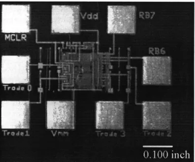
cicuterestin exeptabin kepa tin ule mplicity and fexie oflticrocontrduler.MMaeapeo wInh is sew the hostr 3.2.ahs todue RBs and rsul pins awcollabormo wit fulldupers at3 theal dtalk peraingator 960 bauduce conn, etinsexie foredit dllemo h entsethtmyob embedsi andtineprotigasmalpnie to pedsnosadressrei sahusa to a contring e-tefbroieeicttace powess for thescircuit is suiedlarosth dvloped VmmpinenderaloietiMME/F elcrodes [ar95].cedt
The majeor3 pins tothiscreadotvelyemeadt, justPIC16F8 oicrocnalfarclleyC, diied. reth
Theui uednte fMCMi meae 0.60 inchsimplicit nchoie 0.01 miccothikanller.emisil
bdin orai ofcrature0 obu The cm.nneconsruc thise bydrClng the cttentr compoentas
the Trode/0-3/pinsTh togn be cappitiely areadot uta h rgnlfbi epddd
bendingradiusL of curvtur of n aboth 50C cm.e 1 Toh cognutti MMgh)cnttetcmoet
were thinned to 0.006 inch by mechanical grinding and lapping of the rear face of each component. The components were then placed on a rigid substrate, a Kapton mask (also 0.006 inch thick) with
CHAPTER 3. FABRICATION TECHNIQUES
Figure 3.2: Micrograph of a "flexible" multi-chip module.
windows cut out to accomodate the chips was placed around the chips, and the Ti/Cu interconnect was deposited through a mask. This process extends to multilayer circuitry as well through the use of thin insulating layers. Finally, a protective Kapton cover is glued to the top of the circuit module, the module is removed from the rigid substrate, and a Kapton cover is glued to the bottom of the module, resulting in a completely encapsulated element.
3.3
Electrically active textiles
Many textiles have properties that suggest their use in electronic circuitry. There are all possible com-binations of synthetic and natural fibers, coated or wrapped or spun with metallic fibers or conductive polymer fibers. In this section, some of these materials are identified and described.
3.3.1
Metallic silk organza
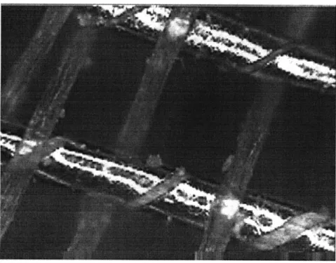
In its primary form, this is a finely woven silk fabric with a thin gold helix wrapped around each thread that runs along the weft of the weave (Figure 3.3.1). Believed to have originated in India, this sort of fabric has been produced for centuries, and appeared in Western fashion as early as the
3.3. ELECTRICALLY ACTIVE TEXTILES
Figure 3.3: Micrograph of metallic organza.
mid-18th century [Har97].
The warp of this fabric consists of parallel silk threads. Through this warp, the weft is woven with a silk thread that has been wrapped in a metal foil helix. This metallic thread is prepared just like cloth-core telephone wire, and is highly conductive. The silk fiber core has a high tensile strength and can withstand high temperatures, allowing the yarn to be sewn or embroidered with industrial machinery. The spacing between these fibers also permits them to be individually addressed, so a strip of this fabric can function like a ribbon cable. If a section of organza is subjected to shear, the cells formed by the weave also shear to form parallelograms, keeping the conductive fibers parallel and separated at all times.
Circuits fabricated on organza only need to be protected from folding contact with themselves, which can be accomplished by coating, supporting or backing the fabric with an insulating layer which can also be cloth. Also, circuits formed in this fashion have many degrees of flexibility (i.e. they can be wadded up), as compared to the single degree of flexibility that conventional substrates can provide.
In the microcontroller circuit shown in Figure 3.4, a PIC16C84 microcontroller and its supporting components are soldered directly onto a patch of metallic organza. This circuit uses the bidirectional
CHAPTER 3. FABRICATION TECHNIQUES
Figure 3.4: A fabric breadboard or "smartkerchief".
I/O
pins on the PIC to control LEDs and to sense touch along the length of the fabric, and uses audible feedback through a piezoelectric speaker to reinforce the sense of interaction. All of the components are soldered directly onto the surface of the metallic organza weave.3.3.2
Conductive yarn
There are also conductive yarns manufactured specifically for producing filters for the processing of fine powders. These yarns have conductive and cloth fibers interspersed throughout. Varying the ratio of the two constituent fibers leads to differences in resistivity. These fibers can be sewn to create conductive traces and resistive elements.
3.4
Other interconnection strategies
3.4.1
Gripper snaps
Gripper snaps make excellent connectors between fabric and electronics. When a two-piece gripper snap is placed on fabric, the first piece has several metallic "teeth" which pierce the substrate and any conductors, making a wiping contact which scrapes off some surface contamination. The second piece is then pressure-formed with the first, cold-welding the teeth into the body of the snap. The
3.5. COMPONENT PACKAGING
snap provides a robust electrical contact that allows subsystems snapped into clothing during use to be removed for washing.
3.5
Component packaging
By and large, integrated circuits with a large number of connections have pins (or other connections) placed on a regularly-spaced square grid. Connections are made to leads around the periphery of a rectangular package or (more densely) to pins or pads on the undersurface of a square package.
As the connection density increases, the leads themselves become shorter and narrower, as does the spacing between them. Of package styles currently in common use, the one with the greatest surface connection density is the ball grid array (BGA).
However, components destined for placement in fabric circuitry do not demand high connection densities, as a consequence of the design principles mentioned above.
3.5.1
The case for round packages
The packaging scheme proposed in the present work creates parts with threads leading out from the component. These threads are then attached to the embroidered circuit substrate by a covering stitch which holds each thread onto the substrate and electrically connects it to a particular sewn conductor. Figure 3.5 illustrates components in square and round packages stitched onto a fabric substrate, while Figure 3.6 shows an actual stitched prototype component couched onto a fabric substrate.
For a given lead spacing at the periphery of a package (s) and a given package diameter (d) or side length (1) the maximum number of threads coming out of each type of package is found to be
nsquare 4(- - 1) (3.1)
S
7rd
nround = - (3.2)
For a given thread spacing around the periphery of the package, it's clear that for a large number of pins the square package will have a smaller diameter than the round package. But if the number of pins is less than 16 (or to be exact, 416 - 4), then the round package is will be a better use of
available space.
The finest practical thread spacing achieved in the present work has been 0.050 inch (1.27 mm), which for 16 leads implies a package diameter of 0.254 inch (6.48 mm). It is practical to expect that a die of about half this width will fit into the package, which gives an upper bound of 10 mm2 of
CHAPTER 3. FABRICATION TECHNIQUES
Steel threads
Steel/Nomex composite threads
Figure 3.5: Square and round packages sewn onto fabric.
3.6. THE PLASTIC THREADED CHIP CARRIER
3.6
The Plastic Threaded Chip Carrier
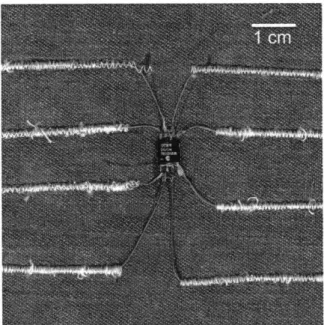
Now we look to the practical aspects of building packages like those that have been described so far. To manufacture threaded packages, we would start with a bare die, add a "threadframe", and connect the near ends of the threadframe to the bondout pads of the die.
Figure 3.7 shows the possible construction of such a component package. Some details have been omitted for clarity, such as the metal base which helps to keep the die substrate at near-uniform temperature and electrical potential across its area.
Connections directly to the die are made in the usual way; fine gold wires are thermocompression-bonded to on one side to the die's gold-plated "bondout pads" and on the other to the stubs of a conventional copper leadframe.
In most packages, the leadframe continues out of the plastic package and is ultimately soldered or cold-welded to external circuitry. But instead of having a solid external leadframe, the plastic threaded chip carrier (PTCC) has flexible, corrosion-resistant threads intended to connect to external circuitry.
In this case, the threads which leave the package are bundles of approximately one hundred con-tinuous steel fibers, each about 5 pm in diameter. These fiber bundles are microspotwelded to the leadframe stubs, and the entire structure is hermetically sealed in a plastic carrier.
3.6.1
Protoyping the PTCC
To test the proposition of a threaded chip carrier, prototypes must be built to evaluate their electrical, mechanical, and sartorial performance.
Since part of the PTCC's assembly process is common to most IC packages, we can test the design principles behind the PTCC without building one completely from scratch. Leaded surface mount (SMT) IC packages already incorporate the die, the leadframe, and bonding wires in a sealed plastic carrier, and their electrical characteristics are well understood.
Prototypes have been built by starting with SMT packages, adding a few components directly to the leads, then microspotwelding steel fiber bundles to the leads. Finally, the threads are arranged in a radial pattern, and the entire assembly is encapsulated in an epoxy resin.
Packages made this way are larger than they need to be, but all of the new design principles involved are represented and open to refinement.
CHAPTER 3. FABRICATION TECHNIQUES
Threadframe (Steel)
Leadframe (Cu)
Bnu
wires (Au)
Bondout pads (Au-plated)
Integrated circuit
3.6. THE PLASTIC THREADED CHIP CARRIER
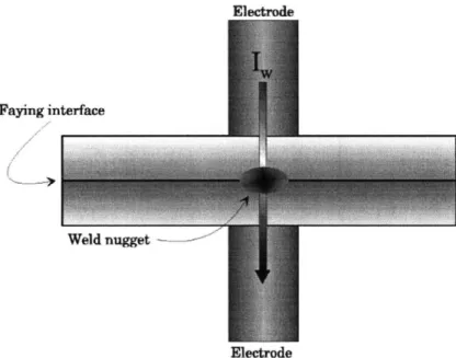
Electrode
Faying interface
Weld nugget - I
Electrode
Figure 3.8: Schematic of weld junction.
3.6.2
Spot welding
Electrical or resistance welding was pioneered in the late 19th century by Elihu Thompson. Thompson took advantage of the fact that an electrical current evolves heat in any resistive material it passes through.
For constant-current welding the heat evolved,
SQ,
has the formI A (3.3)
where I, is the weld current, R is the weld junction resistance, A is the weld junction area, and ft is the weld time.
The welding apparatus is arranged so that most of the weld power is dissipated at the faying interface, which is the junction of the materials to be welded. Inspection of the heat evolution equation reveals that for a given weld current and time, the weld heat increases directly as the junction resistance and inversely as the junction area. This suggests that the resistivity of the weld
path should be concentrated at the weld junction, and that the junction area should be small. Resistive heating is only part of the story, however. While a large area of contact is desirable between the electrodes and the workpiece to reduce heating at those points, a small electrode-workpiece
32 CHAPTER 3. FABRICATION TECHNIQUES
0
5
7
17
22
24
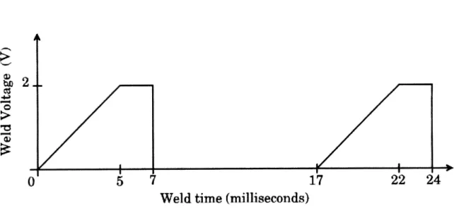
Weld time (milliseconds)
Figure 3.9: Schedule for welding CuSnPb leadframe to steel fiber bundle.
junction area is preferred to reduce heat diffusion from the faying interface.
When two uniform, smooth pieces are welded together, the heating will be greatest along the center axis of the applied current, and a weld will form between the pieces along this axis. The heating is greatest along the center of this axis, because at that point the weld is most surrounded by heated material.
Different types of welds will arise from different levels of heating. The "coldest" welds form when the grain boundaries of the workpieces shift and flatten to form large interfaces. As heating increases, grain boundaries shift and dovetail, forming a complex interface. Still greater heating results in a breakdown of grain boundaries and a variable alloying of the materials making up the junction.
The leadframe used in this case was copper (Cu) plated with a tin-lead (SnPb) alloy. Diffusion alloying takes place at the Cu - SnPb interface, and the result after several hours is a Cu - CuSn
-SnPb interface. This chemistry is common to the process of soldering with -SnPb alloys on Cu or CuSn surfaces.
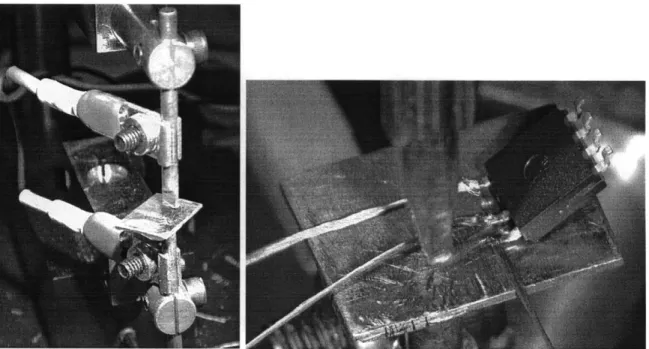
Weld schedules are often difficult to optimize, and depend crucially on many factors including electrode geometry, contact area, and electrode-workpiece metallurgy.
For the present work, weld schedules have been developed to maximize the pull strength of the thread-leadframe junction.
To prevent interference that would be caused by fraying of the end of the fiber bundle, it is first welded flat by one or two weld operations. The tab is then cut in the middle and the excess length is discarded. To weld this tab to the leadframe, the tinned copper leadframe (Cu/SnPb) is placed on
3.6. THE PLASTIC THREADED CHIP CARRIER
Figure 3.10: Welding electrode configuration.
the lower electode, the steel fiber bundle tab is placed on top of the lead, and the upper Cu electrode is brought down to weld the tab to the lead at an applied force of 16 lbs.
Other weld schedules, geometries, and electrode materials have been tried with varying degrees of success. To minimize the number of tool changes necessary during weld process development, an electrode geometry has been chosen to simulataneously provide a good mix of thermal, electrical, and mechanical properties, and is shown in Figure 3.10.
The upper electrode is formed from
}inch
diameter copper rod stock, with the end ground to a'inch x 1 inch rectangular cross section. The lower electrode is formed of linch copper rod with
a linch x !inch x
ninch
copper "anvil" soldered on top. The anvil provide a thermal sink which draws excess heat away from the weld, decreasing the likelihood of electrode sticking and promoting even heating of the weld joint.3.6.3
Weld evaluation
The mean shear strength of a weld formed according to the above procedure is 36.8 N (o- = 4.3 N, n = 9), determined by pull testing. Welds with a pull strength less than 10 N were discarded (3 out of 12 samples tested) as resulting from poor process control or weld contamination. During these
CHAPTER 3. FABRICATION TECHNIQUES
Figure 3.11: Top view of a stainless steel thread welded to Cu/CuSnPb lead.
tests, most failures occurred at the point where the leadframe entered the plastic package, not at the thread-leadframe weld itself.
A pull strength of 36.8N (or equivalently, 8.251b) is more than sufficient for the application de-scribed above, e.g. that of welding steel threads to leadframe stubs prior to encapsulation in a hermetically-sealed plastic package. It should also suffice for the purposes of prototyping such pack-ages, where steel yarn is welded to the leads of an existing package and the resulting construction is encapsulated in epoxy. In both of these applications, the pull strength of the original weld is
augmented by the threads' adhesion to the package encapsulant, and the compressive constraint the package itself imposes on the weld junction.
3.7
E-broidered circuitry
Once the components are packaged, they are sewn onto an insulating fabric substrate with embroidered conductive traces. The traces themselves are sewn in a composite yarn, spun from a mixture of 95% Nomex fibers and 5% steel fibers, where the average fiber length is about 3 cm. The fine structure of this yarn is shown in two views in Figure 3.13.
A composite yarn of this sort is used because the all-steel thread used to form component leads cannot be sewn by ordinary processes, comprising as it does a bundle of some hundred
continuously-3.7. E-BROIDERED CIRCUITRY
Figure 3.12: Optical micrograph of Cu-steel weld junction.
drawn steel fibers. As a thread is sewn into fabric, tensions are imposed unevenly over its cross section. Threads spun from short (staple) fibers are able to accomodate this variation in tension by stretching more on one side than the other, and manage to rebalance the tension after a short stretch of thread. Uneven stresses propagate only over short distances in staple yarns.
Contrast this with the continuously drawn steel fiber bundle, in which individual fibers are meters (rather than centimeters) long. Stresses are no longer local to a small region of sewing, and tensions rapidly mount without resolution, resulting in bunching of the thread as it feeds through the sewing machine. Some of the bunched threads will eventually twist into an obstruction that will not pass through the sewing needle's eye, and the entire process will grind to a halt.
An alternative to the continuously drawn steel fiber bundle might be an all-steel yarn spun from short steel fibers. Care would have to be taken to choose the length of the fibers to balance the effects of stress propagation over long distances against the tendency of the fibers to not interlock over short distances because of their stiffness.
The particular composite yarn used here is known as Bekintex, and is manufactured by Bekaert Fibre Technologies. Bekaert Fibre produces a variety of composite textiles which incorporate finely drawn metal fibers to obtain particular bulk properties of electrical conductivity, thermal conductivity, surface finish, and tensile strength.
CHAPTER 3. FABRICATION TECHNIQUES
Figure 3.13: Optical micrograph of stainless/Nomex composite thread (Bekintex 50/2). 20 pm stain-less teel fibers are visible as dark lines in the lighter-colored Nomex matrix that forms the bulk of the yarn. This two-ply yarn is approximately 0.010 inch in diameter.
3.7. E-BROIDERED CIRCUITRY
Bekaert credits a 1936 U.S. Patent [Eve36] with the original description of the process whereby a bundle of fine metal fibers may be drawn continuously and simultaneously from source metals. Bundle drawn fibers can be produced in many different morphologies by translating the polymer-based methods of the synthetic textile industry into their metallurgical equivalents. Continuous and broken bundles, cut fibers, spun yarns, threads, etc. are all produced in this way.
The fibers themselves are available in diameters from 100pam down to 12pLm, and as far down as to 2im for very metallurgically clean (free of large inclusions) alloys. Alloys commonly used in these processes include Stainless 316L steel, Stainless 302 steel, Inconel 601, Nichrome, FeCr alloy, and Titanium [Tec97]. These 100% metal fiber yarns are used in knitting, weaving, needlepunching, and braiding processes, with sewing and embroidery being notable omissions from the list.
Bekaert cites the primary applications for these materials as being filter media, antistatic textiles, heat-resistant textiles, burners, and conductive plastics. Their product range includes 100% metal fiber products as well as blends of metal fibers combined with natural or man-made fibers [Tec97].
Steel threads were chosen for their strength, resistance to corrosion, biological inertness, and ready availability in textile form at low cost. The major drawback of using steel and steel-composite threads is the difficulty involved in attaching them to existing electronic components.
For instance, we might wish to attach steel threads directly to the bondout pads of an IC die without using an intermediate Cu/CuSnPb leadframe. Unfortunately this is impractical for many reasons.
First of all, steel threads are too strong to be thermocompression bonded to metallized pads on a crystalline silicon substrate without causing the substrate to crack [KRT89]. More important however is the metallurgy of bondout pads on silicon chips.
Most ICs use Al metallization for on-chip interconnections, as well as for bondout pads. Nearly all pad-to-leadframe wirebonds take place using Au or Al wire (actually A199% + Sil%). Au is used
more frequently because it requires less pre-forming during the wirebonding procedure and because it forms less of a surface oxide layer than Al wire does. Bondout pads are also usually plated with Au (over the Al) to promote good wire-to-pad bonding.
The Au - Al interface does however represent a compromise between the need to achieve a strong
wirebond and the need to develop a process insensitive to contamination. The most common reliability problem in wirebonding results from the formation of intermetallic compounds at the Au-Al interface, known by their color as "purple plague" (AuAl2) or "white plague" (Au5Al2). These compounds are
very brittle compared to the metallic Au and Al that surround them. As a consequence of this brittleness, wire flexing (as a result of vibration or thermal cycling) more easily induces metal fatigue and stress cracks [KRT89]. These and other intermetallic compounds and alloys deleterious to the strength of the Au - Al interface are known to form more readily in the presence of all of the metals
CHAPTER 3. FABRICATION TECHNIQUES
that Bekaert produces in textile form. It is therefore essential to ensure the purity of the gold used in plating bondout pads, as well as the purity of gold wire used to bond to the gold plated pad.
3.7.1
E-broidered composites
One very useful technique which arises from the attachment technique used here (couching the thread-frame to the fabric with an e-broidered trace) is that of on-the-fly stitching of composite traces. Over the run of the trace which couches the steel thread, the trace's conductivity will be approximately that of the steel thread itself (slightly higher due to the parallel conductivity of the e-broidered trace). There is a difference in conductivity of almost two orders of magnitude between the stainless thread and the stitched Bekintex composite yarn, with typical resistances of 1(/cm and 100Q/cm respec-tively.
This immediately implies that low-tolerance resistors can be constructed simply by patterned stitching of known lengths of Bekintex and Bekinox. It also leads to the more general notion of a composite trace or sensor generated by mixing materials together by means of stitching.
3.8
Implementation of the MIDI Jacket keypad
The MIDI Jacket keypad was built using a PIC microcontroller to perform capacitive measurements of connections to sewn electrodes on a denim substrate. The measurements were implemented almost entirely in software, as an exercise in developing electric field sensors using a minimum of hardware, but this minimalism also benefits the fabric circuit designer by reducing the number of components
(and hence interconnections) that must be incorporated into a circuit.
The keypad has been shown before, in Figure 1.4, while its circuitry and software are detailed in the Appendix. A washable electrode array was sewn into denim using Bekintex thread, in the pattern of a telephone keypad with traces leading from the symbols to an array of connection pads intended to mate with a conventional circuit board.
3.9
Multilayer circuit construction
The leap from single layers of e-broidery to multi-layer circuitry is motivated not only by the desire to develop non-trivial interconnects and circuitry, but also by the need to control the outward appearance of fabric interfaces. Fabric-based user interfaces should at large display only devices and symbols relevant to user interaction, and not the underlying complexity of their implementation.
3.9. MULTILAYER CIRCUIT CONSTRUCTION
leads to the final step of stacking fabric layers with and adding an inter-layer stitched interconnect. The way this is done with conventional circuit boards is to print each layer in copper on one side of a thin substrate, then to laminate the strata together, drilling holes as appropriate and plating with copper to interconnect traces on different strata. The inter-layer connections are commonly referred to as vias, and the metallurgy and chemistry of this process is messy and expensive.
To do the same thing in fabric, however, we have an easier time. Each layer of the interconnect is e-broidered onto its own fabric substrate. Then insulating fabric layers are place between the e-broidered layers, with vias stitched between layers using more conductive thread.
Suppose we want to build an interface which has only buttons on its top surface. How can this be done?
First, we e-broider a plane with nothing but the interface objects sewn in. The next layer is simply a thin, sturdy insulating layer, followed by another layer with e-broidered circuitry. This second layer of circuitry includes pads which line up with the interface symbols on the top layer. The next layer is again an insulator, and the last e-broidered layer includes the components which have had their leads couched onto the the fabric substrate connecting to traces, some of which include pads to connect with other layers. Finally, the layers are assembled and stitched together at points where signals must cross between layers.
To enhance the final appearance, the topmost layer is the last one to be quilted onto the remainder. This avoids sewing vias through the top layer for any connections other than those required by the top layer. The principle is illustrated in Figure 3.14.
CHAPTER 3. FABRICATION TECHNIQUES
-Z
Stitched vias
Chapter 4
Future work
What remains to be done? The present work collects a year's worth of observations and experience with fabric circuitry in a desire to point the way toward scalable processes for the manufacture of washable computing systems. It is expected that the primary uses of such systems will be as interfaces to more commonplace devices, such as pagers, phones, and wearable computers.
The two biggest questions that arise in connection with this work are "Can you wash it?" and "What if you want to wear a different outfit?" The present work addresses the first question directly, and the second indirectly.
Regarding washability, e-broidery will not currently function when it is wet, but it works fine once it is dry again. Whether the wetting agent is rain, isopropyl or ethyl alcohol, or one of the common dry-cleaning fluids, once the e-broidered circuit is dry it functions as specified. Although rigorous testing remains to be done, the early indications are very promising. Even human sweat (a mildly corrosive saline condensate) does not appear to harm e-broidery even over many cycles of exposure, while it does in fact corrode conventional tinned-copper printed circuitry. Moreover, if a conventional circuit board gets wet during operation, solder will be seen to dissolve sufficiently into the water to form aggregates along electric field lines in the water, causing shorts to form. E-broidery does not appear to be subject to this mechanism, although further testing of the steel threads is on the agenda. The threadframe prototypes have been surprisingly robust, and further work should be done to characterize their integrity over multiple stress cycles. Since the stainless threads used in this work are composed of many long, thin fibers, we would like to know how often an individual fiber is likely to break when the thread or the entire structure holding it is subject to stress.
As for the issue of changing outfits, this is an open research question that might be best addressed by ongoing efforts into building environments that support mobile agents in embedded applications.