HAL Id: hal-02332912
https://hal.archives-ouvertes.fr/hal-02332912
Submitted on 25 Oct 2019
HAL is a multi-disciplinary open access
archive for the deposit and dissemination of
sci-entific research documents, whether they are
pub-lished or not. The documents may come from
teaching and research institutions in France or
abroad, or from public or private research centers.
L’archive ouverte pluridisciplinaire HAL, est
destinée au dépôt et à la diffusion de documents
scientifiques de niveau recherche, publiés ou non,
émanant des établissements d’enseignement et de
recherche français ou étrangers, des laboratoires
publics ou privés.
Predictive modelling of the dielectric response of
plasmonic substrates: application to the interpretation
of ellipsometric spectra
Alessandro Pugliara, M Bayle, Caroline Bonafos, Robert Carles, Marc
Respaud, K Makasheva
To cite this version:
Alessandro Pugliara, M Bayle, Caroline Bonafos, Robert Carles, Marc Respaud, et al..
Predic-tive modelling of the dielectric response of plasmonic substrates: application to the interpretation
of ellipsometric spectra. Materials Research Express, IOP Publishing Ltd, 2018, 5 (3), pp.035027.
�10.1088/2053-1591/aab32b�. �hal-02332912�
PAPER
Predictive modelling of the dielectric response of plasmonic
substrates: application to the interpretation of ellipsometric spectra
A Pugliara1,2 , M Bayle3 , C Bonafos2 , R Carles2 , M Respaud4,5 and K Makasheva1
1 LAPLACE, Université de Toulouse; CNRS, UPS, INPT; 118 route de Narbonne, F-31062 Toulouse, France
2 ‘Nano-optics and nanomaterials for optics’ group-CEMES-CNRS, Université de Toulouse, 29 Jeanne Marvig, BP 94347, F-31055
Toulouse, France
3 Institut des Matériaux Jean Rouxel(IMN), Université de Nantes, CNRS; 2 rue de la Houssinière, BP 32229, F-44322 Nantes Cedex 3,
France
4 LPCNO, Université de Toulouse, CNRS, INSA, UPS; 135 Ave Rangueil, F-31077 Toulouse, France 5 AIME, Université de Toulouse, INSA, UPS, INPT; 135 Ave Rangueil, F-31077 Toulouse, France
E-mail:kremena.makasheva@laplace.univ-tlse.fr
Keywords: plasmonic substrates, modelling, spectroscopic ellipsometry, AgNPs embedded in SiO2layers
Supplementary material for this article is availableonline
Abstract
A predictive modelling of plasmonic substrates appropriate to read ellipsometric spectra is presented
in this work. We focus on plasmonic substrates containing a single layer of silver nanoparticles
(AgNPs) embedded in silica matrices. The model uses the Abeles matrix formalism and is based on the
quasistatic approximation of the classical Maxwell-Garnett mixing rule, however accounting for the
electronic confinement effect through the damping parameter. It is applied on samples elaborated by:
(i) RF-diode sputtering followed by Plasma Enhanced Chemical Vapor Deposition (PECVD) and (ii)
Low Energy Ion Beam Synthesis
(LE-IBS), and represents situations with increasing degree of
complexity that can be accounted for by the model. It allows extraction of the main characteristics of
the AgNPs population: average size, volume fraction and distance of the AgNPs layer from the matrix
free surface. Model validation is achieved through comparison with results obtained from
transmission electron microscopy approving for its applicability. The advantages and limitations of
the proposed model are discussed after eccentricity-based statistical analysis along with further
developments related to the quality of comparison between the model-generated spectra and the
experimentally-recorded ellipsometric spectra.
1. Introduction
The properties and potentialities of nanocomposite materials are nowadays widely studied aiming at a very broad spectrum of applications. It is difficult to deny the usefulness of nanocomposite materials for electronic devices and electrical engineering solutions, asflame retardant of natural and synthetic textile polymers or for medical purposes as antibacterial agents[1–6and the references therein]. Moreover, nanostructures containing
a layer of gold or silver nanoparticles(AgNPs) embedded in silica matrices close to the free surface have strong potential for plasmonic devices. The main advantage of these structures is the possibility to manipulate, localize and enhance the electromagneticfield at their surface [7,8]. The Localized Surface Plasmon Resonance (LSPR)
of metallic NPs is widely explored for enhanced optical spectroscopies of molecules[9,10], photothermal
therapy[11], photovoltaics [12], or more recently in plasmoelectronics [13] and photocatalysis [14].
Presently, visualisation and characterisation of nanocomposite materials is mostly accomplished by using well-established microscopy techniques, including Atomic Force Microscopy(AFM), Scanning Electron Microscopy(SEM) and Transmission Electron Microscopy (TEM) and their derivative modes. Although being extremely performant these characterisation methods remain‘local’, intrusive, and unsuitable for real-time and in-line monitoring of the processes, especially on the surface/interfaces modifications. To guarantee the
performance of plasmonic structures when integrated in devices one needs to characterize their dielectric response during the elaboration phase. A good way is to use reliable non-destructive diagnostic methods. Many fundamental and functional properties of nanocomposites can be conveniently probed using several variants of optical spectroscopy. In particular, using polarized light in ellipsometric measurements proves to be highly efficient. Spectroscopic ellipsometry (SE) actually turns out to be the most appropriate among various tools for characterization of nanocomposite materials[15–17]. The SE is a destructive, intrusive, and
non-invasive, contactless optical technique that has been developed and applied extensively over many years now. The SE is widely used for measurements of the thickness and optical constants of semi-transparent dielectric, semiconductor, and metal thinfilms. It is a very powerful diagnostic method not only for optical
characterization of bulk materials and thinfilms, but also for in situ real-time measurements of multilayered film structures, interfaces, and composites, during fabrication and processing. However, to fully benefit the
advantages offered by SE an appropriate modelling necessary for interpretation of the recorded spectra is highly demanded. The application of SE, especially on the sub-100 nm thickness range and/or on absorbing
heterogeneous structures like plasmonic substrates, should be carefully performed in order to limit the errors in the interpretation of the recorded spectra. A critical review discussing how to reduce the correlation between film thickness and optical constants was recently provided in the literature [18]. It gives an assessment of
advantages and limitations in applying optical diagnostic methods when dealing with very thin and absorbingfilms.
In this work we report on development, test and application of a predictive model appropriate for interpretation of ellipsometric spectra recorded on plasmonic substrates containing AgNPs. It is based on the quasistatic approximation of the classical Maxwell-Garnett mixing rule applied with Abeles formalism and accounts for the electronic confinement effect through the damping parameter. Model validation is achieved through comparison with results obtained from transmission electron microscopy. The intended application of the model is related to fast tracking of plasmonic substrates needed to study the underlying mechanisms for adhesion of biological targets(proteins/cells) on dielectric matrices containing AgNPs with specific attention paid to the controlled release of silver from those structures[19].
2. Experimental
2.1. Sample description
The plasmonic substrates reported here consist of a delta-layer of AgNPs embedded in silica matrix at a well-controlled nanometric distance from the free surface. Their total thickness was selected in a way that for specific wavelengths the reflectance is at minimum and consequently the electric field at the free surface is at maximum, as accounted for by modelling the propagation of electromagnetic waves in stratified media [20,21]. In the
current study a total thickness of 100 nm of the nanocomposite structures was intended. The selected samples actually represent situations with increasing degree of complexity that can be accounted for by the model. The reason for such presentation is limited to practical issues. The presented samples were elaborated by using two different but complementary physical deposition methods:(i) RF-diode sputtering followed by Plasma
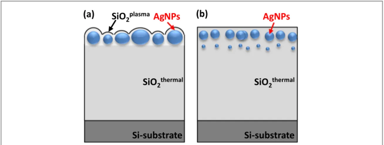
Enhanced Chemical Vapor Deposition(PECVD) for samples S1 and S2, and (ii) Low Energy Ion Beam Synthesis (LE-IBS) for samples S3 and S4, called hereafter ‘plasma deposited’ and ‘implanted’ samples, respectively. The twofinal structures are schematically represented on figure1.
Several differences in the resulting plasmonic structures induced by the corresponding elaboration technique are intentionally put forwards on the pictures for clarity. In general, the plasma deposition processes are known to be conformal to the surface on which the layer is deposited. This surface conformity allows coatings of patterned substrates. In this study, as the plasma deposited SiO2cover layer is very thin, it envelops the AgNPs and spreads between them,finally imposing a slight waviness on the surface (figure1(a)). The ion
implantation process preserves the composition of the host matrix and respects the planarity of the surface of the final structure. However, for some synthesis conditions it may give rise to a secondary plane of smaller in size AgNPs placed deeper in the silica matrix in comparison to the main layer of AgNPs(figure1(b)). Detailed
description of the methods, elaboration procedure and characterisation of the sample properties are given elsewhere[22–27]. The two synthesis methods and the operating conditions are summarized in supplementary
information(SI) which is available online atstacks.iop.org/MRX/5/035027/mmedia. 2.2. Structural and optical characterization of the plasmonic substrates
Structural characterization of the deposited nanostructured layers was carried out by applying various diagnostic methods. Visualization of the plasmonic substrates was achieved by TEM in cross-sectional(XS-TEM) and plane view(PV-TEM). Specimens transparent to electrons have been prepared according to a standard procedure: mechanical polishing and Ar+ion milling. The observations were performed using afield emission
TEM, FEI Tecnai™ F20 microscope operating at 200 kV, equipped with a spherical aberration corrector and the Gatan Imaging Filter(GIF) TRIDIEM.
The experimental ellipsometric spectra were acquired with a SOPRA GES5 spectroscopic ellipsometer in the wavelength range from 250 to 850 nm at incidence angle of 75°.
Systematic comparison of the obtained results from ellipsometry with results from TEM analyses allows identification of real situations that can be considered by the model.
3. Description of the theoretical model used for simulation of plasmonic structures
The optical frequency range(3×10¹¹Hz<ω/2π<3×1016Hz) extends from far-infrared (FIR) to vacuum-ultraviolet(VUV) spectral regions with longest and shortest wavelength of 1 mm and 10 nm, respectively. At the optical frequencies and below(microwave and radiofrequency range) matter behaves as continuum since the atomic dimensions are of the order of 0.1 nm. The response at macroscopic level is smooth and usually detected by light probes in the optical range although the discrete atomic structure of matter and the induced strong spatial variations of the quantities describing the opticalfields. The nanostructured materials can be considered as a mixture of individual components each of them possessing their own continuum-like optical response. The advantage of treating a nanostructured material as a mixture having continuum behavior is the possibility tofind the macroscopic (averaged) field quantities by using approximate treatment (effective media approximation, EMA). If the composite material consists of dissimilar regions that are small compared to the wavelength of probing light but large enough to express their own dielectric identity, the localfields and the subsequently obtained averaged quantities are impacted by the presence of screening charge that develops at the boundaries between the regions[28]. The screening charge modifies locally the electric field which yields
modifications in the averaged macroscopic polarization. However, under certain conditions we can find the dielectric function, but the one that describes the macroscopic response of the nanocomposite material to the appliedfield. If the geometry of the nanostructured material is sufficiently simple so that we can solve the Maxwell equations analytically, we can obtain expression relating the averaged dielectric function to the structural parameters of the nanocomposites on the basis of EMA. We have performed such treatment on the nanocomposites elaborated in this work and described the above plasmonic structures by using the prototype of EMA, the one developed by Garnett[29].
The physical situation that we describe consists of an ensemble of AgNPs inserted in a silica matrix at a given distance from the free surface. Following the EMA rules, and in particular the Maxwell-Garnett approximation, we convert this heterogeneous system in a homogeneous effective media. To describe the interaction between the AgNPs and the electromagnetic wave we limit the case to the quasi-static approximation. This consideration is based on the fact that the size of AgNPs in the system is much smaller than the wavelength of the external electricfield in the visible range. Additional condition is that the density of AgNPs inclusions (their volume fraction) remains small so that their impact on the system can be considered as a perturbation only. Accordingly, the electromagneticfield does not experience the detailed structure of the nanocomposite. The effective
permittivity of the mediaεeffis then available according to the Clausius-Mossotti relation where N is the number of NPs with volume V, the volume of one particle, andεmis the dielectric permittivity of the host matrix:
Figure 1. Schematic representation of the studied plasmonic structures prepared by:(a) RF-diode sputtering followed by PECVD and (b) LE-IBS.
N 2 3 . 1 eff m eff m m e e e e a e -+ = ( )
After introducing the volume fraction of AgNPs f=NV in the silica matrix and by replacement of the polarizabilityα by its expression for NPs of spherical shape [29] one finds the general expression of
Maxwell-Garnett: f 2 2 , 2 eff m eff m NP m NP m e e e e e e e e -+ = -+ ( )
withεNPrepresenting the dielectric permittivity of the nanoparticles.
For sufficiently small volume fractions ( f=1), i.e. far from percolation threshold, the effective permittivity of the mediaεefftakes the form:
f 3 2 . 3 eff m m NP m NP m e e e e e e e = + -+ ( )
When scaling down to nanometer size, the optical response of metals is affected by three main features: size, shape and surrounding medium of the metal[30,31]. The complex dielectric function of metal nanoparticles
develops size dependency for nanoparticles of dimensions in the nanometer range. The size dependency of the dielectric function stems from both interband transitions and damping contributions. The impact of interband transitions is related to local changes in the properties, like electron density and atomic distances, close to the particle surface, for example. The damping contribution involves changes in the electronic mean free path due to the scattering of conduction electrons against the nanoparticle surface. Usually, the latter contribution exceeds the former one by far more[32]. Consequently, when the nanoparticle size is smaller than the bulk electronic
mean free path lb(52 nm for silver [30]), the damping increases and can be written as:
D g v D , 4 NP b s F NP g( )=g + ( )
whereγbis the bulk dumping parameter accounting for collisions of electrons with other electrons, crystal lattice (phonons), lattice defects, or impurities; γb=1/τ where τ is the time between two consecutive collisions (known as the relaxation time of the free electron gas), gsis a dimensionless parameter depending on the surface scattering[33,34], taken as a constant (gs=1) in the present modelling, vFis the Fermi velocity, and DNPis the nanoparticle size. In the visible frequency range, the conditionω?γ (DNP) remains valid and the reale¢ ( )NP w
and imaginaryeNP (w,DNP)components ofεNP(ω, DNP) read:
, 5 NP IB p 2 2 e w e w e w w w ¢ ( )= ¢( )@ ¢ ( )- ( ) D g v D , . 6 NP NP p s F NP 2 3 e w e w w w ( )@ ( )+ ( )
Consequently, the size dependency of the dielectric function is negligible for the real component of the dielectric function(which is equal to the bulk value) meanwhile it significantly influences its imaginary part.
Finally, the complex dielectric function of spherical metallic nanoparticlesεNP(ω, DNP) can be written as:
D i D , , 7 NP NP IB p NP 2 2 e w e w w w g w = -+ ( ) ( ) ( ) ( )
whereεIB(ω) is the part of the complex dielectric function due to the interband transitions in bulk metals. Considering the dielectric permittivity of the nanoparticles as given by equation(7) in the expression of effective
permittivity of the media(equation (3)) allows for accounting the size effects imposed by the AgNPs in the
theoretical model of plasmonic structures.
4. Numerical procedure for the simulations
Schematic representation of the modeled plasmonic structures is given infigure2. The plasmonic structures are considered as multi-layer systems. Each of the layers is described by its own dielectric permittivity. The layers containing AgNPs are considered as effective media in the frame of the above described Maxwell-Garnett approximation and represented by the corresponding effective dielectric permittivity(equation (3)). As can be
noticed onfigure2such consideration of the plasmonic structure offers the possibility to describe double layer of NPs with different size and volume fractions. This stratified structure is well adapted to account for different physical situations that can arise in the stack representation according to the type of applied elaboration method.
The dielectric properties of the Si-substrate were taken from[35] for the whole wavelength range, those of
equation(7) by using the optical properties of bulk silver [35]. As input parameters in the model we start with
guesses for the thicknesses of different layers in the structure and the corresponding volume fractions of AgNPs. After convergence of the model calculations the output parameters of the simulation are as listed infigure2
along with the calculated ellipsometric spectra(tan (Ψ) and cos (Δ)) in the 250–850 nm wavelength range, corresponding to the considered structure. Those theoretically-obtained spectra are compared with experimentally-recorded ellipsometric spectra on the same sample.
The developed numerical code runs on Matlab software[37] and uses Abeles formalisms for calculations of
the electricfield in multilayer systems. The Abeles formalism is a transfer-matrix method mainly used in computational optics to easily calculate the specular reflectivity of stratified media. The reflection and
transmission of light at the interfaces are calculated using Fresnel equations. More information on the basis and the adopted hypotheses is given elsewhere[21,38,39].
Systematically the parameters of tested plasmonic structures obtained from modelling were compared with results extracted from TEM observations of the same sample.
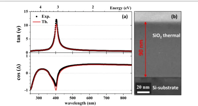
Before going further in the modelling of plasmonic substrates we have used a 90 nm thick SiO2layer thermally grown on Si-substrate as a model benchmark. The obtained from modelling results are shown in figure3(a) along with the experimentally recorded spectra. The obtained from modelling thickness of the SiO2 layer is 89.8±0.5 nm. The XS-TEM image of the studied benchmark sample is shown in figure3(b) as
complementary indicator for comparison of the obtained SiO2layer thickness. It confirms the theoretically obtained thickness after modelling. Additional verification for the benchmark sample was performed by using the EMA model for ellipsometric spectra processing on WinElli Software available by SOPRA[36]. This
test-sample approves the theoretical model and the selected numerical procedure.
Several indicators were used to estimate the sensitivity and uniqueness of the model. Thefirst estimate is related to quality of the comparison between the model-generated ellipsometric spectra and the experimentally obtained ones in the entire spectral range. In particular, the results interpretation is related to the theoretical model sensitivity. This includes calculation of the mean square error(MSE) curve that quantifies the difference between model and experience for all regressed quantities according to:
MSE L M L M 1 2 1 2 , 8 i L i i i i i i 1 mod exp , exp 2 mod exp , exp 2 2
å
y s y s c = -+ D - D = -y = D ⎡ ⎣ ⎢ ⎢ ⎛ ⎝ ⎜⎜ ⎞⎠⎟⎟ ⎛⎝⎜⎜ ⎞⎠⎟⎟ ⎤ ⎦ ⎥ ⎥ ( )wheresexpy D, are the experimental error bars, L and M are the number ofψ, Δ pairs and the number of fit parameters, respectively. Moreover, an uniqueness test of the model was performed to guarantee the less than 10% Unique Range which spans above and below the bestfit that provides 10% variance on the global MSE
Figure 2. Schematic representation of the stratified structure considered for modelling and the parameters of the plasmonic substrates extracted from the simulation.
minimum when compare theoretical and experimental ellipsometric spectra. The normalized MSE versus thickness for the benchmark SiO2sample is given onfigure4.
Similar uniqueness tests were performed on the other parameters extracted from the model of plasmonic structures like size of the AgNPs, their volume fraction, the cover layer thickness, etc. The obtained limits are reported in the next section when discussing the studied plasmonic structures.
5. Results and discussion
5.1. Advantages of the model describing the dielectric response of plasmonic structures
Two physical methods were used to elaborate the plasmonic structures. They are different regarding their basic principles but complementary in terms offinal results. The advantage is above all the possibility to cover different architectures of the nanostructures, evolution of the size, density and shape of the AgNPs and the nanometric distance from the sample free surface.
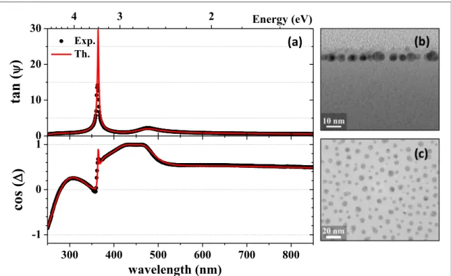
Figure5(a) represents the obtained from modelling and the experimentally recorded ellipsometric spectra
on the plasma deposited sample S1. The XS-TEM and PV-TEM of this sample are shown infigures5(b) and (c),
Figure 3. Benchmark of the model:(a) ellipsometric spectra of 89.8±0.5 nm thick pristine SiO2layer grown on Si substrate as
recorded experimentally(dots) and as obtained from modelling (red line), and (b) XS-TEM Bright Field image of the pristine SiO2
layer.
respectively. The parameters characterizing the plasmonic structure obtained from modelling and those extracted from TEM-image processing are summarized in table1.
The planarity of the AgNPs layer in this case allows for model-generated ellipsometric spectra identical to the experimentally recorded ones. The very slight waviness of the sample surface imposed by the plasma deposition method does not lead to depolarization of the probe light in the entire wavelength range. This particular situation is common for the plasma deposition method and inevitable when the cover layer is very thin, as in the present case. However it can be considered by the model.
The represented plasmonic structure onfigure6corresponds to the implanted sample S3. A strong particularity of sample S3 is the presence of a second plane of AgNPs in-depth of the sample. It arises frequently in the LE-IBS. In this case the constituent layers of the modeled structure arefive, as represented in figure2. This sample testifies for the appropriateness of the developed theoretical model with respect to the stratified structure comprising effective media with different size and volume fraction of the AgNPs.
One can notice the excellent agreement between the parameters describing the two plasmonic structures(S1 and S3) obtained from modelling of the ellipsometric spectra and those extracted from TEM measurements (table1). The common point of these two examples is that their structural parameters completely satisfy the
hypotheses of the Maxwell-Garnett approximation. The AgNPs are spherical in shape. They are well aligned in a
Figure 5.(a) ellipsometric spectra as recorded experimentally (dots) and as obtained from modelling (red line), and (b) XS-TEM and (c) PV-TEM Bright Field images of the plasma deposited sample S1.
Table 1. Parameters describing the studied samples S1 and S3 as obtained from spectroscopic ellipsometry and from TEM observations.
Sample S1 Sample S3
Parameters SE TEM SE TEM
Layer 1: Cover layer Thickness—tc(nm) 5.7±1.5 4.7±0.5 6.5±4.0 7.0±2.0
Layer 2: AgNPs size—DAgNPs( )1 (nm) 6.2±0.6 6.0±1.0 11.0±1.5 7.0±2.0
Thickness—tAg:SiO2( )1 (nm) 6.2±0.6 6.0±1.0 11.0±1.5 10.0±0.5
Volume fraction of AgNPs—fAg:SiO2( )1 0.17±0.01 0.16±0.02 0.11±0.02 0.13±0.02
AgNPs eccentricity—eε n/a 0.36 n/a 0.35
Layer 3: AgNPs size—DAgNPs( )2 (nm) n/a n/a 4.0±1.0 3.2±0.9
thickness—tAg:SiO2( )2 (nm) n/a n/a 4.0±1.0 4.1±0.5
Volume fraction of AgNPs—fAg:SiO2( )2 n/a n/a 0.017±0.007 0.012±0.002
Layer 4: Silica layer thickness—tSiO2(nm) 74.6±1.7 76.0±4.0 73.0±4.0 69.0±3.0
plane so that they form a single layer in which the thickness of the effective media can be considered equal to the diameter of the AgNPs. The AgNPs volume fraction is small enough and can be considered as perturbation only.
Abrupt variations of the experimentally-recorded ellipsometric spectra(as can be noticed on the figures) arise around 400 nm. It is related to the fact that for an isolated spherical AgNP embedded in silica, the plasmon response(mainly absorption) consists in a sharp line centered at 410 nm. When the shape of the AgNPs undergoes evolution, like for example, from spherical to prolate spheroid, or when the AgNPs interact forming dimers or elongated structures, the 3-fold plasmon mode degeneracy is split in a transverse(at lower wavelength) and longitudinal(at higher wavelength) modes, conveying a shift of the plasmon resonance. When the AgNPs touch the free surface, the dielectric permittivity through the refractive index of the effective surrounding medium is lowered presenting a value in between the ones of silica and air, also leading to a shift of the plasmon response towards the shorter wavelengths. Finally, it is important to note that the presence of very small in size AgNPs is accompanied by a broadening of the plasmonic response, according to equation(4). It is thus expected
that the ellipsometric spectra express strong variation in the corresponding wavelength range between 340 and 440 nm. The above described experimental features are considered, to different extent, by the model-generated spectra and the differences are accounted for by the error bars calculated for each parameter of the plasmonic structure(table1), however remaining in the 10% confidence limit (equation (8)) for all calculated parameters.
One can notice on the results obtained for the implanted sample S3 that under condition of narrow AgNPs size distribution, a small departure from the plane organization of AgNPs in the silica layer can be absorbed by the modelling however remaining in the 10% limit of MSE for all defined parameters. As it is considered in the model that the size of the spherical AgNPs equals the thickness of the mixed layer, the obtained from SE AgNPs size is slightly larger than the one obtained from TEM. In consequence this overestimation leads to a slightly smaller volume fraction determined by the SE compared to the TEM observations and to an increase of the incertitude of the thickness of both the cover layer and the SiO2under layer. Another important issue to consider is the effect of mutual interactions of the AgNPs which in the case of very small particles remains rather low and does not lead to violation of the model hypotheses, because the optical response is essentially dominated by absorption and not at all by scattering[30]. For bigger particles the correction has to be taken into account and
contributes to the explanation of the discrepancies observed between model-generated and experimentally recorded spectra. The obtained excellent agreement confirms that the sensitivity and the limits of the developed predictive modelling of the dielectric response of plasmonic substrates are fully dependent on the model hypotheses when related to the AgNPs size and the thickness of the effective medium(tAg:SiO2).
Figure 6.(a) ellipsometric spectra as recorded experimentally (dots) and as obtained from modelling (red line), and (b) XS-TEM and (c) PV-TEM Bright Field images of the implanted sample S3.
5.2. Critical assessment of the applicability of the model
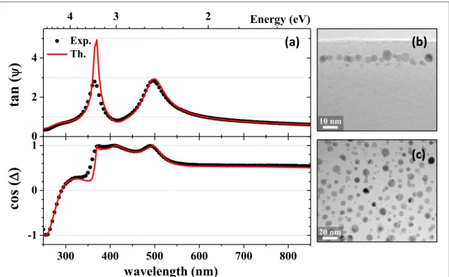
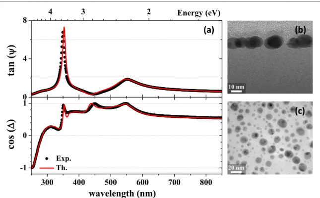
Departure from the hypotheses of the Maxwell-Garnett approximation used in the modelling leads to a strong discrepancy between the model-generated and the experimentally-obtained ellipsometric spectra. This is demonstrated onfigure7for the plasma deposited sample S2 and onfigure8for the implanted sample S4.
The discrepancy occurs mainly in the wavelength range around 400 nm where the localized surface plasmon resonance response is detected. It results from the evolution in shape of the AgNPs from spherical to prolate spheroid for the plasma deposited sample S2 and from dispersion of AgNPs in a band that cannot be represented
Figure 7.(a) ellipsometric spectra as recorded experimentally (dots) and as obtained from modelling (red line), and (b) XS-TEM and (c) PV-TEM Bright Field images of the plasma deposited sample S2.
Figure 8.(a) ellipsometric spectra as recorded experimentally (dots) and as obtained from modelling (red line), and (b) XS-TEM and (c) PV-TEM Bright Field images of the implanted sample S4.
by one or two layers of aligned AgNPs for the implanted sample S4. Additional reasons are the large size-distribution and possible mutual interactions of the AgNPs for both samples(S2 and S4).
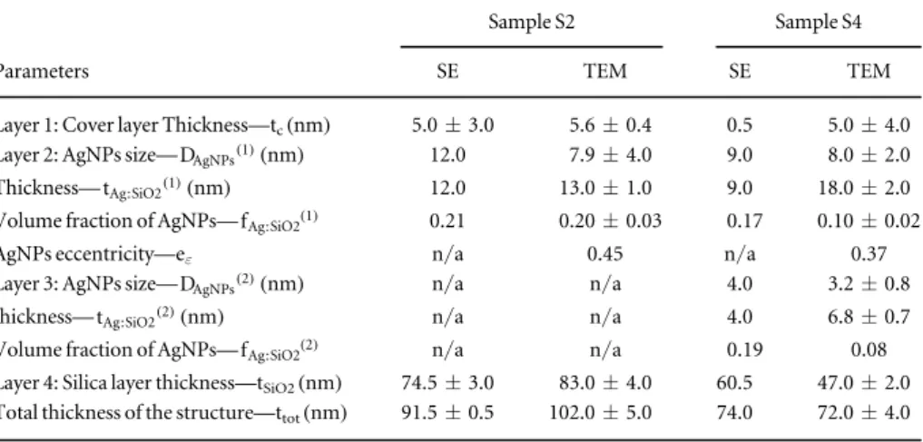
The parameters describing samples S2 and S4 obtained from model-generated ellipsometric spectra and those extracted from TEM images are given in table2. The largest error stems from the AgNPs size as obtained from the model for the corresponding SE spectra and TEM measurements which prevents from correct description of the thickness and dielectric function of the effective media and further reflects on the calculation of the thickness of SiO2layer on which the AgNPs rely. Additional error results from the poor calculation of the SiO2cover layer thickness. Finally, some of the errors accumulate to attain more than 10% difference in the total thickness as for the sample S2 or compensate as for sample S4 but the uniqueness of the solution is not
guaranteed. As given in table2, convergence on few parameters, for which the error bars are reported, can be achieved for the plasma deposited sample S2 but the obtained results are fare from the results obtained after TEM observations. As far as the implanted sample S4 is concerned, no error bars are reported in table2as the structure is beyond the one that can fulfill the model hypotheses and convergence cannot be obtained in this case. The SE reported values for sample S4 should be considered only as indicative.
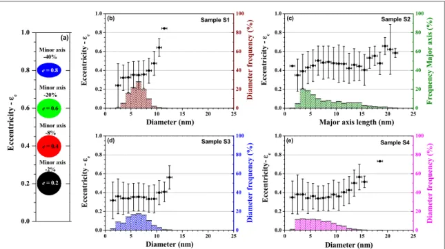
Eccentricity-based statistical analysis of the two plasma deposited samples(S1 and S2) and the two implanted samples(S3 and S4) based on TEM-image processing gives additional information on the influence of the AgNPs shape evolution and size distribution on the theoretically-generated spectra. It underlines the departure from the model hypotheses. The analysis was performed on a large ensemble of AgNPs and is shown infigure9for the four situations discussed here. Statistics on more than 1000 AgNPs have been considered for each sample. The level of eccentricity refers to different shapes of the NPs starting from zero for ideally spherical NPs and evolving to 0.8 for a prolate spheroid shape for which the minor axis is 40% smaller than the major axis(figure9(a)).
The observed excellent agreement between theoretically-obtained and experimentally-recorded ellipsometric spectra is for plasmonic structures(samples S1 and S3) containing AgNPs with shape close to spherical one. The permitted level of eccentricity of AgNPs appears to be limited to 0.4 in order to fulfill the hypotheses of Maxwell-Garnett approximation. This statement is clearly demonstrated onfigures9(b) and (d)
corresponding to samples S1 and S3. Eccentricity level higher than 0.4 is experienced by a very small number of AgNPs: only 29 AgNPs for the plasma deposited sample S1 and only 5 AgNPs for the implanted sample S3. The influence of these AgNPs on the calculation of the effective dielectric function remains limited. Moreover, the size distribution of AgNPs should be quite narrow. As can be seen onfigures9(b) and (d), the plasma deposited
sample S1 and the implanted sample S3 for which the theoretical model describes correctly the plasmonic structures express a narrow size distribution. As far as the plasma deposited sample S1 is concerned, the size distribution of AgNPs in this sample obeys a normal(Gaussian) law with more than 66% of the AgNPs having size in the only±1 nm span around the mean value. The implanted sample S3 presents a size-distribution in good agreement with the theoretical distributions predicted by the Lifshitz–Slyosov–Wagner (LSW) theory for Ostwald ripening, as observed in previous works[25–27]. 72% of the AgNPs in this sample have size in the
±2 nm window around the mean value.
When the evolution in shape becomes important for a large number of AgNPs, like for samples S2(plasma deposited) and S4 (implanted), their dielectric function εNP(ω, DNP) does not fulfill any more the model assumptions. In sample S2(figure9(c)) this percentage is extremely high, 97%. It means that almost all of the
AgNPs in sample S2 change in shape with clearly pronounced evolution towards prolate spheroid. For 8% of the AgNPs in this sample the eccentricity level higher than 0.5. In sample S4(figure9(e)) 10% of the AgNPs have
eccentricity level equal or larger than 0.4.
Table 2. Parameters describing the studied samples S2 and S4 as obtained from spectroscopic ellipsometry and from TEM observations.
Sample S2 Sample S4
Parameters SE TEM SE TEM
Layer 1: Cover layer Thickness—tc(nm) 5.0±3.0 5.6±0.4 0.5 5.0±4.0
Layer 2: AgNPs size—DAgNPs( )1 (nm) 12.0 7.9±4.0 9.0 8.0±2.0
Thickness—tAg:SiO2( )1 (nm) 12.0 13.0±1.0 9.0 18.0±2.0
Volume fraction of AgNPs—fAg:SiO2( )1 0.21 0.20±0.03 0.17 0.10±0.02
AgNPs eccentricity—eε n/a 0.45 n/a 0.37 Layer 3: AgNPs size—DAgNPs( )2 (nm) n/a n/a 4.0 3.2±0.8
thickness—tAg:SiO2( )2 (nm) n/a n/a 4.0 6.8±0.7
Volume fraction of AgNPs—fAg:SiO2( )2 n/a n/a 0.19 0.08
Layer 4: Silica layer thickness—tSiO2(nm) 74.5±3.0 83.0±4.0 60.5 47.0±2.0
Large size distribution of AgNPs leads to ill-defined effective dielectric permittivity of the corresponding layer. This is further confirmed by the analysis presented in figures9(c) and (e). In the deposited sample S2 not
only the shape is prolate spheroid but more than 80% of the AgNPs are in the±4 nm span around the mean value. Although the shape of AgNPs in the implanted sample S4 is close to spherical one(eccentricity level less than 0.4 for the majority of AgNPs) their size distribution evolves to a log-normal one. High eccentricity level combined with large size distribution violates two of the main hypotheses of the model. The AgNPs shape cannot be considered spherical and the thickness of the SiO2layer containing AgNPs cannot be taken equal to the size of the nanoparticles as they are not well aligned.
When the large size distribution is accompanied by eccentricity level over 0.4, the error accumulation in the calculated ellipsometric spectra leads to a large discrepancy of the obtained parameters of plasmonic structures compared to TEM observations and the MSE that quantifies the difference between theoretically-obtained and experimentally-recorded spectra is out of range. These problems that arise from NPs distribution and
eccentricity could be taken into account into our model in order to reproduce the reality of the samples[40,41].
However, the corrections would imply the addition of other adjustment parameters, which may lead to artificially accurate results. The relevance of the developed model relies also on its simplicity and on the limited number of geometrical parameters to describe the plasmonic structures.
6. Conclusions
The results presented in this work concern development, test and application of a predictive modelling
appropriate for interpretation of ellipsometric spectra recorded on plasmonic structures. The model is based on the quasistatic approximation of the classical Maxwell-Garnett formalism and accounts for the electronic confinement effect through the damping parameter. It is found that excellent agreement between theoretically-calculated and experimentally-recorded ellipsometric spectra can be achieved for quasi-spherical AgNPs with volume fraction in the host matrix up to 15%–17%. Eccentricity-based statistical analysis of the samples reveals that a level of 0.4 of the eccentricity of AgNPs should not be exceeded in order to remain in the frame of Maxwell-Garnett approximation. Additionally, a narrow size distribution of the AgNPs is required to allow truthful representation of the thickness of the effective media layer by the diameter of the AgNPs. The simplicity of the proposed model, with a very limited number of adjustment parameters, prevents from artificially accurate results and guarantees the uniqueness of the solution. Possible extension of the model can be envisaged towards consideration of shape evolution and size dispersion of the AgNPs in the description of the dielectric response of plasmonic substrates.
Figure 9. Eccentricity of the AgNPs in the studied samples. Analysis based on minimum 1000 AgNPs per sample. Evolution of the NPs shape for different eccentricity levels in(a); Eccentricity on the left and histogram on the right axis for the plasma deposited samples S1 and S2 in(b) and (c) and for the implanted samples S3 and S4 in (d) and (e).
Acknowledgments
This work isfinancially supported by the program IDEX Transversalité of Université Fédérale de Toulouse (ANR-11-IDEX-0002-02), under project ADAGIO and the CNRS project MI Inter-Instituts. A P acknowledges PhD-grant from Université Paul Sabatier, Toulouse under AO3-project BioNAg.
ORCID iDs
A Pugliara https://orcid.org/0000-0003-1315-1193 C Bonafos https://orcid.org/0000-0001-5140-6690 K Makasheva https://orcid.org/0000-0001-6113-3593
References
[1] Bonafos C et al 2012 Si and Ge nanocrystals for future memory devices Materials Science in Semiconductor Processing15 615–26 [2] Tanaka T 2005 Dielectric nanocomposites with insulating properties IEEE Trans. Dielectr. Electr. Insul.12 914–28
[3] Milliere L, Makasheva K, Laurent C, Despax B, Boudou L and Teyssedre G 2016 Silver nanoparticles as a key feature of a plasma polymer composite layer in mitigation of charge injection into polyethylene under dc stress J. Phys. D: Appl. Phys.49 015304
[4] Norouzi M, Zare Y and Kiany P 2015 Nanoparticles as effective flame retardants for natural and synthetic textile polymers: application, mechanism, and optimization Polymer Reviews55 531–60
[5] Rai M, Yadav A and Gade A 2009 Silver nanoparticles as a new generation of antimicrobials Biotechnology Advances27 76–83 [6] Le Ouay B and Stellacci F 2015 Antibacterial activity of silver nanoparticles: a surface science insight Nano Today10 339–54 [7] Maier S A, Kik P G, Atwater H A, Meltzer S, Harel E, Koel B E and Requicha A A G 2003 Local detection of electromagnetic energy
transport below the diffraction limit in metal nanoparticle plasmon waveguides Nat. Mater.2 229–32 [8] Hartland G V 2011 Optical studies of dynamics in noble metal nanostructures Chem. Rev.111 3858–87
[9] Nie S and Emory S R 1997 Probing single molecules and single nanoparticles by surface-enhanced Raman scattering Science275 1102–6 [10] Jeon T Y, Kim D J, Park S-G, Kim S-H and Kim D-H 2016 Nanostructured plasmonic substrates for use as SERS sensors Nano
Convergence3 18
[11] Baffou G and Quidant R 2013 Thermo-plasmonics: using metallic nanostructures as nano-sources of heat Laser Photonics Rev.7 171–87
[12] Atwater H A and Polman A 2010 Plasmonics for improved photovoltaic devices Nat. Mater.9 205–13
[13] Warren S C, Walker D A and Grzybowski B A 2012 Plasmoelectronics: coupling plasmonic excitation with electron flow Langmuir28 9093–102
[14] Cacciato G, Bayle M, Pugliara A, Bonafos C, Zimbone M, Privitera V, Grimaldi M-G and Carles R 2015 Enhancing carrier generation in TiO2by a synergistic effect between plasmon resonance in Ag nanoparticles and optical interference Nanoscale7 13468–76
[15] Losurdo M et al 2009 Spectroscopic ellipsometry and polarimetry for materials and systems analysis at the nanometer scale: state-of-the-art, potential, and perspectives J. Nanopart. Res.11 1521–54
[16] Tompkins H G and Irene E A (ed) 2005 Handbook of Ellipsometry (Heidelberg: William Andrew: Norwich and Springer) [17] Losurdo M and Hingel K (ed) 2013 Ellipsometry at the Nanoscale (Berlin: Springer)
[18] Hilfiker J N, Singh N, Tiwald T, Convey D, Smith S M, Baker J H and Tompkins H G 2008 Survey of methods to characterize thin absorbingfilms with spectroscopic ellipsometry Thin Solid Films516 7979–89
[19] Pugliara A et al 2016 Assessing bio-available silver released from silver nanoparticles embedded in silica layers using the green algae Chlamydomonas reinhardtii as bio-sensors Sci. Total Environ.565 863–71
[20] Carles R, Farcau C, Bonafos C, BenAssayag G, Bayle M, Benzo P, Groenen J and Zwick A 2011 Three dimensional design of silver nanoparticle assemblies embedded in dielectrics for raman spectroscopy enhancement and dark-field imaging ACS Nano5 8774–82 [21] Bayle M, Benzo P, Combe N, Gatel C, Bonafos C, BenAssayag G and Carles R 2014 Experimental investigation of the vibrational density
of states and electronic excitations in metallic nanocrystals Phys. Rev. B89 195402
[22] Despax B and Raynaud P 2007 Deposition of ‘polysiloxane’ thin films containing silver particles by an RF asymmetrical discharge Plasma Process. Polym.4 127–34
[23] Pugliara A, Bonafos C, Carles R, Despax B and Makasheva K 2015 Controlled elaboration of large-area plasmonic substrates by plasma process Mater. Res. Express2 065005
[24] Makasheva K, Villeneuve-Faure C, Bonafos C, Laurent C, Pugliara A, Despax B, Boudou L and Teyssedre G 2016 Dielectric engineering of nanostructured layers to control the transport of injected charges in thin dielectrics IEEE Trans. Nanotechnology15 839–48 [25] Carles R, Farcau C, Bonafos C, Benassayag G, Pécassou B and Zwick A 2009 The synthesis of single layers of Ag nanocrystals by
ultra-low-energy ion implantation for large-scale plasmonic structures Nanotechnology20 355305
[26] Benzo P, Cattaneo L, Farcau C, Andreozzi A, Perego M, Benassayag G, Pécassou B, Carles R and Bonafos C 2011 Stability of Ag nanocrystals synthesized by ultra-low energy ion implantation in SiO2matrices J. Appl. Phys.109 103524
[27] Benzo P, Bonafos C, Bayle M, Carles R, Cattaneo L, Farcau C, Benassayag G, Pécassou B and Muller D 2013 Controlled synthesis of buried delta-layers of Ag nanocrystals for near-field plasmonic effects on free surfaces J. Appl. Phys.113 193505
[28] Aspnes D E 2011 Plasmonics and effective-medium theories Thin Solid Films519 2571–4
[29] Garnett J C M 1904 Colours in metal glasses and in metallic films Philos. Trans. R. Soc. A Math. Phys. Eng. Sci.203 385–420 [30] Kreibig U and Vollmer M 1985 Optical Properties of Metal Clusters (Berlin: Springer)
[31] Maier S A, Brongersma M L, Kik P G, Meltzer S, Requicha A A G and Atwater H A 2001 Plasmonics—a route to nanoscale optical devices Adv. Mater.13 1501–5
[32] Coronado E A and Schatz G C 2003 Surface plasmon broadening for arbitrary shape nanoparticles: a geometrical probability approach J. Chem. Phys.119 3926–34
[33] Baida H et al 2009 Quantitative determination of the size dependence of surface plasmon resonance damping in single Ag@SiO2
[34] Carles R, Bayle M, Benzo P, Benassayag G, Bonafos C, Cacciato G and Privitera V 2015 Plasmon-resonant Raman spectroscopy in metallic nanoparticles: surface-enhanced scattering by electronic excitations Phys. Rev. B92 174302
[35] Palik E D (ed) 1985 Handbook of Optical Constants of Solids (Orlando: Academic) [36] SOPRA Database 1999 WinElli Software by SOPRA SA Version 3.04
[37] MATLAB Software 2012 The MathWorks Version R2012b
[38] Larivière G P, Frigerio J M, Rivory J and Abelès F 1992 Estimate of the degree of inhomogeneity of the refractive index of dielectric films from spectroscopic ellipsometry Appl. Opt.31 6056–61
[39] Poinsotte F 2006 Son et matière nanostructurée: diffusion Raman et acoustique picoseconde PhD Thesis Université Paul Sabatier France
[40] Giordano S 2003 Effective medium theory for dispersions of dielectric ellipsoids J. Electrostat.58 59–76
[41] Battie Y, Resano-Garcia A, Chaoui N, Zhang Y and En Naciri A 2014 Extended Maxwell-Garnet-Mie formulation applied to size dispersion of metallic nanoparticles embedded in host liquid matrix J. Chem. Phys.140 044705
1
Supplementary Information
Predictive modeling of the dielectric response of plasmonic substrates:
application to the interpretation of ellipsometric spectra
A. Pugliara,
1,2M. Bayle,
3C. Bonafos,
2R. Carles,
2M. Respaud
4,5and K. Makasheva
1,*1
LAPLACE, Université de Toulouse; CNRS, UPS, INPT;
118 route de Narbonne, F-31062 Toulouse, France
2
“Nano-optics and nanomaterials for optics” group-CEMES-CNRS, Université de Toulouse,
29 Jeanne Marvig, BP 94347, F-31055 Toulouse, France
3
Institut des Matériaux Jean Rouxel (IMN), Université de Nantes, CNRS;
2 rue de la Houssinière, BP 32229, F-44322 Nantes Cedex 3, France
4
LPCNO, Université de Toulouse, CNRS, INSA, UPS; 135 Ave Rangueil, F-31077 Toulouse, France
5AIME, Université de Toulouse, INSA, UPS, INPT; 135 Ave Rangueil, F-31077 Toulouse, France
*Corresponding author: kremena.makasheva@laplace.univ-tlse.frThis file includes:
Sections S1 to S2
Tables S3 to S5
References
2
Sections
S1. Plasma deposition process
The plasma deposition process employed for elaboration of plasmonic structures consists of
an axially-asymmetric RF capacitively-coupled discharge maintained at 13.56 MHz at low
gas pressure that successfully combines metal sputtering (PVD) and plasma polymerization
(PECVD) [S1]. It allows a fine control over the size and density of the metal nanoparticles
along with homogeneous dispersion for metallic concentrations from a few percent up to
100% (continuous metallic nanolayer). Detailed description of this plasma process used for
deposition of plasmonic substrates alongside with the general trends in the structure variation
for different operating conditions and the method versatility are given elsewhere [S2, S3].
Here we summarize the operating conditions for the elaboration of the plasmonic substrates in
interest.
The AgNPs single layer was deposited on thermally grown SiO
2thin films on Si
substrates by means of Ag sputtering of the powered electrode (silver target) in argon plasma
sustained at low gas pressure. It was subsequently covered by a high quality very thin SiO
2plasma layer during the plasma polymerization step to form the stack. The selected plasma
operating conditions for the sputtering process leading to the deposition of AgNPs are
presented in Table S1. As mentioned above after the PVD step, the AgNPs plane was covered
by a very thin SiO
2layer deposited in the same plasma reactor. In the latter deposition step,
the plasma is obtained in a mixture of argon (Ar)-hexamethyldisiloxane (HMDSO,
[CH
3]
6Si
2O)-oxygen (O
2) [S2, S3]. The deposition of SiO
2is performed for a fixed deposition
time t (to always achieve the same thickness as the deposition time controls the layers
thickness according to the established deposition rate), at constant RF power P and total
pressure p (Table S2). A strong particularity of our plasma process, which makes it original and
highly efficient, is the pulsed introduction of the HMDSO-precursor. Combined with an
appropriate amount of O
2and relatively high applied power for the plasma polymerization
phase it ensures deposition of high quality plasma silica layers.
S2. Low Energy Ion Beam Synthesis (LE-IBS)
The ion implantation has been performed on a recently developed synthesis technique based
on implantation of Ag
+ions with low kinetic energy (few keV) and doses of few
10
16ions/cm
2. Under those conditions a layer of AgNPs is embedded near the free surface of a
3
SiO
2layer thermally grown on a Si wafer [S4 – S6]. A specifically modified Varian 200A2
implanter was used in order to work in the low energy range. The layers have been implanted
at fixed energy E of the Ag
+ions and with two ion doses D (see Table S3). The ion density
current I plays a key role for the silver diffusion in the silica matrix and has been fixed to
5 µA for all implantations. In the present case the nucleation of AgNPs takes place during the
implantation process due to the high diffusivity of Ag in SiO
2[S7, S8] without the need of
any annealing step [S4, S9, S10].
To recover the matrix damage and protect the AgNPs from fast oxidation [S5] a
post-implantation rapid-thermal-annealing (RTA) was carried out under N
2atmosphere at 500°C
for 30 minutes. The choice of the annealing time and temperature was restricted as to
maintain unchanged the AgNPs size distribution and their position inside the SiO
2matrix.
Therefore, it was demonstrated that by ion implantation technique one can achieve an
accurate tuning of the AgNPs average size, surface density and position with respect to the
free surface. Nevertheless, for implanted doses larger than 3 × 10
16ions/cm
2, sputtering and
diffusion effects towards the free surface limit the amount of Ag that can be introduced in the
dielectric and thus the final average diameter of the formed nanocrystals, that cannot exceed
15 nm [S6].
Tables
Table S3
Parameters used to elaborate AgNPs by sputtering deposition process (PVD).
Sample AgNPs deposition conditions
(PVD step) Applied Power, P [W] Self-bias voltage, Vdc [V] Ar pressure, p [Pa] Ar flow, [sccm] Time, t [sec] S1 10 - 390 5.2 2.8 10 S2 10 - 390 5.2 2.8 30
4
Table S4
Parameters used to elaborate the SiO2 plasma cover layer by PECVD.
Sample SiO2
plasma deposition conditions
(PECVD step) Applied Power, P [W] Self-bias Voltage, Vdc [V] Total Pressure, ptot [Pa] Ar flow [sccm] O2 flow [sccm] HMDSO injection time, ton [sec] HMDSO period, T = ton +toff [sec] HMDSO average flow [sccm] Time, t [sec] S1 120 - 880 7.68 2.8 1.25 3.1 5 0.25 30 S2
Table S5
Parameters used to elaborate the plasmonic samples by ion implantation.
Sample Ag + Implantation conditions Energy, E [keV] Dose, [1016 ions/cm2] Density current, I [µA] Time, t [hours] S3 10 0.715 5 4.5 S4 10 3.8 5 22
References
S1. Despax B, Raynaud P 2007
Deposition of ‘‘Polysiloxane’’ Thin Films Containing
Silver Particles by an RF Asymmetrical Discharge Plasma Process. Polym. 4 127-134
S2. Pugliara A, Bonafos C, Carles R, Despax B, Makasheva K 2015 Controlled elaboration
of large-area plasmonic substrates by plasma process Mater. Res. Express 2 065005
S3. Makasheva K, Villeneuve-Faure C, Bonafos C, Laurent C, Pugliara A, Despax B,
Boudou L, Teyssedre G 2016 Dielectric Engineering of Nanostructured Layers to
Control the Transport of Injected Charges in Thin Dielectrics IEEE Trans.
Nanotechnology 15 839-848
5

![Risiko- & [und] Schutzfaktoren der psychischen Gesundheit humanitärer Einsatzhelfer : eine systematische Literaturübersicht](data:image/gif;base64,R0lGODlhAQABAIAAAP///wAAACH5BAEAAAAALAAAAAABAAEAAAICRAEAOw==)