HAL Id: tel-02152399
https://tel.archives-ouvertes.fr/tel-02152399
Submitted on 11 Jun 2019
HAL is a multi-disciplinary open access archive for the deposit and dissemination of sci-entific research documents, whether they are pub-lished or not. The documents may come from teaching and research institutions in France or abroad, or from public or private research centers.
L’archive ouverte pluridisciplinaire HAL, est destinée au dépôt et à la diffusion de documents scientifiques de niveau recherche, publiés ou non, émanant des établissements d’enseignement et de recherche français ou étrangers, des laboratoires publics ou privés.
Domain wall propagation combining spin-polarized
current and all-optical switching
Boyu Zhang
To cite this version:
Boyu Zhang. Domain wall propagation combining spin-polarized current and all-optical switching. Mesoscopic Systems and Quantum Hall Effect [cond-mat.mes-hall]. Université Paris Saclay (COmUE); Beihang university (Pékin), 2019. English. �NNT : 2019SACLS096�. �tel-02152399�
Propagation des Parois de
Domaines Combinant Courant Polarisé
et Commutation Toute Optique
Domain Wall Propagation Combining
Spin-Polarized Current
and All-Optical Switching
Thèse de doctorat de l'Université Paris-Saclay et de l'Université de Beihang préparée à l'Université Paris-Sud École doctorale n°575 : electrical, optical, bio : physics and engineering (EOBE) Spécialité de doctorat : Physique
Thèse présentée et soutenue à Pékin, le 23 Mai 2019, par
Boyu Zhang
Composition du Jury : Zheng Zheng
Professeur, Université de Beihang Président
Gilles Gaudin
Directeur de recherche CNRS, Grenoble, SPINTEC Rapporteur
Jianhua Zhao
Professeur, Académie chinoise des sciences Rapporteur
Nicolas Vernier
Maitre de conférences, HDR, Université Paris-Saclay Examinateur
Dafiné Ravelosona
Directeur de recherche CNRS, Orsay, C2N Directeur de thèse
Weisheng Zhao
Professeur, Université de Beihang Directeur de thèse
Stéphane Mangin
Professeur, Université de Lorraine, Institut Jean Lamour Co-Directeur de thèse
REMERCIEMENTS
Je souhaite commencer ce manuscrit par adresser mes remerciements sincères aux personnes qui m’ont beaucoup aidé depuis quatre ans et qui ont contribué à l’achèvement de cette mémoire. Cette thèse a été menée dans le cadre de la coopération entre le Centre de Nanoscience et Nanotechnologie (C2N) de l’Université Paris-Saclay, l'Institut Jean Lamour (IJL) de l'Université de Lorraine et le Fert Beijing Institute de l’Université de Beihang.
J’aimerais remercier en premier lieu mes directeurs de thèse Monsieur Dafiné Ravelosona, directeur de recherche CNRS à l’Université Paris-Saclay et Monsieur Weisheng Zhao, professeur à l’Université de Beihang, et aussi mon co-directeur de thèse Monsieur Stéphane Mangin, professeur à l'Université de Lorraine, qui m’ont accueilli dans leur équipe et qui m’ont soutenu tout au long des quatre ans de travail.
Pendant la 1ère année, j’ai acquis des connaissances basiques sur la spintronique et le
magnétisme, déposé des couches minces et mesuré leur propriété magnétique sous la direction de M. Weisheng Zhao. Dès la 2ème année, j’ai commencé des expériences sur
les parois de domaine combinant le courant et le laser sous la direction de M. Dafiné Ravelosona et de M. Stéphane Mangin. Ils m’ont aidé à exploiter des démarches de recherche scientifique et à résoudre des problèmes scientifiques ou administratifs.
Je tiens à remercier sincèrement Prof. Gilles Gaudin de Spintec, Prof. Jianhua Zhao de l’Académie chinoise des sciences, Prof. Nicolas Vernier de l’Université Paris-Saclay, Prof. Zheng Zheng de l’Université de Beihang d’avoir accepté d’être membre du jury de thèse ainsi que pour leurs remarques et discussions très enrichissantes.
Mes remerciements vont tout particulièrement à Prof. Youguang Zhang, Prof. Na Lei, Prof. Xiaoyang Lin, Dr. Jun Du, Dr. Xueying Zhang, Dr. Yong Xu, Dr. Huaiwen Yang et Dr. Yu Zhang, pour leurs suggestions d’orientation des travaux et leurs expertises expérimentales, et à Dr. Gefei Wang pour m’avoir hébergé pendant mes séjours à Orsay.
Mes remerciements vont ensuite à toutes les personnes de l’équipede nanomagnétisme et électronique de spin de l’IJL. Je remercie Prof. Sébastien Petit-Watelot et Prof. Carlos Rojas-Sanchez pour leurs conseils sur les expériences électriques, et Prof. Gregory Malinowski et Prof. Jon Gorchon pour leurs conseils pendant les expériences de laser. Je voudrais exprimer aussi toute ma gratitude à Dr. Laurent Badie, qui m’a guidé tout au long de la fabrication des micro-fils, et à Prof. Stéphane Andrieu et Prof. Michel Hehn, qui m’ont aidé pour déposer des couches minces. Merci à Pierre Vallobra pour son aide précieuse avec la pulvérisation et merci à Filip Schleicher pour la discussion concernant la simulation de commutation tout optique. Un grand merci à Dr. Crosby Soon Chang pour son conseil avec la mesure des propriétés magnétiques. Je tiens à remercier les doctorants: Kosseila Ait-Oukaci, Hamza Bouhani, Alexandre Dekens, Thibaud Fache, Charles Guillemard, Anton Kyianytsia, Gauthier Masset, Maryam Massouras et Thai Ha Pham, pour les bons moments passés ensemble à Nancy, je leur souhaite plein de réussite pour leur thèse.
Je voudrais aussi adresser mes remerciements à Monsieur Nicolas Vernier, professeur au C2N, qui m’a dirigé pour l’expérience de Kerr et donné des conseils sur ma recherche, à Monsieur Sylvain Eimer, ingénieur au C2N, qui m’a enseigné la technique de pulvérisation, à Monsieur Romain Baude, président de l’entreprise APREX solutions, qui m’a aidé pour traiter les données avec le logiciel TRACK, à Mme Sophie Bouchoule, Mme Laurence Stephen et Prof. Eric Cassan de l’école doctorale EOBE pour leur aide lors de l’inscription et la soutenance de ma thèse.
Je tiens à remercier vivement Prof. Eric Fullerton et Prof. Albert Fert pour nos discussions fructueuses.
Je voudrais aussi remercier tous mes amis: Jianying Qin, Shiheng Liang, Xue Gao, Bingshan Tao, Er Liu, Mamour Sall, Salmen Mrahi, You Wang, Qi An, Jiaqi Zhou, Xiaoxuan Zhao, Xiaochao Zhou, Yang Liu, Deming Zhang, Mengxing Wang, Shouzhong Peng, Lezhi Wang, Jiang Nan, Heng Zhao, Runnan Zhou, Kaihua Cao, Qian Shi, Jiaqi Wei, Anni Cao, Zilu Wang, Shaohua Yan, Pan Liu, Junfeng Qiao, Daoqian Zhu, Houyi Cheng, pour leur accompagnement et aide durant ces quatre ans.
Un grand merci à China Scholarship Council (CSC) pour son support de financement pendent mes recherches en France.
Enfin, et surtout, je voudrais remercier ma famille, et particulièrement mes parents, M. Lingjun Zhang et Mme Meihong Dong, qui ont cru en moi et m’ont encouragé et rassuré dans mes moments de doute et face aux difficultés.
Boyu Zhang
TABLE OF CONTENTS
ABSTRACT ... 1
RÉSUMÉ ... 3
GENERAL INTRODUCTION ... 5
CHAPTER 1 BACKGROUND AND STATE-OF-THE-ART ... 8
1.1 MRAM ... 8
1.1.1 STT-MRAM ... 10
1.1.2 SOT-MRAM ... 11
1.2 Dynamics of domain wall motion ... 13
1.2.1 Domain wall and Dzyaloshinskii Moriya Interaction (DMI) ... 15
1.2.2 Domain wall motion regimes ... 19
1.2.3 Current-induced domain wall motion ... 21
1.2.4 Domain wall motion in Co/Ni multilayers ... 23
1.3 All-optical switching ... 24
1.3.1 All-optical helicity-dependent switching in ferromagnetic materials ... 26
1.3.2 Helicity-dependent all-optical domain wall motion in ferromagnetic materials ... 30
1.4 Summary ... 32
CHAPTER 2 EXPERIMENTAL TOOLS AND SAMPLES ... 33
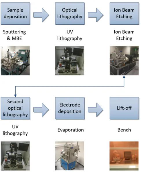
2.1 Sample deposition and fabrication ... 33
2.1.1 Magnetron sputtering ... 33
2.1.2 Molecular Beam Epitaxy (MBE) ... 35
2.1.3 Magnetic characterization ... 38
2.1.4 Optical lithography ... 40
2.1.5 Ion Beam Etching (IBE) ... 41
2.1.6 E-beam evaporation ... 43
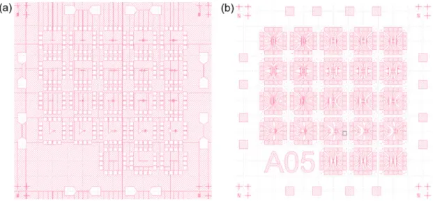
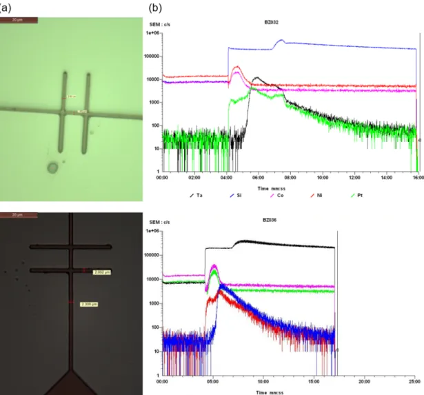
2.1.7 Microwire fabrication ... 43
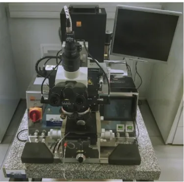
2.2 Magneto-optical Kerr microscopy ... 48
2.2.2 Field configuration for DMI measurement ... 54
2.3 Femtosecond pulse laser ... 55
2.4 Electrical characterization ... 57
2.5 Summary ... 58
CHAPTER 3 MATERIAL EXPLORATION FOR ALL-OPTICAL SWITCHING AND CURRENT-INDUCED DOMAIN WALL MOTION ... 59
3.1 Sputtered Pt/Co/heavy metal (HM) structure ... 59
3.1.1 Magnetic properties ... 59
3.1.2 All-optical switching results ... 61
3.2 Epitaxial Au/Co/Ni/Co/Au structure ... 62
3.2.1 Magnetic properties ... 62
3.2.2 All-optical switching results ... 63
3.3 Sputtered Pt/Co/Ni/Co/Pt structure ... 64
3.3.1 Magnetic properties ... 64
3.3.2 DMI in thin films ... 65
3.3.3 All-optical switching results for thin films ... 66
3.3.4 Criterion for the observation of all-optical switching by domain size calculation ... 67
3.3.5 Current-induced domain wall motion in Ta(3 nm)/Pt(3 nm)/Co(0.3 nm)/Ni(0.6 nm)/Co(0.3 nm)/Pt(3 nm) structure ... 68
3.3.6 Current-induced domain wall motion in Ta(3 nm)/Pt(5 nm)/Co(0.3 nm)/Ni(0.6 nm)/Co(0.3 nm)/Pt(2 nm) structure ... 71
3.3.7 All-optical switching results for microwires ... 73
3.4 Summary ... 74
CHAPTER 4 DOMAIN WALL MOTION COMBINING FEMTOSECOND LASER AND MICROSECOND CURRENT PULSES ... 75
4.1 Combined effect of helicity-dependent optical effect and SOT in Ta(3 nm)/Pt(5 nm)/Co(0.3 nm)/Ni(0.6 nm)/Co(0.3 nm)/Pt(2 nm) structure ... 75
4.1.2 Domain wall motion combining synchronized femtosecond laser pulses
and short current pulses ... 76
4.1.3 Effect of synchronization delay between the electron and light stimuli on domain wall motion ... 79
4.1.4 Energy consumption ... 81
4.1.5 Modeling ... 82
4.2 Combined effect of helicity-dependent optical effect and STT in Ta(3 nm)/Pt(3 nm)/Co(0.3 nm)/Ni(0.6 nm)/Co(0.3 nm)/Pt(3 nm) structure ... 84
4.2.1 Domain wall motion combining synchronized femtosecond laser pulses and short current pulses ... 84
4.2.2 Modeling ... 85
4.3 Domain wall logic based on the combined effect ... 87
4.4 Summary ... 90
CONCLUSIONS AND PERSPECTIVES ... 91
General conclusions ... 91 Perspectives... 92 BIBLIOGRAPHY ... 93 LIST OF ABBREVIATIONS ... 107 LIST OF PUBLICATIONS ... 109 RÉSUMÉ EN FRANÇAIS ... 111
ABSTRACT
1
ABSTRACT
Since the first observation of ultrafast demagnetization in Ni films arising from a pulsed laser excitation, there has been a strong interest in understanding the interaction between ultrashort laser pulses and magnetization. These studies have led to the discovery of all-optical switching (AOS) of magnetization in a ferrimagnetic film alloy of GdFeCo using femtosecond laser pulses. All-optical switching enables an energy-efficient magnetization reversal of the magnetic material with no external magnetic field, where the direction of the resulting magnetization is given by the right or left circular polarization of the light.
The manipulation of magnetization through laser beam has long been restricted to one material, though it turned out to be a more general phenomenon for a variety of ferromagnetic materials, including alloys, multilayers and heterostructures, as well as rare earth free synthetic ferrimagnetic heterostructures. Recently, we have observed the same phenomenon in single ferromagnetic films, thus paving the way for an integration of all-optical writing in spintronic devices.
Moreover, in similar materials, like [Co/Pt] or [Co/Ni] with high spin polarization and tunable perpendicular magnetic anisotropy (PMA), efficient current-induced domain wall (DW) motion can be observed in magnetic wires, where spin-orbit torque (SOT) or spin transfer torque (STT) provides a powerful means of manipulating domain walls, which is of great interest for several spintronic applications, such as high-density racetrack memory and magnetic domain wall logic. However, the current density required for domain wall motion is still too high to realize low power devices.
It is within this very innovative context that my Ph.D. research has focused on domain wall manipulation in magnetic wires made out of thin film with strong perpendicular magnetic anisotropy combining both spin-polarized current and all-optical switching. Different material structures have been explored, in order to investigate the combined
ABSTRACT
2
effects of helicity-dependent optical effect and spin-orbit torque or spin transfer torque on domain wall motion in magnetic wires based on these structures. We show that domain wall can remain pinned under one laser circular helicity while depinned by the opposite circular helicity, and the threshold current density can be greatly reduced by using femtosecond laser pulses. Our findings provide novel insights towards the development of low power spintronic-photonic devices.
Keywords: domain wall, spin-polarized current, femtosecond laser, racetrack memory, spintronics, magnetic multilayered wires
RÉSUMÉ
3
RÉSUMÉ
Depuis la première observation de désaimantation ultra-rapide dans des films de Ni soumis à une excitation laser pulsée, on a assisté à un grand intérêt de comprendre l'interaction entre les impulsions laser ultra-courtes et l'aimantation. Ces études ont conduit à la découverte de la commutation toute optique de l'aimantation dans un alliage de film ferrimagnétique en utilisant des impulsions laser femtosecondes. La commutation toute optique permet un renversement de l’aimantation d’un matériau magnétique sans champ magnétique externe. La direction de l'aimantation résultante est donnée par la polarisation circulaire droite ou gauche de la lumière.
La manipulation de l'aimantation par un faisceau laser a longtemps été limité à un seul type de matériau, mais ce mécanisme s'est avéré être un phénomène plus général qui s’applique à une grande variété de matériaux ferromagnétiques, y compris des alliages, des empilements et des hétérostructures, ainsi que des hétérostructures ferrimagnétiques synthétiques de terres-rares. Récemment, nous avons observé le même phénomène dans des films ferromagnétiques simples, ouvrant ainsi la voie à une intégration de l'écriture toute optique dans les dispositifs spintroniques.
De plus, dans des matériaux de type [Co/Pt] ou [Co/Ni] avec une polarisation de spin élevée et une anisotropie magnétique perpendiculaire contrôlable, un mouvement de parois de domaines induit par un courant polarisé peut être observé dans des pistes magnétiques (couple spin-orbite ou couple de transfert de spin), ce qui présente un grand intérêt pour des applications spintroniques basse consommation et de densité élevée, telles que le concept de mémoire racetrack et la logique magnétique. Cependant, la densité de courant requise pour le mouvement des parois de domaines est encore trop élevée pour permettre la réalisation de dispositifs à faible puissance.
Dans ce contexte innovant, la recherche effectuée dans le cadre de ma thèse s’est concentrée sur la manipulation de parois de domaines dans les pistes fabriquées à partir
RÉSUMÉ
4
de films minces à forte anisotropie magnétique perpendiculaire en combinant à la fois les effets du courant polarisé et ceux de la commutation toute optique. Différents films minces ont été explorés afin d'étudier les effets combinés optiques dépendant de l'hélicité et des couples spin-orbite ou de transfert de spin sur le mouvement des parois de domaines. Nous avons montré que les parois de domaines peuvent rester piégées sous une hélicité circulaire du laser et dépiégées par une hélicité circulaire opposée, et la densité de courant polarisé seuil peut être considérablement réduite en utilisant un laser femtoseconde. Nos résultats sont prometteurs pour le développement de nouveaux dispositifs photoniques-spintroniques de faible puissance.
Mots clés: parois de domaines, courant polarisé, laser femtoseconde, mémoire racetrack, spintronique, fils multicouches magnétiques
GENERAL INTRODUCTION
5
GENERAL INTRODUCTION
Spintronics is an emerging technology, which explores the spin of the electrons besides its charge and enables a new degree of freedom for the manipulation of magnetic devices. It is a multidisciplinary topic that combines condensed state physics, microelectronics and materials science. It has attracted great interest since the observation of giant magnetoresistance (GMR) effect by A. Fert at University of Paris-Sud [BAI88] and by Professor P. Grünberg at Jülich Research Centre [BIN89] independently in 1988.
The GMR effect is present in ultra-thin ferromagnetic metal/non-magnetic metal multilayered spin-valve structures and exhibits a large resistance difference between the parallel and antiparallel magnetizations of two adjacent ferromagnetic layers separated by a nonmagnetic layer. This effect has been used in the read head of hard disk drives, which has allowed their tremendous increase in storage density [FUL16]. The Nobel prize in Physics was awarded to A. Fert [FER08] and P. Grünberg [GRU08] in 2007 for the discovery of the GMR effect.
The magnetoresistance ratio of GMR effect in all-metal based spin valves is about 5% at room temperature [HUA08]. Since the discovery of tunnel magnetoresistance (TMR) effect in magnetic tunneling junction (MTJ) containing ferromagnetic metal/insulator/ferromagnetic metal tri-layered structure at room temperature in 1995 [MOO95, MIY95], the magnetoresistance ratio has increased significantly due to the tunneling effect of electrons through the ultrathin insulator [PAR04, YUA04]. The development of advanced MTJs based on CoFeB-MgO materials with TMR ratio up to 230% [DJA05] has enabled the development of magnetic random-access memory (MRAM), a new non-volatile memory technology that has the potential to replace all memory technologies. MRAM has the advantages of non-volatility, high speed, low power, scalability and strong endurance [AKE05]. A MRAM cell stores bits “0” and “1” using a parallel or antiparallel magnetization state of the two adjacent magnetic layers,
GENERAL INTRODUCTION
6
where one is the fixed layer and the other is the free storing layer.
The first generation of MRAM was controlled by a magnetic field that is not efficient in terms of power, as an external field needs to be generated and it is difficult to implement this scheme into small devices [ENG05]. In 1996, J. Slonczewski and L. Berger predicted the existence of spin-transfer torque (STT) [SLO96, BER96]: when a spin-polarized current passes through the MTJ, the transfer of angular momentum can enable the magnetic switching of the free layer. It is considered as the greatest discovery after the GMR effect in the area of spintronics with the possibility of manipulating magnetic moment with electrical current instead of magnetic field, which improves the integration of spintronic devices with CMOS technologies. The discovery of the STT effect has led to the development of STT-MRAM, the second generation of MRAM, which has allowed the reduction of power consumption and the realization of smaller cell architecture. This technology has led to the commercialization by Everspin of 64 Mb STT-MRAM in 2012, which has been used in the flight control computer of Airbus A350 aircraft. Other memory companies, including Samsung, GlobalFoundries, TSMC and Intel, are currently producing STT-MRAM for embedded applications.
STT-MRAM still suffers from relatively low storage density. In 2008, S. Parkin et al. proposed a new concept of MRAM, the racetrack memory [PAR08]. The data are stored in the form of multiple magnetic domains in nanowires, and domain walls (DWs) separating opposite domains can be moved sequentially in nanowires by spin-polarized current with high speed. Besides the traditional STT effect to move DW, which still needs high current densities, spin-orbit torque (SOT) can also move domain walls, which enables a much higher efficiency [RYU13, EMO13]. SOT induced domain wall needs two main ingredients. First, the presence of Dzyaloshinskii-Moriya interaction (DMI), which originates from the inversion asymmetry in multilayered structures that favors chiral domain wall or skyrmions [THI12]. Secondly, the presence of spin Hall effect that originates from the spin accumulation at the interface between heavy metal and ferromagnetic metal, which induces a vertical spin current that exerts a torque on the chiral domain wall or skyrmions resulting in fast motion [LIU12].
GENERAL INTRODUCTION
7
However, the current density required to move the domain walls by SOT along the wire is still in the range of 5×10¹² A/cm2, which is still too high to realize low power devices.
Ultrashort laser has become an alternative way to manipulate the magnetization after the ultrafast demagnetization of Ni thin film was observed with femtosecond laser pulses [BEA96]. All-optical switching (AOS) was then demonstrated in 2007 [STA07], where left or right circularly polarized laser enables the deterministic switching of perpendicularly magnetized GdFeCo ferrimagnetic film with down or up magnetization direction, which draw the attention of the researchers for its potential to integrate ultra-low power all-optical writing into magnetic storage. S. Mangin et al. observed the same phenomenon in ferromagnetic materials in 2014 [MAN14], e.g. Co/Ni and Co/Pt multilayers, which can also be used for current-induced domain wall motion.
The objective of my Ph.D. thesis has been to study the assistance of femtosecond laser pulses on current-induced domain wall motion in magnetic wires for the exploration of ultra-low power spintronic devices. The combined effects of helicity-dependent optical effect and SOT or STT are investigated. In order to study this combination, different material structures are explored, in order to demonstrate all-optical switching and current-induced domain wall motion in the same magnetic wires. Finally, new logic functions are proposed based on domain wall motion by combining current and light.
The manuscript is divided into four chapters. The first chapter “Background and state-of-the-art” consists of the concepts and state-of-the-art of MRAM, domain wall motion and all-optical switching. The second chapter “Experimental tools and samples” presents the experimental equipment and techniques to fabricate the studied samples and to perform the all-optical switching and current-induced domain wall motion experiments. In the third chapter “Material exploration for all-optical switching & current-induced domain wall motion”, three sets of samples with structures suitable for SOT or STT switching are explored. In the fourth chapter “Domain wall motion combining femtosecond laser and microsecond current pulses”, the combined effect of SOT or STT and helicity-dependent optical effect are studied and domain wall logic devices are proposed for future low power applications.
CHAPTER 1 BACKGROUND AND STATE-OF-THE-ART
8
CHAPTER 1 BACKGROUND AND STATE-OF-THE-ART
This chapter is a brief review of the concepts of MRAM, domain wall motion and all-optical switching, which have been used for my Ph.D. research in the following chapters.
1.1 MRAM
MRAM is a nonvolatile memory technology, which started its development in the 1990s. This technology, which has the potential to be a universal memory, includes the write/read speed of Static Random-Access Memory (SRAM), the non-volatility and storage density of flash memory, the reliability of Dynamic Random-Access Memory (DRAM) and a low power consumption due to its nonvolatility and potential low current densities for writing and reading [AKE05].
Different from traditional RAM and Flash technologies, which store data using charges, the data in MRAM are stored magnetically. The typical cell of MRAM is composed of a Magnetic Tunnel Junction (MTJ), which consists of two ferromagnetic thin films separated by an ultra-thin insulator, as shown in Figure 1-1. One (fixed layer) of the ferromagnetic layers is fixed with a large coercivity, while the magnetization direction of the other (free layer) can be changed. This magnetic cell memory stores data depending on the parallel (bit 0) or antiparallel (bit 1) magnetic configuration of the 2 ferromagnetic layers [TEH03, HUA08, WOL10].
CHAPTER 1 BACKGROUND AND STATE-OF-THE-ART
9
For the reading scheme, the most important discovery for the development of MRAM has been the demonstration in 2005 of a high tunneling magnetoresistance (TMR) ratio in CoFeB-MgO based magnetic tunnel junctions. A variation of up to 230% TMR ratio at room temperature has been measured when the magnetic configuration goes from parallel to antiparallel magnetization between the 2 ferromagnetic layers [DJA05]. The writing scheme in MRAM was first based on magnetic field switching generated by a high-density current flowing in write lines of the MRAM cells, as shown in Figure 1-2.
Figure 1-2 The read/write mechanism of field-induced MTJ.
As the size of MTJ becomes smaller toward technology nodes less than 90 nm, larger writing fields were needed, which resulted in higher current densities and interferences between adjacent bits, making the field assisted MRAM non-scalable, as described in Figure 1-3.
CHAPTER 1 BACKGROUND AND STATE-OF-THE-ART
10
1.1.1 STT-MRAM
In 1996, J. Slonezewski and L. Berger theoretically predicted the STT effect that can induce magnetization switching of magnetic materials under polarized current instead of a magnetic field [SLO96, BER96], which provides a scalable scheme for the writing in MRAM [DIA07], which is shown in Figure 1-4.
Figure 1-4 (a) The writing mechanism for P state and AP state using STT effect. (b) Effect of STT on the magnetization dynamics [ZHA16].
The reading scheme of STT-MRAM is the same as field assisted MRAM and it is based on a small current to read out the resistance of the device (low or high resistance depending on the parallel or antiparallel state). Figure 1-5 shows a structure of MTJ for STT-MRAM.
Figure 1-5 The structure of MTJ for STT-MRAM.
The magnetization dynamics induced by STT can be described by the Landau-Lifshitz-Gilbert (LLG) equation as follows:
CHAPTER 1 BACKGROUND AND STATE-OF-THE-ART 11 0 eff r F S ( ) 2 JP t t et M
m m m H m m m m (1.1) where m and mr are the magnetization vectors of free layer and reference layer, Heff isthe effective field,γ is the gyromagnetic ratio, μ0 is the vacuum permeability, α is the
Gilbert damping factor, J is the critical current density, P is the spin polarization ratio, and tF is the thickness of free layer.
Compared to the 1st generation of MRAM, STT-MRAM directly uses current to change
the magnetic state of MTJ without magnetic field, which has simpler structure, lower writing energy and higher scalability without interference between memory cells [HOS05]. The first commercial STT-MRAM was launched in 2012 by Everspin.
As shown in Eq. (1.1), the torque depends on the vector product of m and mr. As m and
mr are parallel or anti-parallel before the switching, the torque is small at first and then
increases due to thermal fluctuations, resulting in an incubation time that limits the writing time. In order to increase the switching speed, the critical current density for the magnetization switching under STT has to be relatively large, which increases the power consumption and the probability for the breakdown of the MgO barrier.
1.1.2 SOT-MRAM
Recently, a new generation of MRAM driven by SOT has attracted a strong interest.
For SOT-MRAM, the basic structure concerns heavy metal in contact with the free layer of the MTJ with PMA. When the current is injected in-plane into the heavy metal layer with strong spin-orbit coupling (SOC), a vertical spin current is generated, which induces SOT on the magnetization of the free layer. The origin of this torque is still under investigation and is believed to be attributed either to the Rashba effect or to the spin Hall effect (SHE), as shown in Figure 1-6. The Rashba effect is an interfacial effect [MIR10, MIR11, CUB14]. Due to the asymmetry of the “Heavy metal/CoFeB/MgO” tri-layers structure, the current that goes through the heavy metal layer induces an effective field HR along the y direction:
CHAPTER 1 BACKGROUND AND STATE-OF-THE-ART
12
R
R
c,
H
z J
(1.2) SHE is in turn a bulk effect [HIR99, LIU12, PAI12, SIN15]. The current that goes through the heavy metal induces a pure spin current JS:SHE
,
s
cJ
σ J
(1.3) where θSHE is the spin Hall angle, σ is the unit vector of the electron spin that isinjected into the free layer due to SHE, and Jc is the charge current density.
Such SHE and Rashba effect induce a damping-like (DL) torque and a field-like (FL) torque on the magnetization:
FL 0 R 0 FL DL 0 0 DL , ( ) , Γ Γ m H m H m m σ m H (1.4)
where HDL and HFL are the effective fields of DL and FL torques.
Figure 1-6 The mechanism of SOT-MRAM. Three terminal devices switched by (a) Rashba effect and (b) SHE [ZHA16].
Compared to the two-terminal MTJ structure of STT-MRAM, SOT-MRAM exhibits a more complicated three-terminal MTJ structure (Figure 1-7). The advantage is that the read and write paths are separated, and their optimization could be done separately, which increases the reliability (lower MgO breakdown), the write speed, and decreases
CHAPTER 1 BACKGROUND AND STATE-OF-THE-ART
13
the critical current density for the realization of low power and high-speed data storage [CUB14]. The write speed of SOT is faster since the effective fields HDL and HFL are
perpendicular to the magnetization of the free layer, which avoids any incubation time. The critical current density and power consumption of SOT-MRAM is also lower than that of STT-MRAM [LIU12].
Figure 1-7 The storage unit of SOT-MRAM [OBO15].
Nowadays, the research on SOT-MRAM focuses on the optimization of the writing scheme. For example, the SOT efficiency can be improved and the critical current density can be reduced by increasing the spin Hall angle of heavy metal layer (which reflects the conversion efficiency between charge current and spin current) [ZHA15, NGU16] and by choosing heavy metal materials with high SOC [PAI12, HAN17]. In addition, as the deterministic magnetization switching by SOT normally needs an in-plane field along the direction of the injected current, the field-free switching is been investigated by material selection and structure design [YU14, AKY15, YOU15, TOR15, FUK15, VAN16], which can be ideal for practical applications.
1.2 Dynamics of domain wall motion
The storage of information using magnetic domain walls was first proposed in the 1970s as the “magnetic bubble memory”, where magnetic bubble domains in thin films can store bits of data and move with external magnetic fields [BOB75]. Recently, the
CHAPTER 1 BACKGROUND AND STATE-OF-THE-ART
14
dynamics of domain wall motion has become a research focus for its potential applications in high density memory and logic devices, such as the racetrack memory concept. Racetrack memory is a new concept of data storage device, which has been proposed by S. Parkin et al. in 2008, as shown in Figure 1-8 [PAR08]. It combines the potential storage density of hard disk drives and the fast speed of solid-state memory. Racetrack memory stores data in the form of magnetic domains separated by domain walls along magnetic nanowires, where domain walls can be moved at high speed by spin-polarized currents. The distance between adjacent domain walls represents the length of a recording bit, which can be controlled by artificial pinning sites along the nanowires. Since DWs in films with PMA can be as narrow as 1 nm, this concept can reach ultra-high density. Basically, the racetrack memory concept works as a shift register [HAY08]. The domain walls can be written using a fixed writing head (current line on top of the wire for instance), the recording bits (magnetic domains) can move sequentially along the nanowires under a spin polarized current and the direction of magnetization can be read by a fixed read head on top of the wire (MTJ for example).
The key for the realization of racetrack memory is to reliably control the motion of multiple domain walls along the wire that interact very strongly with pinning defects (structural inhomogeneities from materials, extrinsic defects introduced by the patterning techniques). STT-driven DW motion has been first demonstrated, but limited by high current densities. Recently, most studies have focused on using SOT to drive chiral DW motion with a higher efficiency than STT [EMO13, RYU13, YAN15].
CHAPTER 1 BACKGROUND AND STATE-OF-THE-ART
15
Figure 1-8 The racetrack memory concept [PAR08].
However, the current density required to move domain walls is still too high [KOY11, RYU13, YAN15], which makes this technique difficult to implement for applications. Therefore, the energy consumption still needs to be reduced. For the practical realization of DW-based devices, it is crucial to increase the domain wall velocity, decrease the critical current density and reduce the density of pinning defects that induce random behavior.
1.2.1 Domain wall and Dzyaloshinskii Moriya Interaction (DMI)
The presence of magnetic domain wall results from the competition between anisotropy and exchange energies. In ultra-thin films with perpendicular anisotropy, the energetically favorable structures are Bloch domain walls where the magnetization in the domain wall center is parallel to the domain wall plane. When the films are patterned into small wires, Néel walls are favored where the magnetization in the center is perpendicular to the domain wall plane, in order to reduce the magnetostatic energy due to magnetic charges at the edges of the wires. In both cases, Bloch and Néel walls are not chiral, i.e, they have the same probability to be left-handed or right-handed.
CHAPTER 1 BACKGROUND AND STATE-OF-THE-ART
16
Figure 1-9 Schematic of magnetic domain walls in materials with PMA. (a) Bloch wall and (b) Néel wall [CHE15].
In presence of the Dzyaloshinski-Moriya interaction, chiral Néel walls are favored as described below. The asymmetry exchange effect in interfacial asymmetric structures was first proposed by Dzyaloshinskii based on Landau theory in 1958 to explain the weak magnetism in anti-ferromagnetic materials [DZY58]. Later, Moriya explained this effect by considering SOC, where a super-exchange interaction is present for neighboring spins of asymmetry magnetic insulator [MOR60]. As a result, it was later called Dzyaloshinskii-Moriya Interaction (DMI). Prof. A. Fert predicted the existence of interfacial DMI in heavy metal/ferromagnetic metal thin film structures, where an indirect exchange effect is induced between the non-linear spin in ferromagnetic layer and the heavy metal atom with strong SOC, due to the broken inversion asymmetry [FER90].
The energy of DMI can be expressed quantitatively as [FER17]:
DMI ij
(
i j)
E
D S S
(1.5) where Dij is the DMI vector, |Dij| = DDMI is the magnitude of Dij as follows:DMI 0 DM S DW
D
H M
(1.6)where μ0 is the vacuum permeability, HDM is the effective field of DMI, MS is the
saturation magnetization, ΔDW is the domain wall width. As shown before, ΔDW is
given by ΔDW = (A/Keff)1/2, where A is the exchange stiffness, Keff is the effective
anisotropy. As shown in Figure 1-10, the direction of Dij is determined by rij×x, which
CHAPTER 1 BACKGROUND AND STATE-OF-THE-ART
17
Figure 1-10 Schematic of the DMI field due to the indirect coupling of 2 magnetic atoms [ANT19].
The DMI at the interface of heavy metal/ferromagnetic metal thin film structure provides a new degree for the manipulation of electron spins and induces a variety of spin-dependent phenomena, such as the presence of chiral Néel domain wall [THI12, RYU13, EMO13] or skyrmions [SAM13].
The sign of DMI is determined by the DMI vector Dij in Eq. (1.7) [FER17]:
ij
D
ij
(
ij)
D
z u
(1.7) where z is the direction vector of z axis, uij is the direction vector from Si to Sj.The chirality of domain wall is related to the sign of DMI as shown in Figure 1-11: right-handed domain wall for negative DMI (clockwise), or left-handed domain wall for positive DMI (anti-clockwise) [BOD07].
Figure 1-11 Chiral domain walls with (a) right-handed chirality and (b) left-handed chirality. The red arrow represents the direction of magnetization.
CHAPTER 1 BACKGROUND AND STATE-OF-THE-ART
18
For the measurement of DMI, Brillouin Light Scattering (BLS) is commonly used [COR13], which measures the frequency shift of two spin waves with opposite directions to extract the DMI factor. This method is accurate, because the DMI is directly obtained without the use of magnetic parameters, such as the exchange constant Aex, the effective anisotropy Keff. However, the BLS equipment is relatively
complex, which limits the application scope of this method.
The more convenient way to measure the DMI value is to measure the velocity of domain wall asymmetry expansion in the creep mode when an in-plane field is
applied, as proposed by Je et al. in 2013 and experimentally demonstrated in Pt/Co/Pt structure [JE13]. Figure 1-12 shows typical Kerr images of domain wall expansion without and with the in-plane field measured by Kerr microscopy.
Figure 1-12 Domain wall expansion induced by a perpendicular field HZ of 3 mT (a) without
and (b) with an in-plane field HX of 50 mT. The images are measured by Kerr microscopy
and processed by taking 4 sequential images with a time step of 0.4 s [JE13].
In a structure without DMI or applied in-plane field, the center magnetization direction is parallel to the domain wall plane, resulting in a Bloch wall that reduces the domain wall surface energy, as shown in Figure 1-13 (a). When DMI is present, the center magnetization direction is perpendicular to the domain wall plane, as shown in Figure 1-13 (b). The DMI induces an effective field HDM perpendicular to
the domain wall plane, which favors a Néel type domain wall. When an in-plane field
HX is applied in a structure with DMI, if HX = HDM, the effect of DMI will be
cancelled out to favor a Bloch wall. As a result, the velocity driven by perpendicular field will reach its minimum. Therefore, the applied HX could be regarded as the DMI
CHAPTER 1 BACKGROUND AND STATE-OF-THE-ART
19
Figure 1-13 Magnetization of domain wall with different DMI strengths and in-plane fields
HX. (a) No DMI without HX; (b) Strong DMI without HX; (c) HX applied toward the left and
equals to the DMI effective field HDM; (d) HX applied toward the left and larger than the
DMI effective field HDM; (e) HX applied toward the right and equals to the DMI effective
field HDM; (f) HX applied toward the right and larger than the DMI effective field HDM. The
blue arrow represents the magnetization direction of the domain wall; the red arrow represents the direction of HDM; The green arrow represents the direction of HX.
In materials without DMI, the interfacial energy of domain wall γDW is as follows:
DW 4 A Kex eff
(1.8) In sample with DMI, γDW can be expressed as:
DW 4 A Kex eff D
(1.9)
1.2.2 Domain wall motion regimes
Domain walls could be driven by several excitations including magnetic field [MET07], polarized current [KOY11, RYU13, EMO13, YAN15], spin wave [TAT04, KIM12,
CHAPTER 1 BACKGROUND AND STATE-OF-THE-ART
20
WAN14], thermal gradient [SCH14], electric field [SCH12, FRA15], light [QUE18], etc. Magnetic-field-induced domain wall motion is the basic method to study the rich dynamics of domain wall motion. The research on current-induced domain wall motion has started from the discovery of STT effect. Ever since, spin-polarized current has become the most promising way to manipulate domain wall motion for future applications.
The dynamics of domain wall motion is usually divided into three different regimes (Figure 1-14): a low velocity creep regime where the DW interacts very strongly with pinning defects, a depinning transition regime and a high velocity flow regime [MET07]. Due to the presence of structural inhomogeneities (grain boundaries, grain texture, interface roughness, interface intermixing…), a spatial distribution of magnetic properties is present in the films, which results in a spatial distribution of DW energy responsible for pinning. At zero temperature, a minimum depinning field Hdep has to be
applied to move the pinned DWs. At T > 0 K, DWs can move even at Hext < Hdep by
thermal activation. In the very low field regime, the thermally activated behavior is described by the very well know creep law corresponding to the competition between an elastic energy (DW energy) and random disorder under a low driving force:
dep c 0 B ext exp[ (U )(H ) ] v v k T H (1.10) where Uc is the pinning energy barrier, kB is the Boltzmann constant, T is the
temperature, v0 is the initial velocity, μ = 1/4 is a universal exponent corresponding to
the motion of 1D interface (ultra-thin PMA film) in a 2D random disorder.
For Hext > Hdep, the dynamics of DW motion can be described by an intermediate
depinning regime. When Hext equals to Hdep, the velocity is given by:
dep d ( , ) T( ) T v H T v T (1.11) and when the temperature is near zero:
CHAPTER 1 BACKGROUND AND STATE-OF-THE-ART 21 ext dep ext d dep ( , ) H(H H ) v H T T v H (1.12)
where vT and vH represent the depinning velocities, Td is the temperature related to the
pinning strength, β and ψ are constant [PAR17].
When Hext >>Hdep, the DW move in the flow regime that can be divided into three
regimes: the steady regime, an intermediate chaotic regime above the Walker field HW
and a precessional regime.
Figure 1-14 (a) The creep, depinning and flow regimes of domain wall motion. The domain wall velocity v is driven by a force f (magnetic field H) at a finite temperature T. (b) Regimes of flow motion. The steady and precessional flow regimes are separated by the Walker regime characterized by the Walker field HW [MET07].
1.2.3 Current-induced domain wall motion
1.2.3.1 Current-induced domain wall motion based on STT
Domain wall motion along nanowires can be driven by spin-polarized current. Current-induced domain wall motion driven by STT was first proposed by Berger et al. [BER84]. When a polarized current goes through domain walls, the spin angular momentum of conduction electrons is transferred to the magnetization of the DWs and exerts a torque on the magnetization, which induces their motion. The STT contribution usually consists of two terms. First, the adiabatic component is given by [LI04, BOU11]:
ad B S ( ) 2 u m gPJ u eM (1.13)
CHAPTER 1 BACKGROUND AND STATE-OF-THE-ART
22
where μB is the Bohr magneton, g is the Laudau factor, P is the polarization, J is the
current density and e is the elementary charge.
Then, the nonadiabatic component can be expressed as [ZHA04, THI05]:
na [m u( ) ]m
(1.14) where is ξ is the nonadiabatic constant.Both adiabatic and nonadiabatic components may play a significant role in the DW motion [LEG17], but their respective origin is still under discussion. The nonadiabatic term proportional to the current density J acts as an effective field HSTT [BOU08].
1.2.3.2 Current-induced domain wall motion based on SOT
Emori et al. have found that the combination of DMI and SOT can enable current-induced domain wall motion in Pt/CoFe/MgO and Ta/CoFe/MgO perpendicularly magnetized heterostructures [EMO13]. Figure 1-15 (a) shows domain wall motion in Pt/CoFe/MgO wires. First, the DMI at the interface of Pt/CoFe favors a left-handed Néel type domain wall. When current is injected in the x direction, the SHE in the Pt layer induces spin accumulation along the y direction, which in turn creates a torque on the chiral DWs. The domain wall moves against the current direction, which is opposite to the domain wall motion induced by STT [MOO08, UED15]. With the stabilization of Néel type domain wall in heterostructures due to DMI, SOT can induce DW motion at higher speed. Figure 1-15 (b) illustrates the domain wall velocity as a function of current density and magnetic field along the z direction. The effect of current on domain wall motion is the same as that of magnetic field, which suggests that the effective field of SHE induced by the current is along the z direction. The domain wall motion in Ta/CoFe/MgO structure is in the direction of electrons flow, which can be explained by the opposite spin Hall angle of Ta compared to Pt [LIU12] that induces an effective field of SHE in the opposite direction compared to Pt/CoFe/MgO structure.
CHAPTER 1 BACKGROUND AND STATE-OF-THE-ART
23
Figure 1-15 (a) Schematic of domain wall motion driven by SOT in Pt/CoFe/MgO wires. The effective field HSL moves the domains in the direction against the je with the velocity vDW.
(b-c) Domain wall velocity as a function of je and applied perpendicular field Hz in (b)
Pt/CoFe/MgO and (c) Pt/CoFe/MgO wires [EMO13].
1.2.4 Domain wall motion in Co/Ni multilayers
Co/Ni multilayers have been explored as a very promising system for current-induced domain wall motion. Current-induced domain wall motion in Co/Ni multilayers was first explored by Ravelosona et al. in nanowires based on sputtered [Co/Ni] spin valves showing PMA, as Co/Ni multilayers provides higher spin-torque efficiencies [RAV07]. The same structure was used to explore the current-induced domain wall motion by STT, where the non-adiabatic torque dominates the domain wall depinning and creep motion [BUR09]. In 2011, Koyama et al. found an “intrinsic pinning” phenomenon by demonstrating the wire width dependence of the threshold current density, where the depinning process is driven by the adiabatic torque in sputtered Co(0.2 nm)/[Ni(0.6
CHAPTER 1 BACKGROUND AND STATE-OF-THE-ART
24
nm)/Co(0.2 nm)]4 nanowires. They also confirmed the intrinsic nature of
current-induced domain wall motion by showing that the threshold current density is independent of the external magnetic field and the temperature [UED11, YOS12]. Current-induced domain wall motion was further explored in epitaxial [Co/Ni] multilayers consisting of Al2O3/V(5 nm)/Au(1 nm)/Ni(0.2 nm)/[Co(0.5 nm)/Ni(0.6
nm)]3/Au(1.2 nm), where both adiabatic and nonadiabatic components of the STT play
a role in the domain wall motion [LEG17]. In 2013, Ryu et al. observed domain wall motion in the direction against the electron flow in a perpendicularly magnetized Co/Ni/Co tri-layered wires, which is in the opposite direction of the traditional current-induced domain wall motion by STT. As the Co/Ni/Co layers are sandwiched between Pt layers, the SHE arising from the Pt layer generates spin accumulation and induces a spin-orbit torque on the Co/Ni/Co layers. In addition, the DMI due to the structural inversion asymmetry of the film structure stabilizes a Néel wall structure. Therefore, current-induced domain wall motion driven by SOT has been observed Co/Ni multilayers [RYU13]. In 2015, a velocity up to 750 m/s for current-induced domain wall motion driven by SOT and DMI can be obtained in a synthetic antiferromagnet, which is formed from two perpendicularly magnetized Co/Ni multilayers separated by an ultrathin coupling layer of Ru. This phenomenon is due to the exchange coupling torque that is directly proportional to the strength of the antiferromagnetic exchange coupling between the two sub-layers, in addition to the stabilization of the Néel domain wall structure [YAN15].
1.3 All-optical switching
In 1996, Beaurepaire et al. demonstrated ultra-fast demagnetization in ferromagnetic thin film using ultrafast laser pulses, which raised the interest of the researchers. They observed the ultrafast demagnetization of Ni thin films within 1 picosecond (ps) by femtosecond (fs) laser pulses [BEA96]. As the demagnetization duration is much smaller than the spinprecession time of around 100 ps, the performance of magnetic memory may be improved greatly. Hereafter, the ultrafast demagnetization of other
CHAPTER 1 BACKGROUND AND STATE-OF-THE-ART
25
magnetic materials has been found, such as 3d ferromagnetic metals and rare-earth magnetic metals. All-optical helicity-dependent switching (AO-HDS) was then demonstrated in 2007 by Stanciu et al. in Radboud University, where left-circularly (σ-) or right-circularly (σ+) polarized fs laser pulses can deterministically switch the magnetization of perpendicularly magnetized Gd22Fe74.6Co3.4 thin films to the up or
down direction [STA07]. In 2011, Radu et al. discovered a magnetization switching in Gd25Fe65.9Co9.4 by a single 60-fs linearly-polarized laser pulse, which can be called as
all-optical helicity-independent switching (AO-HIS) [RAD11].
The differences between AO-HIS and AO-HDS are that: AO-HIS can realize magnetization switching with a single pulse independent of the laser helicity, while AO-HDS needs multiple pulses and the magnetization switching direction depends on the helicity. AO-HIS occurs only in ferrimagnetic materials containing Gd, while the materials for AO-HDS was found to be broader when it was observed in ferromagnetic multilayers as Co/Pt and Co/Ni, rare-earth metals as CoTb and CoDy, FePt granular films, etc. [LAM14, MAN 14] Recently, transparent ferrimagnetic dielectric was also found to be appropriated for all-optical switching [STU17]. These researches provide rich material choices for the application of all-optical switching in the magnetic storage and move one step closer to the application of all-optical switching.
AO-HDS has the advantages of faster writing speed and lower power consumption, compared to the current magnetic storage [ELH17]. Instead of magnetic field or current, the use of laser helicity for magnetization switching of magnetic materials lays a foundation for the realization of magnetic storage with all-optical switching based on ultrafast laser. Therefore, all-optical switching can be an important approach for the realization of novel magnetic memory, magnetic sensors and magnetic logic devices, which reveals broad application potentials and great commercial values in the near future.
CHAPTER 1 BACKGROUND AND STATE-OF-THE-ART
26
Figure 1-16 Schematic of magnetic storage based on all-optical switching. Circularly polarized laser beam sweeps the magnetic storage medium to write the up and down magnetic domains [STA07].
1.3.1 All-optical helicity-dependent switching in ferromagnetic materials
1.3.1.1 Experimental observation
In 2014, Lambert et al. investigated a variety of ferromagnetic multilayers with PMA, which are widely used for the future spintronics memory and logic [LAM14]. They observed the all-optical switching in these materials, which depends strongly on the number of repetitions and the thickness of the ferromagnetic layers. Figure 1-17 shows the results for [Co(0.4 nm)/Pt(0.7 nm)]N multilayers with N = 8, 5 or 3. Thermal
demagnetization (TD) was observed for the samples with N = 8 or 5, where multi-domains were formed in the laser sweeping region regardless of the laser helicity, while helicity-dependent all-optical switching was obtained for the sample with N = 3. Figure 1-17 (d) shows the laser power dependence with static laser beam. With increased power, TD appeared with a laser heating above the Curie temperature. With decreased power, σ+ switches the film while σ- has no effect. The same results were also obtained in [Co/Pd], [Co1-xNix/Pt] and [Co/Ni] ferromagnetic multilayers with proper N,
thickness and power, which confirm the all-optical switching in a wide range of ferromagnets.
CHAPTER 1 BACKGROUND AND STATE-OF-THE-ART
27
Figure 1-17 (a-c) Kerr images of [Co(0.4 nm)/Pt(0.7 nm)]N multilayered samples, where (a) N
= 8, (b) N = 5, (c-d) N = 3. For (a-c), left-circularly (σ-) or right-circularly (σ+) polarized laser beams are swept over a region of the sample, while for (d), laser beam was fixed at individual spots over a region of the sample with different laser powers [LAM14].
1.3.1.2 Influence of magnetic domain size
In 2016, El Hadri et al. investigated the thickness dependence of helicity-dependent all-optical switching in ferromagnetic multilayers, e.g. [Co/Ni], which showed the role of domain size on the helicity-dependent all-optical switching [ELH16]. By reducing the number of repetitions N, the total magnetic layer thickness was reduced and helicity-dependent all-optical switching was observed. The thickness is related to the stable magnetic domain size with the following equation:
0 1 exp[ ln 1 ( ln 2)] 2 2 D D t t (1.15) where D0 = σ/Ed is the dipolar length and μ = 1+ Ed/Ku is the magnetic susceptibility.
Ed = μ0MS2/2 is the demagnetizing energy per unit volume, σ = 4(AexKu)1/2 is the domain
CHAPTER 1 BACKGROUND AND STATE-OF-THE-ART
28
magnetic thickness.
As a result, if the domain size at room temperature is larger than the laser spot size, helicity-dependent all-optical switching can be achieved.
Figure 1-18 Kerr images of [Co(0.2 nm)/Ni(0.6 nm)]N multilayered samples with N from 2 to
6, where left-circularly (σ-) or right-circularly (σ+) polarized laser beam are swept over a region of the sample [ELH16].
1.3.1.3 Mechanism and modeling
The physical origin of all-optical switching comes from the electron-spin interactions on ultrafast scales. The exploration of physical mechanism of all-optical switching concentrates on the effect of the laser pulses, which brings heat and angular momentum to the system. For the ultrafast switching, in 2012, the research group in Radboud University reported the helicity-independent all-optical switching in the same material system [KHO12] where they found the helicity-dependent all-optical switching in 2007 [STA07]. The temperature also affects the all-optical switching, as the process of magnetization switching usually requires the heating of metal electrons beyond the Curie temperature, while the magnetic anisotropy and the magnetization of the material change during the variation of the temperature. Two mechanisms have been proposed to explain the AO-HDS, either the inverse Faraday effect (IFE) or the magnetic circular
CHAPTER 1 BACKGROUND AND STATE-OF-THE-ART
29
dichroism (MCD), and several other parameters also play important roles in the process: transport of hot electrons, transfer of spin angular momentum, and the heat transfer, etc. [MAL08, ESC13, BAT14, BER16, COR16, GOR16] The light absorption in the multilayers, the evolution of electron & phonon temperatures, and the spin precession accompany the effect of laser pulses, which induces the interaction between electron, phonon and spin.
The IFE due to circularly-polarized light can lead to either an effective field or an induced magnetization, whose direction depends on the light polarization and is opposite for left-circularly (σ-) or right-circularly (σ+). In 2016, Cornelissen et al. developed a microscopic model for all-optical switching in ferromagnets based on the magnetic three-temperature model (M3TM), where the model describes the interactions between electron, phonon and spin [COR16]. Figure 1-19 shows the simulation results of the magnetic dynamics with the fs laser excitation in Co/Pt multilayers. While linear polarized laser induces only a magnetization quenching followed by a relaxation of magnetization, σ+ and σ- give a magnetization reversal to the up or down states. They also showed that a minimal IFE lifetime of 0.1 ps with an IFE field strength between 10 T and 24 T can achieve the all-optical switching.
Figure 1-19 The variation of magnetization in regard to the time after the excitation of laser pulses with σ-, σ+ and L [COR16].
CHAPTER 1 BACKGROUND AND STATE-OF-THE-ART
30
The MCD model is based on the fact that left-circularly (σ-) or right-circularly (σ+) polarized laser is absorbed differently for one orientation of the magnetization direction. In 2016, Gorchon et al. developed a model for multi-shot helicity-dependent all-optical switching in ferromagnetic materials based on a purely heat-driven mechanism [GOR16]. After the laser excitation, the laser pulse heats the magnetic sample close to the curie temperature TC, which induces the decrease of
magnetic anisotropy. Considering the MCD, the absorptions of light by domains with opposite magnetization directions are different, which induce a difference of magnetic stability. By proper MCD strength and proper heat by the light, stochastic switching happens in the hotter region. With accumulated laser pulses, deterministic
magnetization reversal can be achieved, which depends on the laser helicity. Figure 1-20 shows the simulation results based on this model. Magnetization reversal is achieved for a finite number of laser pulses with a certain temperature difference ΔT, a proper laser power and a proper MCD value.
Figure 1-20 The probability of all-optical switching in regard to the laser temperature increase ΔT with different numbers of laser pulses. No switching is observed at low temperature, and all-optical switching takes place with a certain number of laser pulses as the temperature is close to TC, while TD occurs at high temperature [GOR16].
The research on the mechanism of all-optical switching will promote the development of low-power spintronic storage and logic devices.
1.3.2 Helicity-dependent all-optical domain wall motion in ferromagnetic materials
CHAPTER 1 BACKGROUND AND STATE-OF-THE-ART
31
In order to study the physics of domain wall motion and to provide alternative solutions for domain wall manipulation at low power consumption, several methods have been proposed, such as electric field [LAH12] and ultrafast optics [QUE18]. Indeed, ultrashort laser pulses provide an alternative way for magnetization manipulation [BEA96, STA07, KIR10, ELH17, LIU17]. All-optical helicity-dependent switching was observed in ferromagnetic multilayered thin films using circularly polarized light, where deterministic switching of magnetic states was achieved using laser helicity as a new degree of freedom. It has attracted significant interest because of its potential for the integration of ultra-low power all-optical writing in data storage industries [MAN14, LAM14, ELH16, ELH18, PAR18]. Moreover, fs laser provides a new way for controlling domain wall motion, where all optical helicity-dependent domain wall motion driven by fs laser pulses was demonstrated [QUE18].
Helicity-dependent all-optical domain wall motion was first explored by Yassine et al. in Co/Pt multilayers without applying magnetic fields [QUE18]. The ferromagnetic multilayers were glass/Ta(5 nm)/Pt(4.5 nm)/Co(0.6 nm)/Pt(0.7 nm)/Pt(3.8 nm) with PMA. The thin film structure was exposed to a femtosecond laser with a 5 kHz repetition rate, 800 nm wavelength, 40 fs pulse duration and 50 μm full width at half maximum (FWHM). The laser power is below the all-optical switching threshold of 14.5 mJ/cm2. As shown in Figure 1-21, the laser beam spot is centered on the domain
wall and the laser helicity determines the displacement direction of the domain wall motion.
CHAPTER 1 BACKGROUND AND STATE-OF-THE-ART
32
Figure 1-21 Kerr images of domain wall motion in [Co(0.6 nm)/Pt(0.7 nm)] induced by 40 fs left-circular (σ−) and right-circular (σ+) polarized laser pulses. The star indicates the laser beam center and N is the number of laser pulses. The laser beam spot is centered on the wall and the dotted line shows the initial position of the domain wall before the laser exposure [QUE18].
The microscopic origin of this effect can be explained by both IFE and MCD effects. For IFE, the effective field of σ+ induces a domain wall motion for a propagation towards M↓ (M-) domains, while the effective field of σ- induces a domain wall motion for a propagation towards M↑ (M+) domains. For MCD, σ+ induces a hotter region in the M↓ (M-) domains that produces an effective field of MCD and enables the domain wall towards M↓ (M-) domains, while σ- induces a hotter region in the M↑ (M+) domains that produces an effective field of MCD and enables the domain wall towards M↑ (M+) domains.
The authors use the Fatuzzo-Labrune model [FAT62, LAB89] to calculate the DW velocity as well as the DW displacement considering the magnetic relaxation under the assumption of IFE effective field. The model gives the energy needed when an effective field Heff is applied to overcome the pinning energy barrier E and to move the DW
within the Barkhausen volume VB, as shown in Eq. (1.16):
eff S B 0 B 2 exp( E H M V ) v v k T (1.16)
1.4 Summary
In this chapter, we have reviewed the concepts and development of MRAM, domain wall motion and all-optical switching. We have distinguished two types of all-optical switching, including AO-HDS and AO-HIS. In particular, we have highlighted the current-induced domain wall motion in Co/Ni multilayers that is widely explored for racetrack memory, and the recent domain wall manipulation with femtosecond laser, which provides a possible way for ultra-low power manipulation of domain walls combining laser and current.
CHAPTER 2 EXPERIMENTAL TOOLS AND SAMPLES
33
CHAPTER 2 EXPERIMENTAL TOOLS AND SAMPLES
In this chapter, I will first introduce the samples production flow, including thin film deposition, magnetic characterization, microwire fabrication, and then the domain wall motion experiments, including Kerr microscopy and the use of laser and current excitations to drive domain walls.
2.1 Sample deposition and fabrication
In my Ph.D. thesis, I have used different films stacks grown by different deposition techniques including magnetron sputtering and molecular beam epitaxy. I have also used a specific nanofabrication process to develop the microwire for the domain wall motion experiments.
2.1.1 Magnetron sputtering
The sputtering technique is a standard physical vapor deposition (PVD) process to produce high quality magnetic thin film with high production efficiency, strong film adhesion and atomic precision. During the sputtering process, the inert gas in the deposition chamber, usually the argon, will be ionized within an Ar+ plasma. Then, Ar+ ions move toward the cathode under the acceleration of the electric field, and bombard the target material that is deposited on the substrate.
A sputtering process includes the following steps:
1. The inert gas (argon) is ionized within a plasma;
2. The Ar+ ions accelerate under electric field toward the target;
3. The Ar+ ions bombard the surface of the target and the atoms of the material are sputtered from the surface of the target.
CHAPTER 2 EXPERIMENTAL TOOLS AND SAMPLES
34
5. The atoms hit the substrate surface to form a film
Figure 2-1 shows the schematic of a thin film deposition process. The conductive target, such as metal, can be deposited with a direct current (DC) power supply, while a radio frequency (RF) power supply is used for the sputtering of insulator target, such as oxides. The base pressure is usually around 10-8 Torr while the Ar+ pressure during the
deposition is around 10-3 Torr.
Figure 2-1 Schematic of a thin film deposition process.
In order to increase the plasma efficiency in the chamber, a magnetic field can be added in the cathode to trap the electrons, which increases the probability of collision between electrons and the inert gas. Such magnetron sputtering can promote the ionization of the gas and increase the probability to induce a plasma at low Ar pressure. In addition, the low Ar pressure decreases the gas impurity content and reduces the collision between the Ar+ ions and the material. Figure 2-2 shows a typical magnetron sputtering system and the sputtering process of a metal target.
CHAPTER 2 EXPERIMENTAL TOOLS AND SAMPLES
35
Figure 2-2 (a) Magnetron sputtering system. (b) The sputtering process of a metal target showing the Ar plasma.
Magnetron sputtering is a very versatile film deposition technique, which provides an efficient method to deposit thin magnetic films and multilayers down to a few Angstrom thickness. The films are usually textured with a preferential crystalline direction along the growth direction.
The first set of samples grown by magnetron sputtering in my Ph.D. thesis are made of Pt/Co/heavy metal (HM) tri-layer with a 0.8-nm-thick Co layer sandwiched between a 3-nm-thick Pt layer and a 2-nm-thick HM capping layer, where the capping HM materials are W, Ta or Pd. The stacks were prepared using a Ta (2 nm) seed layer, which ensured the (111) texture of Pt, while the top Pt (3 nm) film forms a protective layer preventing the oxidation of the films.
The second set of samples used in my work are [Co/Ni] multilayers made of Ta(3 nm)/Pt(x nm)/Co(0.3 nm)/Ni(0.6 nm)/Co(0.3 nm)/Pt(y nm) deposited on glass substrates. The Ta (3 nm) seed layer allows good adherence of deposited layers on the glass and ensures the (111) texture of the multilayers.
2.1.2 Molecular Beam Epitaxy (MBE)
MBE is a technique for the epitaxial growth of thin layers of metals, semiconductors or insulators. The term epitaxy comes from the Greek "epitaxis" which means "order from above". We speak of epitaxy when material A manages to find a crystallographic
![Figure 1-6 The mechanism of SOT-MRAM. Three terminal devices switched by (a) Rashba effect and (b) SHE [ZHA16]](https://thumb-eu.123doks.com/thumbv2/123doknet/14529327.723323/20.892.299.593.600.920/figure-mechanism-mram-terminal-devices-switched-rashba-effect.webp)
![Figure 1-9 Schematic of magnetic domain walls in materials with PMA. (a) Bloch wall and (b) Néel wall [CHE15]](https://thumb-eu.123doks.com/thumbv2/123doknet/14529327.723323/24.892.138.758.101.262/figure-schematic-magnetic-domain-walls-materials-bloch-néel.webp)
![Figure 1-19 The variation of magnetization in regard to the time after the excitation of laser pulses with σ-, σ+ and L [COR16]](https://thumb-eu.123doks.com/thumbv2/123doknet/14529327.723323/37.892.255.641.714.1045/figure-variation-magnetization-regard-time-excitation-laser-pulses.webp)

![Figure 2-5 RHEED intensity oscillations recorded during the growth of (a) the first Ni (3 ML) layer and (b) the last Au (5 ML) layer of V (5 nm)/Au (6 ML)/Ni (3 ML)/[Co (3 ML)/Ni (3 ML)]2/Au (5 ML) structure](https://thumb-eu.123doks.com/thumbv2/123doknet/14529327.723323/46.892.137.758.339.577/figure-rheed-intensity-oscillations-recorded-growth-layer-structure.webp)