HAL Id: hal-01878490
https://hal.archives-ouvertes.fr/hal-01878490
Submitted on 21 Sep 2018HAL is a multi-disciplinary open access archive for the deposit and dissemination of sci-entific research documents, whether they are pub-lished or not. The documents may come from teaching and research institutions in France or abroad, or from public or private research centers.
L’archive ouverte pluridisciplinaire HAL, est destinée au dépôt et à la diffusion de documents scientifiques de niveau recherche, publiés ou non, émanant des établissements d’enseignement et de recherche français ou étrangers, des laboratoires publics ou privés.
Electrodeposition of pure nanometric CeO 2 and Bi 2 O
3 thin films for electrodegradation of organic pollutants
A. Hallaoui, M Elhajji, A. Taoufyq, B. Bakiz, A. Benlhachemi, L Bazzi, M
Hilali, Sylvie Villain, Madjid Arab, Jean-Raymond Gavarri
To cite this version:
A. Hallaoui, M Elhajji, A. Taoufyq, B. Bakiz, A. Benlhachemi, et al.. Electrodeposition of pure nanometric CeO 2 and Bi 2 O 3 thin films for electrodegradation of organic pollutants. Journal of Materials and Environmental Science , Mohammed Premier University, 2014, 5, pp.2454 - 2458. �hal-01878490�
2454
Electrodeposition of pure nanometric CeO
2and Bi
2O
3thin films for
electrodegradation of organic pollutants
A. Hallaoui
1,2*, M. Elhajji
1, A. Taoufyq
1,2, B. Bakiz
1, A. Benlhachemi
1, L. Bazzi
1,
M. Hilali
1, S. Villain
2, M. Arab
2, J-R. Gavarri
21 Laboratoire Matériaux et Environnement, Université Ibn Zohr, faculté des sciences Agadir (Maroc) 2Institut Matériaux Microélectronique Nanosciences de Provence, Université de Toulon (France)
Received 10 September, Revised 12 October 2014, Accepted 23 October 2014
*Corresponding author E-mail: abdelalihallaoui@gmail.com; Tel: (+212662789702)
Abstract
Pollution with different types is one of the major problems that threaten our planet. Very large amounts of pollutants are emitted worldwide and cause
to the health of the humans and the environment, which will cause a decrease in resources for sustainable development of the planet. It is therefore essential to seek scientific solutions to reduce these hazardous emissions. In this context, the development of new materials to detect and clean up liquid and gas emissions from all sources is inevitable. The rare earth oxides have been used for many years to improve the reactivity, selectivity and stability of the catalysts. These oxides include cerium and bismuth oxide, which have been electrodeposited on several substrates under galvanostatic condition from aqueous solutions. The X-Ray diffraction (XRD) and scanning electron microscopy (SEM) studies revealed that as deposited films are nanocristalline, and the films are porous and the surface morphology changes with variation of several parameters (Current, substrate...).
Keywords: Electrodeposition, nanocristalline, electrodegradation, organic pollutants.
Introduction
Thanks to his interesting properties, Cerium oxide has been used in different applications. It is used as main components of the three-way catalysts, to remove, unwanted sulfur oxide, for the treatment of waste water and for the improvement of catalytic properties…
Processing techniques such as sputtering, chemical vapor deposition, sol-gel processing and electrodeposition has been used for the formation of cerium oxide films. The electrodeposition has received considerable attention since the deposition can be carried out at low temperatures and pressure also relatively lower.
The electrodeposition of thin films can be performed with the base generation deposition method on several metallic substrates as Aluminium and Aluminium alloys, stainless steel, and titanium.
Thin films of cerium were already synthesized and studied by Hamlaoui and Zivkovic [1,2]. Bi2O3 was electrodeposited, studied and tested for use in the electrochemical supercapacitors by Gujar [3].
2. Materials and methods
Plates of 1mm thick are cut to form discs of 14 mm of diameter. Substrates were subjected to a polishing by abrasive paper 800 and 1200, rinsed with distilled water and ethanol.
2.1. Synthesis
The electrochemical bath containing the solution of Cerium nitrates (Ce(NO3)3.6H2O) or Bismuth nitrates (Bi(NO3)3.5H2O) 0.1 M at room temperature [4]. The electrodeposition is done by the three electrode assembly; the metal substrate is the cathode, the platinum electrode as the counter electrode and the saturated calomel electrode as reference electrode. The deposition is done by the galvanostatic mode without stirring the
J. Mater. Environ. Sci. 5 (S2) (2014) 135-139 EDE4 Hallaoui et al. ISSN: 2028-2508
CODEN: JMESCN
2455
solution. Chronopotentiometry technique is used to deposit with a constant current density 5mA. After électrodeposition, the samples were rinsed in ethanol and dried in desiccators before any further subsequent analysis.
2.2. Characterization techniques
The morphology of the films was studied by scanning electron microscopy (SEM) coupled with EDX analysis. The X-ray diffractograms of the samples are obtained by a diffractometer PANALYTICAL EMPYREAN provided with a copper anticathode. The crystallite size “D” was calculated from the Sherrer equation (D=0.9λ/βcosθ), for the most intense peaks (where λ is the wavelength of the X-ray, β is the full width at half maximum of the peak and θ is the diffraction angle).
3. Results and discussion
3.1. Ceria thin films3.1.1. X-ray results
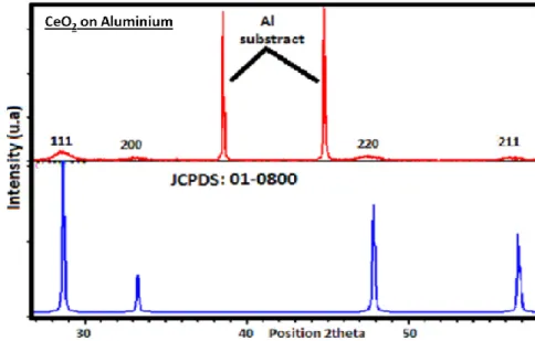
Pure ceria layer deposited on the aluminum substrate is characterized from structural side by XRD shaving in an angular range between 20 and 60 degrees. Figure 1 shows the diffraction pattern obtained with the crystalline phases that appear.
Figure 1: XRD patterns of the cerium oxide films elaborated at current density of 5 mA cm-1 for 120 min in 0.1 M Ce(NO3)3 is in agreement with the JCPDS card no 01-0800.
By analyzing the spectrum obtained with the software X’Pert HighScore, there is more than one part of the aluminum substrate and ceria; we have the presence of the phase Al2O3 which is formed by oxidation of the substrate. On the other hand, the rays of ceria are very broad, which shows that the grains electrodeposited are nanometric.
The calculated value of the crystallite size for this sample is between 30 nm. The following table shows the crystallite sizes for the different peaks.
Table 1: Crystallite size of CeO2 calculated by the Scherer equation
2θ (°) FWHM ( ° ) D (nm) 28.51 0.12 69.4 32.97 0.55 15.0 47.57 0.77 11.3 56.32 1.15 7.8 3.1.2 Microstructural analysis
2456
Figures 2.a and 2.b show that the thin layer of ceria contains cracks which are formed during heat treatment and are probably due to the departure of the organic phase or water molecules. The clusters vary in size and have the order of 100 microns.
Enlargement of clusters (Figures 2.c and 2.d) shows that they are composed of very small grains in the zone of the cerium oxide. The composition of the deposited films was confirmed by EDX (figure 2.f).
Figure 2: SEM images of CeO2 deposited on aluminum (a, b, c, d, e); (f): X-ray microanalysis spectrum of (b)
3.2 Bismuth oxide thin films
3.2.1 X-ray results
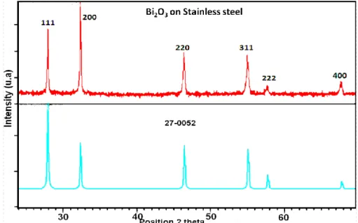
The thin films of bismuth oxide Bi2O3 synthesized were analyzed by XRD. The diffractogram obtained for this deposit is presented in the following figure:
J. Mater. Environ. Sci. 5 (S2) (2014) 135-139 EDE4 Hallaoui et al. ISSN: 2028-2508
CODEN: JMESCN
2457
Figure 3: XRD patterns of the bismuth oxide films elaborated at current density of 5 mA cm-1 for 120 min in 0.1 M Bi(NO3)3 is in agreement with the JCPDS card no 27-0052.
By analyzing the spectrum obtained with X’Pert HighScore software, it is clear that we synthesized the bismuth oxide δ-Bi2O3. We can see the occurrence of most of the lines corresponding to the bismuth oxide with nanometric size.
3.2.2 Microstructural analysis
To determine the morphology of the sample prepared, we conducted a study by Scanning Electron Microscopy. Figure 4 (a, b, c) shows the images obtained with secondary electrons.
2458
Figure 4.a represents an overview of the thin film and shows a fairly uniform distribution of bismuth oxide deposited. There is an homogenous morphology but with cracks between clusters of the studied material. In figure 4.b we observed clusters of micrometric size. However, by magnifying the image (figure 4.c) shows that the layer is in the form of small grains bonded shapes and sizes. EDX analysis confirms the synthesis of Bi2O3 (figure 4.d).
Conclusion
Pure Ceria and Bismuth thin films are synthesized with catalytic properties able to be integrated into devices of pollution control wastewater. The samples were prepared by electrodeposition on several substrates (Aluminium, Stainless steel and Copper) and these heat-treated at 400-450°C. Thin films obtained were characterized by X-ray diffraction (XRD) and scanning electron microscopy (SEM).
These analyses confirmed the deposition of catalytic phase pure CeO2 and δ-Bi2O3 thin films on an aluminum and stainless substrate.
Acknowledgment
Work published with the assistance provided under the agreement CNRST (Morocco) / CNRS (France).
References
1. Hamlaoui Y., Pedraza F, Remazeilles. C, Cohendoz S, Rébéré C, Tifouti. L, Creus J., J. Mater.Chem. Phys., 113(23) (2009) 650-657.
2. Zivkovic Lj. S., Lair V, Lupan O, Ringuedé A., Russ. J. Phys. Ch., 85(13) (2011)2358-2362.
3. Gujar T. P, Shinde. V. R, Lokhande. C. D, Han Sung-Hwan . J. Power Sources, 161 (2006) 1479–1485. 4. Laurent K, Wang G.Y, Tusseau-Nenez S, Leprince-Wang Y., Solid State Ionics 178 (2008)1735–1739.