HAL Id: hal-02406692
https://hal-amu.archives-ouvertes.fr/hal-02406692
Submitted on 12 Dec 2019
HAL is a multi-disciplinary open access
archive for the deposit and dissemination of
sci-entific research documents, whether they are
pub-lished or not. The documents may come from
teaching and research institutions in France or
abroad, or from public or private research centers.
L’archive ouverte pluridisciplinaire HAL, est
destinée au dépôt et à la diffusion de documents
scientifiques de niveau recherche, publiés ou non,
émanant des établissements d’enseignement et de
recherche français ou étrangers, des laboratoires
publics ou privés.
Boron Redistribution During Crystallization of
Phosphorus-Doped Amorphous Silicon
R. Simola, Dominique Mangelinck, A. Portavoce, J. Bernardini, P. Fornara
To cite this version:
R. Simola, Dominique Mangelinck, A. Portavoce, J. Bernardini, P. Fornara. Boron Redistribution
During Crystallization of Phosphorus-Doped Amorphous Silicon. AIP Conference Proceedings,
Amer-ican Institute of Physics, 2006, 866. �hal-02406692�
2
2
Boron Redistribution During Crystallization of Phosphorus-
Doped Amorphous Silicon
R. Simola
a), D. Mangelinck
a), A. Portavoce
a), J. Bernardini
a), P. Fornara
b)a) L2MP CNRS UMR 6137,case 142, Faculté des Sciences de Saint Jérôme,, 13397 Marseille cedex 13, France b) ST Microelectronics, 77 avenue Olivier Perroy,13790 Rousset, France
Abstract. The redistribution of boron has been studied during solid phase crystallization (SPC) of a homogeneous phosphorus-doped amorphous silicon layer deposited by low pressure chemical vapor deposition, for different thermal annealing. We show that for the lower temperature annealing (T = 586 °C, 1h) boron diffuses without changing the P profile, while for the higher temperature annealing (T = 800 °C, 3h), the initially homogeneous P profile is modified, showing two concentration peaks.
Keywords: Boron, Phosphorus, amorphous Silicon, Crystallization, Diffusion PACS: 78.40.Fy
INTRODUCTION
Dopant redistribution in silicon is of great importance in microelectronics. While boron diffusion has been extensively studied in crystalline silicon (c- Si), fewer studies exist concerning boron redistribution in poly-crystalline silicon [1-4] as well as in amorphous silicon [5-8]. In this work, we investigate the boron redistribution in a thin silicon film during a typical non volatile memory (NVM) process flow. In this process, the Si floating gate is first deposited on the Si oxide by low pressure chemical vapor deposition (LPCVD) as an amorphous homogeneously phosphorous-doped layer, and then implanted with boron. This layer crystallizes later in the process during the formation of the oxyde-nitride-oxyde (ONO) layer. The crystallization phenomenon is expected to greatly influence the redistribution of the dopants, and may lead to unusual variation of their concentration profiles versus the annealing time. For instance, it has been shown that both the nature of the dopant and its concentration can influence the silicon crystallization [9-10]. Furthermore, dopant diffusion depends on the crystalline state of the Si matrix, being faster in polycrystalline and amorphous Si than in monocrystalline Si.
EXPERIMENTAL
The samples were made of a 100 nm thick amorphous Si (a-Si) layer deposited by low pressure chemical vapor deposition (LPVCD) on a 12 nm thick
SiO2 layer, which has been thermally grown on
Si(001) substrates. The a-Si film was in-situ co- deposited with phosphorous at a temperature (T) of 530 °C, in order to obtain a homogeneous P
concentration of 7 × 10¹⁹ atoms / cm3 in the whole
layer. The a-Si film was then implanted with 11B+ ions,
with a beam energy of 7 keV and an ion fluence of 3.5
× 1015 atoms / cm2.
The samples were annealed under secondary
vacuum (pressure < 10–6 mbar) at temperatures
ranging from 585 to 800 °C for time between 1 and 50 hours. The temperature was measured using an in-situ thermocouple located at a few millimeters from the samples. Transmission electron microscopy (TEM)
measurements and X-ray Diffraction (XRD)
measurements have shown that all the samples were polycrystalline after these different thermal treatments. The dopant profiles were analyzed by secondary ion mass spectroscopy (SIMS). The B profiles were
measured using a 3 keV O + primary ion beam with an
incidence angle of 45° while the P profiles were acquired under oxygen atmosphere (oxygen leak)
using a 3 keV O + primary ion beam with an incident
angle of 25.2°.
Complementary experiments were performed in order to estimate the crystallization time (time which
C on ce nt ra tio n (c m -3 )
is needed to completely crystallize the a-Si layer at a given temperature). In-situ XRD measurements were performed on a-Si undoped, phosphorus-doped and boron-doped layers made following the same process as previously described. During isothermal annealing
at T = 565 °C under vacuum (p < 10–4 mbar), the
variations of the (111)Si X-ray peak intensity was recorded versus time, in the classical Bragg-Brentano geometry. The temperature was monitored using a thermocouple in contact with the surface of the samples.
RESULTS AND DISCUSSION
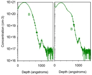
The boron concentration profiles measured before and after a low temperature thermal annealing (1h at 585 °C) are shown in Fig. 1. Despite an annealing at low temperature, a non negligible part the B atoms did diffuse and an additional shoulder appear on the profile.
1E+21 1E+20 1E+19
It is important to notice that for these experiments the concentration of boron in the as-implanted sample is notably higher than the boron solubility limit in
monocrystalline Si (~ 4 × 1017 cm–3 at 600 °C [12]).
Thus the fact that a part of the B atoms did not diffuse can be explained considering that during the annealing the immobile atoms formed boron-interstitial-clusters (BICs), whose properties have been the object of theoretical [13-15] and experimental [16-20] studies.
Fig. 1 shows that boron atoms which have diffused during the thermal treatment correspond to a
concentration lower than 2 × 1020 cm–3, which is
higher than the common solubility limit of B in c-Si at 600 °C. This higher value can be understood considering that atoms could have diffused while the layer was still amorphous. In this case the solubility limit of B is expected being higher than in c-Si (a-Si has a lower density than c-Si [21]) and is not precisely known as it may depend on the nature of the amorphous layer. Also, it has been shown that in the case of implanted pre-amorphized Si layer the solubility of B can be greatly increased after solid
phase epitaxial crystallization ( 3.5 × 1020 cm–3 in the
temperature range T = 800-1000 °C [22] and up to 2 ×
1020 cm–3 in the low-temperatures range T=500-600°C
[7] ). The same mechanism can take place in our experiments. 1E+18 1E+17 1E+16 0 1000 Depth (angstroms) 0 1000 Depth (angstroms) 1E+21 1E+20 1E+19 1E+18
FIGURE 1: Boron profile measured by SIMS, before thermal annealing (left) and after T = 585 °C 1h annealing (right).
One can clearly observe on Fig. 1 that this shoulder
located in the region between 50 nm (CBB = 2 × 10
20
cm–3) and 70 nm (C
BB = 8.5 × 10
19 cm–3) is followed
by an abrupt slope which ends at a depth of ~ 94 nm
1E+17 1E+16 0 1000 Depth (angstroms) 0 1000 Depth (angstroms) (CBB = 4 × 10
17 cm–3). The peak at a depth of ~ 100
nm, located in the SiO2 layer zone, is certainly a SIMS
artifact due the so-called matrix effect [11], which originates here from a higher ionization rate of B
atoms in the SiO2 matrix compared to the Si matrix.
FIGURE 2: Phosphorus profile measured by SIMS, before thermal annealing (left) and after T = 585 °C 1h annealing (right).
The width of the extra-shoulder observed on the SIMS profile measured after annealing can be considered as the diffusion length of the B atoms
B B P P C on ce n tr at io n (c m -3 )
during the treatment. It is about 20 nm. This distance is somewhat greater than the one expected for boron diffusion in polycrystalline Si (poly-Si), as according to [2] this distance should be only of ~ 7 nm for our annealing conditions. This may be explained by a faster diffusion of boron in a-Si.
Furthermore, the abrupt slope observed after the shoulder (depth greater than 70 nm) cannot be simulated with a diffusion model using a constant diffusion coefficient (even if the presence of boron clusters is considered). Different phenomena that could explain this abrupt slope include a concentration dependence of the boron diffusion coefficient and/or the influence of the mobile interface between the amorphous and the crystalline parts of the Si layer during the crystallization.
Figure 2 shows that the phosphorus profile is found unchanged after the lower temperature annealing (T = 585 °C, 1h). This is what is reasonably expected in the case of a homogeneous material, as the SIMS profile of phosphorus does not present any concentration gradient. Neither the presence of boron, nor the crystallization is thus found having a significant effect on the phosphorus distribution.
As already cited, at sufficient high temperatures crystallization of doped a-Si takes place relatively quickly. Normalized (111)Si X-ray diffraction peaks (2=28.4°) for undoped a-Si (250 nm-thick), phosphorus-doped a-Si (150 nm-thick) and boron implanted a-Si (250 nm-thick) as a function of annealing time are shown in Fig. 3 . All the samples where annealed at T=565 °C.
1
In all three cases, the intensity peak does not start to increase immediately; it takes some time, a latent time, for crystallization to start. This latent time is maximum for undoped a-Si and minimum for the phosphorus- doped a-Si film. The phosphorus doped a-Si sample is the fastest to crystallize; total time for crystallization is about 360 minutes at T=565 °C. At higher temperatures, crystallization time should be much shorter because of the exponential dependence of crystallization rate on temperature. Through these measurements we were able to: i) confirm that boron and phosphorus enhance crystallization; ii) set a lower bound for crystallization time for all the experiments that we have performed.
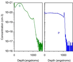
Figure 4 shows the boron (left) and the phosphorus (right) profiles measured after annealing at 650 °C for 50 hours. In contrast with the previous annealing (T = 585 °C, 1h) diffusion in poly-Si cannot be neglected anymore [2]. As the Si film is found being polycrystalline after a thermal treatment at 585°C for 1 hour, it is reasonable to consider that at 650 °C for 50 hours the crystallization is faster (diffusion in the a-Si is shorter), and thus boron atoms diffuse in a poly-Si matrix during at least 49 hours. The boron profile, at a depth below 70 nm is found to be similar to the one obtained during the lower temperature annealing.
1E+21 1E+20 1E+19 1E+18 0,5 1E+17 1E+16 0 1000 Depth (angstroms) 0 1000 Depth (angstroms) 0 0 600 1200 time (minutes)
FIGURE 3: XRD normalized peaks for non doped (circle), phosphorus doped (triangle) and boron doped (square) a-Si films, as a function of annealing time at T=565 °C.
FIGURE 4: Boron (left) and phosphorus (right) profiles after T = 650 °C 50h thermal annealing.
The significant changes in the boron profile, compared to the boron profile obtained after annealing at 585 °C for 1 hour, start from a depth of 70 nm with
a concentration about CBB = 1 × 10 20 cm–3. We B P In te ns ity ( n o rm a liz e d ) C on ce nt ra tio n (c m -3 )
.
B
conclude that the left part of the profile (depth below 70 nm) is mainly due to the boron redistribution before and during crystallization, while for greater depth the concentration profile of boron results from the diffusion of atoms in poly-Si. Boron solubility limit in
phosphorus-doped poly-Si seems thus to be 1×10²⁰
ACKNOWLEDGMENTS
The authors would like to thank K. Hoummada for the help concerning the XRD measurements.
REFERENCES
cm–3 consistent with the previous study [13]. The
right-hand phosphorus profile in Fig. 4, shows an almost constant concentration after the annealing, with small variations at depth around 33 nm and 70 nm where little local maxima appeared.
High-temperature crystallization annealing
(T=800°C, 5h) results are shown in Fig. 5 for boron (left) and phosphorus (right). Boron profile is quite flat
between 75 nm and 94 nm (CB=1.2×1020 cm–3 and
9.3×1019 cm–3 respectively) due to boron diffusion in
polycrystalline silicon. The rest of the profile, namely for depth below 70 nm, is similar to the one obtained after low-temperature annealing (T=585°C, 1h) despite a significant change in the 30 nm peak which concentration diminished and reached the value of
6×1020 cm–3 We conclude that at T=800°C 5h, boron
diffusion length in polycrystalline is about 20 nm. Atomic Force Microscopy measurements (not shown in this paper) yield an average diameter of 40 nm for the grains. Phosphorus profile displays two concentration peaks at 30 nm and 70 nm; since concentration profile is constant before annealing, these peaks are certainly due to boron-phosphorus interactions; such interaction may include electrical and/or chemical ones.
1E+21 1E+20 1E+19 1E+18 1E+17 1E+16
1. T.I. Kamins, J. Manoliu, R.N. Tucker, Tucker, J. Appl. Phys. 43, 83 (1972)
2. K.Sakamoto, K. Nishi, T. Yamaji, T. Miyoshi and S. Ushio, J. Electrochem. Soc. 132, 2457-2462 (1985) 3. A. Merabet, C. Gontrand, Mat. Science and Eng. B102,
257-261 (2003)
4. B. Semmache, A. Merabet, C. Gontrand, A. Laugier, Mat. Science and Engin. B38, 41 (1996)
5. J. M. Jacques, L.S. Robertson, K.S. Jones, Appl. Phys. Lett. 82, 3469-3471 (2003)
6. R. Duffy, V.C. Venezia, A. Heringa, T.W.T. Husken, M.J.P. Hopstaken, N.E.B Cowern, P.B. Griffin, C.C. Wang, Appl. Phys. Lett. 82, 3647-3649 (2003)
7. R. Duffy, V.C. Venezia, A. Heringa, B.J. Pawlak, M.J.P. Hopstaken, G.C.J Maas,Y. Tamminga, T. Dao, F. Roozeboom, L. Pelaz, Appl. Phys. Lett. 84, 4283-4285 (2004)
8. V.C. Venezia, R. Duffy, L. Pelaz, M.J.P Hopstaken, G.C.J. Maas, T. Dao, Y. Tamminga, P. Graat, Mat. Science and Engin. B124-125, 245-248 (2005) 9. R. Bisaro, J. Magarino, K. Zellama, S. Squelard, P.
Germain, J.F. Morhange, Phys. Rev. B 31, 3568-3575 (1985)
10. H-C. Cheng, F-S. Wang, Y-F. Huang, C-Y. Huang, J. Electrochem. Soc.142, 3574-3578 (1995)
11. V. R. Deline, William Katz, C. A. Evans, Jr., and Peter Williams, J. Appl. Phys. 33, 832 (1978)
12. P. Pichler, Mat. Res. Soc. Symp. Proc. 717, 103 (2002) 13. L. Pelaz, M. Jaraiz, G. H. Gilmer, H.-J. Gossmann, C.S.
Rafferty, D. J. Eaglesham, and J. M. Poate, Appl. Phys. Lett. 70, 2285 (1997)
14. X.-Y. Liu, W. Windl, and M. P. Masquelier, Appl. Phys. Lett. 77, 2018 (2000)
15. P. Alippi, P. Ruggerone, L. Colombo, Phys. Rev. B 69, 125205 (2004)
16. G. Mannino, N. E. B. Cowern, F. Roozeboom, J. G. M. van Berkum, Appl. Phys. Lett. 76, 855 (2000)
17. A. D. Lilak, M. E. Law, L. Radic, K. S. Jones, M. Clark, Appl. Phys. Lett. 81, 2244 (2002)
18. S. Mirabella, E. Bruno, F. Priolo, D. De Salvador, E. Napolitani, A. V. Drigi, A. Carnera, Appl. Phys. Lett. 83, 680 (2003)
19. A. M. Piro, L. Romano, S. Mirabella, M. G. Grimaldi, Appl. Phys. Lett. 86, 81906 (2005)
0 1000
Depth (angstroms)
0 1000
Depth (angstroms)
20. L. Romano, A. M. Piro, S. Mirabella, M. G. Grimaldi, E. Rimini, Appl. Phys. Lett. 87, 201905 (2005)
21. J.S. Custer, M.O. Thompson, D.C. Jacobson, J.M. Poate, S. Roorda, W.C. Sinke, F. Spaepen, Appl. Phys. Lett. 64, FIGURE 5: Boron (left) and phosphorus (right) profiles
after T=800°C 5h thermal annealing
437-439 (1994)
22. S. Solmi, E. Landi, F.Baruffaldi, J. Appl. Phys. 68, 3250 (1990) B P C o n ce n tr a tio n (c m -3 )