M
AN
US
CR
IP
T
AC
CE
PT
ED
1Random angle grain boundary formation and evolution dynamics
during Si directional solidification
M.G. Tsoutsouva1, G. Stokkan2, G. Regula3, B. Ryningen2, T. Riberi – Béridot3, G. Reinhart3, N. Mangelinck-Noël3
1
Dept. of Physics, Norwegian University Science and Technology, 7491 Trondheim, Norway,
2
SINTEF Industry, Trondheim, Norway,
3
Aix Marseille Univ, Université de Toulon, CNRS, IM2NP, Marseille, France
Abstract
The growth of multicrystalline silicon and the formation of a random angle grain boundary, as well as the dislocation generation and expansion is observed dynamically
in situ, by Synchrotron X-ray imaging techniques. The focus is kept on a random angle
grain boundary since its behavior is particularly important to better understand the HP mc-Si (High Performance Multi-crystalline Silicon) photovoltaic properties. Due to the process conditions and to the grain competition that occurs during the solidification, a facetted {111} /facetted {111} groove is formed by this random angle grain boundary at the solid/liquid interface. It is shown how the shape of the solid/liquid interface allows the change of the preferential {111} growth facet and affects the grain boundary propagation direction. In one of the groove configurations, the two adjacent {111}
M
AN
US
CR
IP
T
AC
CE
PT
ED
2facets do not have the same growth velocity and as a consequence the corresponding grain boundary does not follow the bisector of the angle between the two facets. Indeed, the direction of the grain boundary is determined by the growth velocities of the facets which control the grain competition. Moreover, under these experimental conditions a clear relationship is observed between the existence of random angle grain boundaries and the local generation of dislocations as well as their expansion. By comparison, dislocation emission is not observed at the level of Σ3 {111} grain boundaries.
Keywords: X-ray radiography, Bragg diffraction imaging (topography), crystalline defects, dislocations, grain growth, grain competition
1 Introduction
Unlike the traditional mc-Si process characterized by large grains and predominant electrically-inactive twin boundaries, the crystal growth of high-performance multi-crystalline silicon (HP mc-Si) by directional solidification is nucleated on uniform small grains, resulting in a material with a high fraction of random angle grain boundaries (RAGBs). The HP mc-Si process concept and the first results were presented in the 5th International Workshop on Crystal Growth Technology in June of 2011 by Professor C. W. Lan [1]. The ingots solidified with this technique present not only a better uniformity and a higher production yield but also an improved material quality for photovoltaic applications. Since 2011, different approaches have been proposed to obtain such a grain structure [2–6]. As a result, the average efficiency
M
AN
US
CR
IP
T
AC
CE
PT
ED
3of HP mc-Si solar cells in production increased from 16.6% in 2011 to 18.5% or beyond in 2016 [7].
The lifetime of HP mc-Si is in general uniform and higher than what was achieved for the traditional mc-Si due to the limited influence of the harmful dislocation clusters. Indeed, the areas with high dislocation density are confined in the small grains and the propagation of dislocation clusters from the bottom to the top seems to be blocked by the presence of RAGBs [7]. Trying to understand the involved mechanism leading to the improved performance of the HP mc-Si, different theories have been proposed in relation to grain growth, dislocation generation, multiplication and interaction with grain boundaries.
It is believed that the uniform and small-grained structure reduces the stress concentration at the initial stage of solidification and thus the initial dislocation generation. It has also been suggested, however without clear evidence, that the presence of RAGBs can additionally relax stresses through a slip mechanism at high temperatures [6,8]. It is expected that since the global stress is reduced and that the dislocation sources are less abundant, the dislocation multiplication mechanisms are less active. Stokkan et al. [9] assumed that RAGBs contain heavily mis-reconstructed bonds so that when the predominantly vertical clusters of lattice dislocations interact with such boundaries the bonds can be more easily rearranged while the grain boundary energy
M
AN
US
CR
IP
T
AC
CE
PT
ED
4changes very little. Hence, the boundaries correspond to more ductile areas (than the grain themselves) where the dislocations can be trapped. Whatever mechanism, due to the existence of a high length fraction of RAGBs in HP mc-Si, where dislocations are prevented to move across, the development of large dislocation clusters during growth is limited. Furthermore, from recent investigations, it was shown that the recombination activity of the grain boundaries in HP mc-Si wafers is much lower than in the conventional mc-Si but the reason of this observation still remains unknown [10, 11]. Apparently, apart from the grain size, the crystallographic relationship and the lattice misfit between two adjacent grains have a significant impact on the dislocation movement and thus, on the minority carrier lifetime in the area of the grain boundary [12].
The detailed mechanisms of grain competition and selection that lead to grain boundary formation as well as dislocation generation, multiplication and interaction with grain boundaries (nucleation and/or termination) are not well understood. A better knowledge of these mechanisms is a prerequisite for controlling the final structure and is thus vital to be able to achieve the desired crystal properties. However, it is difficult to get an understanding of the phenomena that occur during the solidification process, by ex situ characterization of the cooled down crystal. There is no information left about
M
AN
US
CR
IP
T
AC
CE
PT
ED
5the morphology of the solid/liquid interface and of the grain competition dynamics during growth.
In the present work, our approach to tackle this challenge is to observe dynamically the directional solidification of silicon, by a combination of X-ray diffraction imaging techniques: X-ray radiography and Bragg diffraction imaging (Topography). By X-ray radiography it is possible to follow the morphology of the solid/liquid interface which gives information about the growth kinetics, whereas Bragg diffraction imaging allows following in situ the evolution of the extended defect formation. The formation of a RAGB and its interaction with extended defects are studied in particular since RAGBs have been identified as one of the main features leading to the improved PV performance of the HP mc-Si ingots.
2 Experimental
The directional solidification experiment is carried out in a dedicated installation named GaTSBI (Growth at high Temperature observed by X-ray Synchrotron Beam Imaging), which is installed at the European Synchrotron Radiation Facility (ESRF). GaTSBI is composed of a Bridgman-type high temperature furnace equipped with two resistive heating elements (top and bottom) and is coupled with in situ X-ray imaging techniques. X – ray radiography is performed using a specific CCD camera developed at
M
AN
US
CR
IP
T
AC
CE
PT
ED
6the ESRF named FReLoN (Fast Readout Low- Noise) with 2048×2048 image pixel size. An optic giving 5.8 µm pixel size and 11.9 × 11.9 mm2 field of view is used. Alternately during the same solidification experiment, X-ray Bragg diffracted images (of Von Laue patters), corresponding to different {hkl} diffracting planes, are regularly recorded on X – ray sensitive films (AGFA Structurix D3-SC, 17.6×12.5 cm2) positioned at a distance of 300 mm from the sample. The Bragg diffraction imaging technique is sensitive to long range distortion fields and / or strain fields associated with crystal deformation. Indeed, the distortion fields affect the diffracted intensity, so that a contrast (non – homogeneous intensity distribution) is created in the recorded images. As a consequence, defect-induced strain in general and in particular, dislocations are visible due to the deformation they cause to the crystalline network in their vicinity. Due to the small beam divergence and to its large size, the whole width of the sample is illuminated and the recorded diffraction spots contain information concerning the level of crystal perfection and/or deformation including dislocations. It is worth mentioning
that in the diffracted images, contrast variations can also be due to different Bragg angles (superimposition or separation) of two diffracted zones with a different orientation. This case is neither observed nor discussed in the present work. A more detailed description of the experimental conditions, the imaging techniques, image processing and the previously obtained results can be found elsewhere [13–15].
M
AN
US
CR
IP
T
AC
CE
PT
ED
7In the present work, the initial monocrystalline Si sample is appropriately cut (38 mm × 5.8 mm × 0.3 mm) from a double side mechano – chemically polished intrinsic (resistivity beyond 5000 Ωcm) FZ wafer 50.8 mm, {110} in surface orientation provided by SIL’TRONIX Silicon Technologies. After the cutting process, the sample is chemically polished in order to smoothen the damaged areas due to the cutting step: first an HF bath followed by a CP4 polishing, with a newly fabricated solution at room temperature during 3 min. Solidification experiments are performed under dynamic vacuum (~10-6mbar) while the sample is housed in between tow pyrolytic BN plates, in a cavity with dimensions: length 40.0 mm, width 6.0 mm and depth 0.3 mm.
The sample is heated by applying the same temperature at the bottom and top heating resistances of the furnace up to 1373 K. Then, a temperature gradient of 30 K/cm is imposed between the two heating resistances until partial directional melting from top to bottom is achieved. After the stabilization of the solid/liquid interface, a cooling rate of -1 K/min is applied on both heaters to start a directional solidification from bottom to top, while recording X-ray images of both types.
After solidification, the sample is analyzed by electron backscatter diffraction (EBSD) on a SEM JSM840 using 15 µm step size and on a FEG-SEM, Zeiss Ultra, 55 Limited Edition using 3 µm step size for selected regions. In order to depict the obtained crystallographic orientations of the grains in the sample, inverse pole figures (IPF) maps
M
AN
US
CR
IP
T
AC
CE
PT
ED
8are generated with respect to the three main directions relatively to the sample: perpendicular to the sample surface (x), transverse (y) and along the growth direction (z). Coincidence site lattice maps (CSL) show CSL boundaries as defined by the Brandon criteria [16].
3 Experimental results
As already mentioned in the introduction, the purpose of the present work is the investigation of the growth kinetics and of the extended defect generation related to the formation and evolution of a random angle grain boundary (RAGB) during the solidification process.
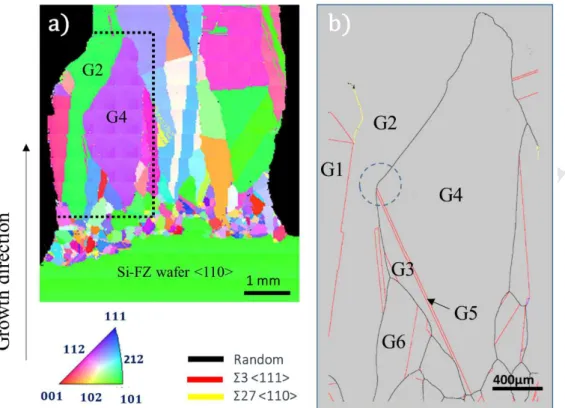
Figure 1a presents the inverse pole figure map (IPF) along the direction perpendicular to the sample surface obtained by EBSD of part of the solidified crystal. The CSL EBSD map, recorded at higher resolution (3 µm step size) in the area limited by the dotted rectangle (Figure 1b), reveals the details of the grain structure and of the grain boundary characters.
M
AN
US
CR
IP
T
AC
CE
PT
ED
9Figure 1: EBSD measurements (Gi are the names of different grains, 1<Gi<6); a) Inverse pole figure map along the direction perpendicular to the sample surface, using 15 µm lateral step size and b) coincidence site lattice map (CSL) in the area limited by the dotted rectangle in Figure 1a, 3 µm lateral step size. The dotted circle corresponds to the change of the RAGB direction, when G1 meets G4, as growth proceeds.
In the following, the experimental results and discussion focus on the area where a RAGB is formed as the result of the grain competition between Grain 2/Grain 3 and Grain 2/Grain 4 (the respective grains are marked as G2, G3 and G4 in Figure 1). The complete EBSD information allows to conclude that grains G3 and G4 have exactly the same crystallographic orientation (they appear in purple color in Figure 1a) and are separated between them by the diagonal twin crystal G5 that can be hardly distinguished
M
AN
US
CR
IP
T
AC
CE
PT
ED
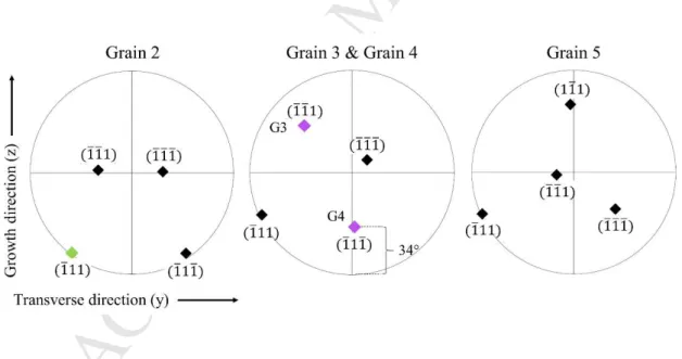
10in Figure 1a, because of the lower resolution, but which is clearly revealed in Figure 1b. During growth, the grains G3 and G4 enter in competition with the grain G2 forming RAGBs that propagate along different growth directions. On the one hand, in the case of G2/G3, the RAGB formed is almost vertical and follows the growth direction. On the other hand, shortly after the intersection with the diagonal double twin G5, when G2/G4 meet each other, the RAGB growth direction changes remarkably (dashed circle in Figure 1b). Indeed, it turn towards the right with reference to the growth direction, looking along the x direction. In order to investigate this behavior, the facet growth kinetics as well as the competition mechanism between G2, G3 and G4 are further analyzed. For that purpose, the stereographic projections of the {111} poles corresponding to the plane view normal to the sample surface direction (axis x) are presented in Figure 2.
Figure 2: Stereographic projections of the {111} poles of grains G2, G3, G4 and G5, the pole axis (x) being along the direction perpendicular to the sample surface. The {111} poles marked with the green and purple diamond symbols correspond to the
M
AN
US
CR
IP
T
AC
CE
PT
ED
11facets that preferentially drive the G2 and G3/G4 growth during the solidification process respectively.
The morphology of the solid/liquid interface at the level of the RAGB formation between G2/G3 and G2/G4 is revealed in live by X-ray radiography and representative images are given in Figure 3a and b. The radiograph in Figure 3a corresponds to the instant t = to + 75s (to corresponding to the beginning of the solidification process),
before the position indicated by the dotted circle in Figure 1b while the radiograph in Figure 3b corresponds to the instant t = to + 194s, after the position indicated by the
M
AN
US
CR
IP
T
AC
CE
PT
ED
12Figure 3: X-ray radiography zoomed image at the level of the facetted/facetted grain boundary groove formed at the solid/liquid interface, as the result of the grain competition between a) G2/G3 (t = t0 + 75 s) and b) G2/G4 (t = t0 + 194 s) respectively.
Graphical add – ins are superimposed on the images (ii) and (iii) for a better understanding of the discussion that follows. to corresponds tothe beginning of the
solidification process.
The images are the result of a pixel by pixel division of two successive raw images. The image treatment is required to increase the contrast and reveal the solidification front and allows the study of the dynamical interface and facet evolution [13]. The solid appears in white (less dense) and the liquid in grey (denser) and since the image is a division of successive images, the white contrast means that a liquid layer in the previous image has solidified in the following image.
Both radiographs show that the encounter of grains G2/G3 and G2/G4 creates a facetted/facetted groove at the solid/liquid interface but of different shape. The traces of the {111} corresponding to the facets seen in projection at the solid/liquid interface are indicated in Figure 3a (ii), (iii), b (ii), (iii). The inclinations of the {111} facets are in agreement with the respective poles on the stereographic projections for both grains (Figure 2). The growth of G2 is driven by its 111 facet in both grain boundary
M
AN
US
CR
IP
T
AC
CE
PT
ED
13direction (edge zone) and 36° inclined by the growth direction. Even if G3 and G4 have exactly the same crystallographic orientation, their growth is driven by different {111} facets at the level of the grain boundary groove with G2. On the one hand, G3 grows
along the 111 facet which is 66° inclined by the sample surface direction and 45°
inclined by the growth direction (Figure 2). On the other hand, G4 grows along the
111 facet that is almost perpendicular to the growth direction and 56° inclined by the
sample surface direction (34° by the edge zone). The trace of the bisector of the angle between the two facets is also shown with a dashed yellow arrow in the same radiographs. It must be noted that the actual bisector of the groove facets is slightly different from the apparent bisector of the traces in the figure due to the inclination of
the G3 111 and G4 111 facets relatively to the plane of the figure. The actual
bisector and its trace is found by the use of a Wulff plot on the two pole figures. In Figure 3, the black arrow shows the actual mesoscopic direction of the formed RAGB and the blue dotted line is an estimation of the isotherm shape.
The RAGB formed as the result of the grain competition between G2 and G3 (Figure 3a) follows the bisector of the angle between the two facets ( 111 and 111 )
as proposed by the model of Duffar et al. [17], when both {111} facets of the facetted/facetted groove grow at the same rate. On the contrary, when G2 and G4 enter in competition, the formed RAGB does not follow the bisector of the angle between the
M
AN
US
CR
IP
T
AC
CE
PT
ED
14two facets (Figure 3b) denoting that the 111 and 111 facets of the groove grow
with different rates.
To confirm this statement, the growth velocities normal to the facet planes in the case of G2/G3 and G2/G4 grain competition are measured from the radiography images recorded during the solidification. Figure 4 shows the displacement of the normal to the facets as a function of time as growth proceed and the slope of the trend line corresponds to the average facet growth velocities. As illustrated in Figure 4a, in the case of G2/G3 grain competition the average facet growth velocities of G2 111 and
G3 111 are comparable ( = 2.29 ± 0.09 × 10 / and = 2.21 ±
0.05 × 10 / ). (a) (b) = . ± . × ! "/# $= . ± . % × ! "/# Zone I: = . $ ± . × ! "/# &= '. $( ± . × ! "/#
Zone II: = . $& ± . % × % "/# &= . ! ± . × %"/#
M
AN
US
CR
IP
T
AC
CE
PT
ED
15Figure 4: Displacement of the normal to the a) G2/G3 and b) G2/G4 {111} facets as a function of time, during the solidification process as measured using the time-resolved X-ray radiography images. The slopes of the trend lines corresponds to the velocity normal to the facet. The error of the measurement is within the size of the symbols.
The respective curves for G2 111 and G4 111 are presented in Figure 4b.
For both grains, the measured points can be grouped in two zones, zone I and zone II, in which G2 as well as G4 accelerate. However, in both zones I and II, G2 grows faster than G4 implying that the growth kinetics of the two grains are not identical. The average measured growth velocity of the solid/liquid interface in this experiment is
) = 2.10 ± 0.05 × 10 *m/s (measured from the dynamic radiography images) and
is always higher than the {111} facet growth rate as expected due to the slower kinetics of {111} facets. The local temperature gradient G is calculated with the equation
- = ./ ) where . = 1.66 × 10 K/s is the cooling rate applied to both resistive
heaters to start solidification during the experiment: - = 7.9 ± 0.4 × 10 K/m [18].
White beam X-ray Bragg diffraction images are recorded in situ during the same solidification experiment and representative images of the G2, G3 and G4 grain growth evolution are shown in Figure 5a and b. Figure 5a (ii) and b (ii) show the diffraction images of the grains when G2 grows in competition with its neighbor G3, while Figure
M
AN
US
CR
IP
T
AC
CE
PT
ED
165a (iii) and b (iii) correspond to an instant just after G2 enters in contact with G4, instead of G3 (position of the dotted circle in Figure 1b). G3 and G4 diffract together in the same diffraction spot (Figure 5b) because they have the same crystallographic orientation [19]. Equal-thickness fringes, related to Pendellösung fringes are clearly observed in the crystal. This contrast is attributed to the dynamical diffraction effect inside the crystal matrix and indicates a high-level of crystalline quality (less than 102 cm-2 dislocation density [20]). Thus, as long as these fringes are observed, G2 and G4 grow as high quality crystals.
a) Grain G2
M
AN
US
CR
IP
T
AC
CE
PT
ED
17 to + 46 s to + 104 s to + 159 s to + 176 s to + 218 s to + 268 sFigure 5: White beam X-ray Bragg diffraction images taken during the solidification process a) G2; b) G3 and G4 grain growth. to corresponds to the beginning of
solidification.
However, the intensity distribution is not homogeneous and some areas are significantly darker than others. As explained in the experimental section, in Bragg diffraction images, dark areas correspond to highly deformed/strained areas and the dislocation density is estimated to be ≥ 106 cm-2. At the instant when G2 and G4 enter into contact, the formation of the inclined RAGB is accompanied with the generation and emission of dislocations in both adjacent grains that become more and more strained as growth proceeds (Figure 5 (iii) to (vi)). In general, there is a strong correlation between the highly strained areas and the grain boundary types (Figure 1b) formed due to the competition between G1 - G6 as will be discussed in further details in the following section.
M
AN
US
CR
IP
T
AC
CE
PT
ED
18 4 Discussion4.1 Facet growth kinetics and grain competition mechanism
Solidification started from the nucleation on numerous randomly oriented grains that can be seen in Figure 1. G1 – G6 grains resulted from the competition between the initially growing grains. Depending on the grain orientation and on the direction of the resulting grain boundary relatively to the growth direction, some of the grains expand during the solidification process while others lose the competition with the adjacent grains and disappear [21]. In the experiment described here, G3 and G5 lose the competition and as a consequence G2 and G4 enter into contact as growth proceeds (dotted circle in Figure 1b).
Under the present experimental conditions, independently from the macroscopic growth directions of G2, G3 and G4, the growth is bounded by the slowest growing planes and a clear {111} facet appearance at the solid/liquid interface can be seen for all grains in the radiography (Figure 3a, b) and Bragg diffraction images (Figure 5a, b).
The radiograph reveals that when G2 and G3 meet, a facetted/facetted groove is formed at the solid/ liquid interface at the level of their common RAGB. Such a configuration has been theoretically modelled by Duffar and Nadri [22] and experimentally shown previously using the GaTSBI device [23]. In the model case of a
M
AN
US
CR
IP
T
AC
CE
PT
ED
19facetted/ facetted groove, the undercooling at the bottom of the groove is maximum and identical for both {111} facets. Therefore, both facets have the same growth velocity and as a consequence, the direction of the grain boundary formed follows the bisector of the angle between both facets [22]. As showed experimentally in ref. [15], this is true
when the two adjacent grains have no specific CSL crystallographic relation. If they do have, the grain boundary preferentially follows the common plane in order to minimize the energy of the formed grain boundary. Such a plane could be for example the {111} or {112} if the adjacent grains have a Σ3 CSL relation, the {122} or {114} if they have a Σ9 CSL relation. In the present experiment, this is the case of the two Σ3 {111} grain boundaries that are formed between both G3/G5 and G4/G5 when they compete (Figure 1b).
At first, G3 is in competition with both G2 and the double twin grain G5 in between G3 and G4. According to the radio images (Figure 3a) and trace of the random angle grain boundary (Figure 1b), G3 slowly expands at the detriment of G2 but ultimately loses competition with G5. For a very short time, a RAGB is established between G2 and G5. Finally, G5 loses competition against G2 and a new RAGB is formed at the encounter of G2 and G4. Even if G3 and G4 have the same crystallographic orientation, G4 is a grain that nucleated independently from G4 and its growth is driven by a different {111} facet as can be seen in both radiography (Figure
M
AN
US
CR
IP
T
AC
CE
PT
ED
203a, b) and Bragg diffraction images in Figure 5b (i), where G3 grows with the diagonal
111 and in Figure 5b (ii) where G4 grows with the horizontal 111 facet at the level
of the grain boundary groove. Thus, the groove configuration changes from the G3 to G4 interaction with G2 as illustrated in Figure 3a and Figure 3b. Such a growth {111} facet change probability for grains with the same crystallographic orientation has been previously theoretically proposed by Nadri et al. [21]. This event could be the result of the isotherm shape change with time according to Nadri's theory. As presented in Figure 3a (iii), b (iii), the isotherm shape is almost horizontal during the G2/G3 competition resulting in a flatter solid-liquid interface but the isotherm (derived from the average solid-liquid interface shape) is concave when G2 and G4 compete with each other. This isotherm change could be due to the sudden change (narrowing) of the sample lateral size as can be seen on the radiography image in Figure 3b. Thus G4 which has the same
orientation as G3 cannot grow with the same diagonal 111 facet since it hardly faces
the solid-liquid interface. Grain growth driven by facets, resulting the creation of a grain boundary that follows as close as possible the direction of the temperature
gradient, is always favored. In the present case, this facet is the G4 111 which is the
horizontal facet that guides the growth of G4 from the beginning of its nucleation (Figure 5b). As a consequence, the random angle grain boundary direction between G2 and G3 is different from the one between G2 and G4. A simplified 2D model that could
M
AN
US
CR
IP
T
AC
CE
PT
ED
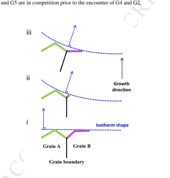
21explain the {111} growth facet change, during the solidification of two grains that are in competition, due to the change of the isotherm shape is presented in Figure 6.
Moreover, it is also possible that the presence of the double diagonal twin grain G5 contributes to the selection of the {111} growth facet of G4 at the RAGB groove since G4 and G5 are in competition prior to the encounter of G4 and G2.
Figure 6: A simplified 2D model that illustrates and explains the growth facet {111} change mechanism during the solidification process, due to the change of the isotherm shape. i) The isotherm and thus the overall solid/liquid interface shape is horizontal, a V-shape groove is formed, the grain boundary follows the bisector of the
M
AN
US
CR
IP
T
AC
CE
PT
ED
22groove angle and grows parallel to the normal to the isotherm (direction of the temperature gradient) ii) The isotherm becomes concave and thus the diagonal facet of Grain B (respective 2 2 facet of G3) faces much less the solid/liquid interface.
In addition the direction of the grain boundary formed deviates from the direction of the temperature gradient. Such a configuration is not favorable. iii) The isotherm shape is concave and another facet that faces the solid/liquid interface is selected to
guide the growth. In the present case this is the horizontal 2 2 facet of G4. As a consequence the growth direction of the grain boundary is also different and parallel to the temperature gradient.
During the concomitant growth of G2 and G4, the RAGB does not follow the bisector of the groove, which is illustrated with the yellow dotted line in Figure 3b. Indeed, the actual direction of the RAGB is indicated with a black arrow in the same figure and it is inclined by ~ 17 ± 3° to the bisector of the groove angle. It is
important to note that this is not in contradiction with the model of Duffar and Nadri [22] in which the starting hypothesis is that both facets grow at the same rate. In this particular case, both grain boundary groove {111} facets do not share the same growth rate, as can be seen in Figure 4. Two possible explanations for the fact that G4 grows faster that G3 are discussed in the following.
M
AN
US
CR
IP
T
AC
CE
PT
ED
231. A radial temperature gradient causing an asymmetric thermal field in the grain boundary groove.
The temperature distribution in the sample has a strong impact on the crystal growth velocity, the interface shape and the grain boundary formation during the crystal growth process. Similarly to what has been presented by Lian et. al [24], in our experimental installation the shape of the crystal/melt interface at the level of G2/G4 grain competition is curved maybe due to the sample shape change. This leads to the creation of a radial temperature gradient that causes a curvature of the isotherm. Since the two facets meet at the triple junction of the two grains they should have the same undercooling temperature and thus grow with the same velocity. However, the inclination of the two {111} facets is not identical relatively to the isotherm shape as illustrated in Figure 3b (iii).Thus, it is most likely that the formed groove is not symmetric relative to the thermal gradient and as a consequence the thermal field in the groove can be asymmetric as well implying that locally the thermal undercooling is different for the two facets. As a result, the silicon grain G2 which is closer to the edge of the sample grows faster than the G4 which is closer to the center where the isotherm is flatter.
2. Dislocation density.
As mentioned earlier and it will be further discussed in section 4.2, the formation of the RAGB between G2 and G4 is associated with the generation and emission of
M
AN
US
CR
IP
T
AC
CE
PT
ED
24dislocations in both grains (Figure 5 (iv, v, vi)). In one of our previous works, we showed that the {111} facet kinetics can be successfully locally described by the theoretical law proposed by Voronkov for {111} facets containing dislocations [18]. Yet, the Voronkov law is related to a facet growth mechanism eased by the presence of dislocations. As illustrated in Figure 5a, b (iv), when G2 and G4 enter in competition, dislocation emission occurs in both grains. The dislocation density quantitative value cannot be given by the present experimental results. However, from the Bragg diffraction images, it is obvious that G2 is significantly darker than G4 denoting that the diffracting planes bear some bending, likely due to the strain field of numbered dislocations. For a facet having dislocation(s) the nucleation may not occur at the triple junction of the groove, but rather at the ledge-related dislocation emergence. So, dislocation density could also have an impact on the facet growth kinetics and could explain the difference in the growth velocities between these two grains. In addition, a closer look to the Figure 5b (iii) and (iv), shows that the dislocation expansion does not occur exactly after the intersection of G2 and G4 but it is slightly delayed. The G2 and G4 grain growth acceleration observed in Figure 4b (zones I and II in Figure 4) could then be related to the higher density of dislocations they contain as growth proceeds.
M
AN
US
CR
IP
T
AC
CE
PT
ED
25Lin and Lan [25] investigated macroscopically the orientation of the RAGBs relatively to the facet bisector. They found that the grain boundary would follow it when solidifying at high growth rates (6 mm/min) because of the existence of large facets growing at the same speed. However, it does not seem to be the case at lower growth rates (2 mm/min). They suggest that at low growth rates, the undercooling in the groove is small, and thus it is likely that a rough-rough junction might exist locally at the groove TJ (solid-solid-liquid) due to curvature effects. In these less frequent cases, they observed that the grain boundary does not follow the facet bisector. In the present experiment, the measured average growth velocity of the solid/liquid interface is 1.26 mm/min, which is considered as low growth rate when referring to [25]. Moreover, in the completion of G2/G4, a shallow groove is formed, so that the TJ could be rough according to the discussion in [25]. Unfortunately, we cannot confirm such a hypothesis since we do not have the required resolution to observe the possible existence of a curvature at the TJ. What is seen experimentally in the present work is that the two facets have a different growth rate which directly induces that the grain boundary does not follow the facet bisector.
The grain-boundary development from a facet-facet grove during the solidification of silicon has been recently reported by Hu et. al [26]. They also showed that the direction of the RAGB is mainly determined by the velocities of the {111} facets forming the grain boundary groove at the crystal/melt interface. It is very interesting that similar observation are obtained from independent groups performing different experiments. However, a quantitative comparison with the present work cannot be performed since
M
AN
US
CR
IP
T
AC
CE
PT
ED
26the crystallographic orientation of the investigated grains is not the same and the experimental conditions (such as the applied temperature gradient, cooling rate etc.) are not known. In addition, the measured facet growth velocities in that work are at least 3 times higher than in the present experimental results.
4.2 Defect generation and expansion during growth
At the initial stage of solidification, grains G2 and G4 (Figure 5) grow as high quality crystals, free from dislocations. This is confirmed by the presence of equal-thickness fringes, related to Pendellösung fringes, at the crystal edges and at the solid/liquid interface. As described above and as shown in Figure 5a (i), the growth of
G2 is driven by its 111 facet which is almost perpendicular to the sample main
surface and 36° inclined by the growth direction (z). G4 grows with a 111 facet
almost horizontal relatively to the solid/liquid interface and inclined by 56° from the surface direction (x). A simple calculation assuming that the facet extends towards the whole thickness of the sample (300 µm) with its 56° inclination gives the height of the facet: 445 µm. This height corresponds well to the height of the area with the fringes in Figure 5b (ii) which is a projected image of the facet. Indeed, the Bragg diffraction images are recorded after transmission through the sample and thus the whole thickness
of the sample is projected on the image. Consequently, the fact that the 111 facet is
M
AN
US
CR
IP
T
AC
CE
PT
ED
27visible. The same explanation holds for the vertical fringes in Figure 5a. In that case the
111 plane is 3° inclined by the growth direction and 36° by the surface direction.
When G2 and G4 meet each other (dotted circle in Figure 1b), dislocations are generated and emitted inside both grains. The generation of dislocations is an efficient way to release the stresses (mainly thermal stresses) induced in silicon during the solidification and cooling down process [27–29]. In the case of G4, the dislocation
expansion likely occurs along the 111 slip planes. The strain field is evidenced by
dark areas in the diffraction images, given in Figure 5a (iv) and b (iv), as well as by some asterism. The dislocation emission is related to the presence of the RAGB between those two grains. Emission of dislocations is also observed at the lower part of G2 likely due to the formation of another RAGB between G2 and G6. The same reasoning holds for G3 that appears to be strained (dark in Figure 5(vi)), since multiple RAGBs are formed at its left side. However, even if high density of dislocations are accumulated in G3, they mainly do not expand inside G4. It is believed that this is due to the presence of the Σ3 diagonal double twin grain boundary formed between G3/G5 and G4/G5 where dislocations can direct slip along the {111} common plane or cross slip and move out of the sample.
From the presented experimental results, it is shown that RAGBs formation induces a local stress able to nucleate and propagate dislocations. At the same time it is
M
AN
US
CR
IP
T
AC
CE
PT
ED
28well known that HP mc-Si contains a higher proportion and density of RAGBs than what was common before, and this is linked to the observed lower dislocation density in this material through mechanisms of cluster annihilation [9] and relaxation of thermal stress at RAGBs [8]. Furthermore, RAGBs are very seldom involved in the generation of vertical columnar dislocation clusters dominating multi-crystalline silicon produced on an industrial scale [30]. There is however no contradiction between these observations. When the thermal stress is large enough, which is likely to be the case in this setup, RAGBs can induce plastic deformation in the crystal and thus dislocations. It is also interesting to note that the sample contains, at this stage of growth, no other CSL boundaries except the low energy Σ3 twins, i.e. none of the more potent dislocation sources, such as the Σ27 boundaries often observed in connection with dislocation generation [15,30–32]. This could contribute to building up of higher stress at this level and to the activation of a less potent grain boundary source such as a RAGBs. Note that the presence of a Σ27 boundary further up in the crystal is also observed to correlate with a highly strained and dislocated area (upper left side of G2 Figure 1b) and Figure 5a (iii-v)), although it is not possible to establish clearly from which source the dislocations in this strained region originate. In summary, this experiment demonstrates how a RAGB may, under special circumstances generate dislocations, but it is not possible to infer any conclusions about the benefits/drawbacks of these boundaries in the growth of HP mc-Si under industrial conditions. Importantly, the generated strain
M
AN
US
CR
IP
T
AC
CE
PT
ED
29and dislocations remain localized close to the RAGB and cannot contribute to long-range dislocation propagation due to the absence of compatible glide planes nor cross-slip possibilities.
5 Conclusions
A better understanding of the facet growth kinetics and defect dynamics, associated with the propagation of a RAGB in silicon crystals, is provided from the in
situ observation of the directional solidification process by X-ray diffraction and
radiography imaging techniques. The main observations of this work can be summarized in the following points:
• The RAGB is at the origin of a facetted/facetted grain boundary groove at the melt front. Its orientation is determined by the {111} facet growth velocities of the adjacent grains that form the grain boundary grooves at the crystal/melt interface. • The selection of the growth of the {111} facet in the grain boundary groove is
determined by two main parameters; the direction of the normal to the facet with regards to the growth direction (normal to the isotherm) and by the competition with adjacent grains.
• The RAGB observed in this experiment is clearly a source of local dislocations which could be due to the fact that, at this stage of growth, no other potent grain boundary dislocation source was present, so that under thermal stress of a less potent grain boundary source such as RAGBs could be activated.
• On the one hand, the Σ3 {111} GB formation does not emit dislocations but favors their propagation through either direct or cross slips. On the other hand, the
M
AN
US
CR
IP
T
AC
CE
PT
ED
30dislocations emitted by the RAGB remain localized and cannot contribute to long range dislocation propagation.
• Thanks to the in situ experiments, evidence are provided to show that the dislocation generation and propagation is mainly a growth phenomenon that evolves during the solidification process and grain competition.
Aknowlegments
The work is supported by the Research Council of Norway's ENERGIX program in the frame of the INSIDES project and by the ANR within the CrySaLID Project (Nº ANR-14-CE05-0046-01). The ESRF (European Synchrotron Radiation Facility) BM05 team is acknowledged for support during the Xray imaging experiments. Professor Thierry Duffar is greatelly aknowleged for the fruitfull scientific discussions.
References
[1] C.W. Lan, W.C. Lan, T.F. Lee, A. Yu, Y.M. Yang, W.C. Hsu, B. Hsu, A. Yang, Grain control in directional solidification of photovoltaic silicon, J. Cryst. Growth. 360 (2012) 68–75. doi:10.1016/j.jcrysgro.2012.01.007.
[2] D. Zhu, L. Ming, M. Huang, Z. Zhang, X. Huang, Seed-assisted growth of high-quality multi-crystalline silicon in directional solidification, J. Cryst. Growth. 386 (2014) 52–56. doi:10.1016/j.jcrysgro.2013.09.051.
[3] Y.T. Wong, C.T. Hsieh, A. Lan, C. Hsu, C.W. Lan, The effect of silica nucleation layers on grain control of multi-crystalline silicon in directional solidification, J. Cryst. Growth. 404 (2014) 59–64. doi:10.1016/j.jcrysgro.2014.06.047.
M
AN
US
CR
IP
T
AC
CE
PT
ED
31[4] C.W. Lan, Y.M. Yang, A. Yu, Y.C. Wu, B. Hsu, W.C. Hsu, A. Yang, Recent Progress of Crystal Growth Technology for Multi-Crystalline Silicon Solar Ingot, Solid State Phenom. (2016). doi:10.4028/www.scientific.net/SSP.242.21.
[5] H. Zhang, D. You, C. Huang, Y. Wu, Y. Xu, P. Wu, Growth of multicrystalline silicon ingot with both enhanced quality and yield through quartz seeded method, J. Cryst. Growth. 435 (2016) 91–97. doi:10.1016/j.jcrysgro.2015.11.020.
[6] C. Reimann, M. Trempa, T. Lehmann, K. Rosshirt, J. Stenzenberger, J. Friedrich, K. Hesse, E. Dornberger, Influence of different seed materials on multi-crystalline silicon ingot properties, J. Cryst. Growth. 434 (2016) 88–95. doi:10.1016/j.jcrysgro.2015.10.024.
[7] C.W. Lan, A. Lan, C.F. Yang, H.P. Hsu, M. Yang, A. Yu, B. Hsu, W.C. Hsu, A. Yang, The emergence of high-performance multi-crystalline silicon in photovoltaics, 18th Int. Conf. Cryst. Growth Epitaxy ICCGE-18. 468 (2017) 17–23. doi:10.1016/j.jcrysgro.2016.10.072.
[8] Yang Y. M., Yu A., Hsu B., Hsu W. C., Yang A., Lan C. W., Development of high‐performance multicrystalline silicon for photovoltaic industry, Prog. Photovolt. Res. Appl. 23 (2013) 340–351. doi:10.1002/pip.2437.
[9] G. Stokkan, Y. Hu, Ø. Mjøs, M. Juel, Study of evolution of dislocation clusters in high performance multicrystalline silicon, Sol. Energy Mater. Sol. Cells. 130 (2014) 679–685. doi:10.1016/j.solmat.2014.02.034.
M
AN
US
CR
IP
T
AC
CE
PT
ED
32[10] H.C. Sio, D. Macdonald, Direct comparison of the electrical properties of multicrystalline silicon materials for solar cells: conventional p-type, n-type and high performance p-type, Sol. Energy Mater. Sol. Cells. 144 (2016) 339–346. doi:10.1016/j.solmat.2015.09.011.
[11] S. Castellanos, K.E. Ekstrøm, A. Autruffe, M.A. Jensen, A.E. Morishige, J. Hofstetter, P. Yen, B. Lai, G. Stokkan, C. del Cañizo, T. Buonassisi, High-Performance and Traditional Multicrystalline Silicon: Comparing Gettering Responses and Lifetime-Limiting Defects, IEEE J. Photovolt. 6 (2016) 632–640. doi:10.1109/JPHOTOV.2016.2540246.
[12] T. Hoshikawa, T. Taishi, X. Huang, S. Uda, M. Yamatani, K. Shirasawa, K. Hoshikawa, Si multicrystals grown by the Czochralski method with multi-seeds, J. Cryst. Growth. 307 (2007) 466–471. doi:10.1016/j.jcrysgro.2007.06.032.
[13] A. Tandjaoui, N. Mangelinck-Noël, G. Reinhart, J.-J. Furter, B. Billia, T. Lafford, J. Baruchel, X. Guichard, Real Time Observation of the Directional Solidification of Multicrystalline Silicon: X-ray Imaging Characterization, Energy Proced. 27 (2012) 82–87. doi:10.1016/j.egypro.2012.07.033.
[14] T. Riberi-Béridot, N. Mangelinck-Noël, A. Tandjaoui, G. Reinhart, B. Billia, T. Lafford, J. Baruchel, L. Barrallier, On the impact of twinning on the formation of the grain structure of multi-crystalline silicon for photovoltaic applications during directional solidification, J. Cryst. Growth. 418 (2015) 38–44. doi:10.1016/j.jcrysgro.2015.02.024.
M
AN
US
CR
IP
T
AC
CE
PT
ED
33[15] M.G. Tsoutsouva, T. Riberi – Béridot, G. Regula, G. Reinhart, J. Baruchel, F. Guittonneau, L. Barrallier, N. Mangelinck-Noël, In situ investigation of the structural defect generation and evolution during the directional solidification of 〈110
〉 seeded growth Si, Acta Mater. 115 (2016) 210–223.
doi:10.1016/j.actamat.2016.06.004.
[16] D.G. Brandon, The structure of high-angle grain boundaries, Acta Metall. 14 (1966) 1479–1484. doi:10.1016/0001-6160(66)90168-4.
[17] T. Duffar, A. Nadri, On the twinning occurrence in bulk semiconductor crystal growth, Scr Mater. 62 (2010) 955–960. doi:10.1016/j.scriptamat.2010.02.034.
[18] V. Stamelou, M.G. Tsoutsouva, T. Riberi-Béridot, G. Reinhart, G. Regula, J. Baruchel, N. Mangelinck-Noël, {111} facet growth laws and grain competition during silicon crystallization, J. Cryst. Growth. 479 (2017) 1–8. doi:10.1016/j.jcrysgro.2017.09.013.
[19] A. Tandjaoui, N. Mangelinck-Noel, G. Reinhart, B. Billia, X. Guichard, Twinning occurrence and grain competition in multi-crystalline silicon during solidification, C R Phy. 14 (2013) 141–148. doi:10.1016/j.crhy.2012.12.001.
[20] R.C. Burns, A.I. Chumakov, S.H. Connell, D. Dube, H.P. Godfried, J.O. Hansen, J. Härtwig, J. Hoszowska, F. Masiello, L Mkhonza, M. Rebak, A. Rommevaux, R. Setshedi, P.V. Vaerenbergh, HPHT growth and x-ray characterization of high-quality type IIa diamond, J. Phys. Condens. Matter. 21 (2009) 364224. doi:10.1088/0953-8984/21/36/364224.
M
AN
US
CR
IP
T
AC
CE
PT
ED
34[21] A. Nadri, Y. Duterrail-Couvat, T. Duffar, Two-dimensional numerical modeling of grain structure in multi-crystalline silicon ingot, J. Cryst. Growth. 385 (2014) 16–21. doi:10.1016/j.jcrysgro.2013.04.013.
[22] T. Duffar, A. Nadri, The grain–grain–liquid triple phase line during solidification of multi-crystalline silicon, Comptes Rendus Phys. 14 (2013) 185–191. doi:10.1016/j.crhy.2012.12.003.
[23] A. Tandjaoui, N. Mangelinck-Noel, G. Reinhart, B. Billia, T. Lafford, J. Baruchel, Investigation of grain boundary grooves at the solid–liquid interface during directional solidification of multi-crystalline silicon: in situ characterization by X-ray imaging, J. Cryst. Growth. 377 (2013) 203–211. doi:10.1016/j.jcrysgro.2013.05.023.
[24] Q. Lian, W. Liu, R. Li, W. Yan, C. Liu, Y. Zhang, L. Wang, H. Chen, Numerical Simulation of Multi-Crystalline Silicon Crystal Growth Using a Macro– Micro Coupled Method during the Directional Solidification Process, Appl. Sci. 7 (2016) 21. doi:10.3390/app7010021.
[25] H.K. Lin, C.W. Lan, Revisiting the twinning mechanism in directional solidification of multi-crystalline silicon sheet, Acta Mater. 131 (2017) 1–10. doi:10.1016/j.actamat.2017.03.077.
[26] K.-K. Hu, K. Maeda, H. Morito, K. Shiga, K. Fujiwara, In situ observation of grain-boundary development from a facet-facet groove during solidification of silicon, Acta Mater. 153 (2018) 186–192. doi:10.1016/j.actamat.2018.04.062.
M
AN
US
CR
IP
T
AC
CE
PT
ED
35[27] M. Srinivasan, P. Karuppasamy, P. Ramasamy, A.K. Barua, Numerical modelling on stress and dislocation generation in multi-crystalline silicon during directional solidification for PV applications, Electron. Mater. Lett. 12 (2016) 431–438. doi:10.1007/s13391-016-4002-3.
[28] K. Jiptner, B. Gao, H. Harada, Y. Miyamura, M. Fukuzawa, K. Kakimoto, T. Sekiguchi, Thermal stress induced dislocation distribution in directional solidification of Si for PV application, J. Cryst. Growth. 408 (2014) 19–24. doi:10.1016/j.jcrysgro.2014.09.017.
[29] X. Chen, S. Nakano, K. Kakimoto, Three-dimensional global analysis of thermal stress and dislocations in a silicon ingot during a unidirectional solidification process with a square crucible, J. Cryst. Growth. 312 (2010) 3261–3266. doi:10.1016/j.jcrysgro.2010.08.045.
[30] B. Ryningen, G. Stokkan, M. Kivambe, T. Ervik, O. Lohne, Growth of dislocation clusters during directional solidification of multicrystalline silicon ingots, Acta Mater. 59 (2011) 7703–7710. doi:10.1016/j.actamat.2011.09.002.
[31] A. Autruffe, V. Stenhjem Hagen, L. Arnberg, M. Di Sabatino, Dislocation generation at near-coincidence site lattice grain boundaries during silicon directional solidification, J. Cryst. Growth. 411 (2015) 12–18. doi:10.1016/j.jcrysgro.2014.10.054.
[32] T. Ervik, M. Kivambe, G. Stokkan, B. Ryningen, O. Lohne, Dislocation formation at ∑=27a boundaries in multicrystalline silicon for solar cells, in: EU PVSEC
M
AN
US
CR
IP
T
AC
CE
PT
ED
36Proc., Hamburg, Germany, 2011: pp. 1895–1899. doi:10.4229/26thEUPVSEC2011-2BV.4.31.