HAL Id: hal-00303806
https://hal.archives-ouvertes.fr/hal-00303806
Submitted on 19 Oct 2017
HAL is a multi-disciplinary open access
archive for the deposit and dissemination of
sci-entific research documents, whether they are
pub-lished or not. The documents may come from
teaching and research institutions in France or
abroad, or from public or private research centers.
L’archive ouverte pluridisciplinaire HAL, est
destinée au dépôt et à la diffusion de documents
scientifiques de niveau recherche, publiés ou non,
émanant des établissements d’enseignement et de
recherche français ou étrangers, des laboratoires
publics ou privés.
ablation of silicon
Wladimir Marine, N.M. Bulgakova, Lionel Patrone, Igor Ozerov
To cite this version:
Wladimir Marine, N.M. Bulgakova, Lionel Patrone, Igor Ozerov. Insight into electronic mechanisms
of nanosecond-laser ablation of silicon. Journal of Applied Physics, American Institute of Physics,
2008, 103, pp.094902. �10.1063/1.2903527�. �hal-00303806�
Insight into electronic mechanisms of nanosecond-laser ablation of silicon
Wladimir Marine,1Nadezhda M. Bulgakova,2,a兲 Lionel Patrone,1,b兲and Igor Ozerov11
Centre de Recherche en Matière Condensée et Nanosciences, UPR 7251 CNRS Université de la Méditerranée, Case 913, 163 Avenue de Luminy, 13288 Marseille Cedex 9, France
2
Institute of Thermophysics SB RAS, 1 Lavrentyev Ave., 630090 Novosibirsk, Russia
共Received 14 October 2007; accepted 4 February 2008; published online 1 May 2008兲
We present experimental and theoretical studies of nanosecond ArF excimer laser desorption and ablation of silicon with insight into material removal mechanisms. The experimental studies involve a comprehensive analysis of the laser-induced plume dynamics and measurements of the charge gained by the target during irradiation time. At low laser fluences, well below the melting threshold, high-energy ions with a narrow energy distribution are observed. When the fluence is increased, a thermal component of the plume is formed superimposing on the nonthermal ions, which are still abundant. The origin of these ions is discussed on the basis of two modeling approaches, thermal and electronic, and we analyze the dynamics of silicon target excitation, heating, melting, and ablation. An electronic model is developed that provides insight into the charge-carrier transport in the target. We demonstrate that, contrary to a commonly accepted opinion, a complete thermalization between the electron and lattice subsystems is not reached during the nanosecond-laser pulse action. Moreover, the charging effects can retard the melting process and have an effect on the overall target behavior and laser-induced plume dynamics. © 2008 American Institute of Physics.关DOI:10.1063/1.2903527兴
I. INTRODUCTION
Photoinduced processes in solids exposed to pulsed laser irradiation are of prime interest for a number of rapidly de-veloping laser-assisted technologies such as pulsed laser deposition, material microprocessing, nanomaterial synthe-sis, etc. Among the materials widely used in microindustrial applications, silicon and other semiconductors attract special attention due to their remarkable electrical and optical prop-erties. They demonstrate, however, a variety of physical ef-fects that have not been fully understood. There are still de-bates about ultrafast melting,1–5resolidification dynamics,6–8 surface structure modification,9,10 thermal and nonthermal mechanisms of ablation,6,11–18 and direct cluster emission.16,19–21 This stimulates extensive studies, both ex-perimental and theoretical, of the dynamics of laser heating, melting, resolidification, and ablation of silicon under laser irradiation with different pulse durations and laser wave-lengths. It has been shown that the silicon ablation mecha-nisms can be controlled by tailored laser pulses via govern-ing the thermodynamic pathways of material evolution.22,23 The dynamics of nanosecond-laser heating and the melting threshold are usually described within the frames of the ther-mal model based on the heat-flow equation.24,25 At shorter laser pulses, the electron and lattice subsystems are treated separately, involving ambipolar diffusion26–29 or drift-diffusion14,30,31 approaches. By using a drift-diffusion formalism, it has been demonstrated that the macroscopic Coulomb explosion in silicon is improbable at femtosecond,
IR laser irradiation,30 while the conditions for electrostatic disintegration of the external layer of the silicon targets can be created at longer, nanosecond UV pulses31,32with fluences below the melting threshold.
In this paper, we present the results of experimental and theoretical studies of the electron-hole dynamics in a silicon sample irradiated by excimer laser pulses of nanosecond du-ration. The dynamics of target charging and melting as well as the evolution of the desorption/ablation yields are fol-lowed experimentally. It has been shown that, with increas-ing laser fluence, more energy is required to reach the melt-ing threshold, so that the meltmelt-ing moment is shifted toward the laser pulse tail. An explanation of this effect can be given in terms of energy abstraction due to electronic ablation of superficial layers of the sample and in the redistribution of the electronic population 共and hence energy兲 within the tar-get. In order to reveal the role of electron photoemission and charge-carrier transport in the overall target behavior, we ap-ply two different modeling approaches. The first approach is the conventional thermal model, while the other approach takes into account charging effects in the laser-irradiated samples.32The latter model has been adopted to account for a moving sample boundary due to electronic ablation.
The paper is organized as follows. In Sec. II, we give the details of the experimental procedure and present the experi-mental results. Section III is devoted to the analysis of the processes that take place in the laser-irradiated semiconduc-tor sample. We describe the thermal model and a model of laser-induced surface charging 共the LISC model兲 specifying electronic ablation. In Sec. IV, the results on modeling ob-tained by the use of the two different approaches are pre-sented and the processes connected with charge-carrier dy-namics are analyzed in detail.
a兲Author to whom correspondence should be addressed. Electronic mail: [email protected].
b兲Present address: Institut Matériaux Microélectronique Nanosciences de Provence共IM2NP兲 UMR 6242 CNRS, ISEN-Toulon, Maison des Tech-nologies, Place G. Pompidou, F-83000 Toulon, France.
II. EXPERIMENTAL
In the experiments, we used a clean 共111兲 Si surface passivated by hydrogen in the usual chemical method.33 Im-mediately after treatment, the monocrystalline Si target was introduced into a high vacuum chamber 共pressure ⬍10−7Torr兲 and was irradiated at an angle of incidence of
45° using an ArF excimer laser关ប= 6.4 eV and 15 ns pulse duration at full width at half maximum共FWHM兲兴. A set of masks was used to select the homogeneous part of the laser beam. The laser spot size on the target and laser fluence共F0兲
were 0.5 mm and 0.01– 1 J/cm2, respectively. The target was rotated/translated during measurements to avoid crater-ing. The expansion dynamics and nature of the desorbed par-ticles were analyzed by a reflectron time-of-flight 共TOF兲 mass spectrometer 共MS兲 at a distance of 126 mm from the target. Typical MS resolution is 500.
The most abundant desorbed species, monatomic ions Si+, have been observed already at a low laser fluence of
about 0.2 J/cm2, well below the melting threshold F 0th
= 0.4 J/cm2.34
Neutral monatomic Si particles have been de-tected only at fluences higher than 0.8 J/cm2. All attempts to
detect charged or neutral clusters, except for silicon ion dimers,35have been unsuccessful. The main information con-cerning expansion dynamics and corresponding ablation mechanisms was obtained from TOF spectra. Figure1shows typical TOF spectra of Si+at a fluence well below the
melt-ing threshold, also near the beginnmelt-ing of meltmelt-ing, and at a fluence corresponding to the well developed ablation. At low laser fluences 共⬍F0th兲, the TOF spectra present only one
population of Si+ions. The kinetic energy共⬃4.8–5 eV兲 and
temporal width 共⬃15s兲 are very weak functions of laser fluence up to the melting threshold. The spatial distribution of this kind of ions shows a narrow expansion, strongly peaked relative to the target normal. Such a behavior is typi-cal of photoinduced, nonthermal desorption-ablation.36,37
The subsequent increase in laser fluence above F0thleads
to a broadening of the Si+TOF distribution共see Fig.1,
flu-ence of 0.42 J/cm2兲 and to the formation of a well
pro-nounced low energy distribution starting from 0.7 to 0.8 J/cm2共onset of thermal ablation兲. The appearance of the second Si+ distribution coincides with the develop-ment of surface melting. The intensity of this population rap-idly increases with fluence and this population is
predomi-nant at fluences above 1 J/cm2. The origin of the second population is clearly determined by thermal phenomena in-duced by laser irradiation. The analysis of the abundance of Si+species versus laser fluence共Fig.2, experimental points兲
clearly shows the transition between the two ejection re-gimes. The first one, which corresponds to the generation of the fast population and to the nonthermal ablation, exhibits a very strong nonlinear fluence dependence that can be fitted by a F010.4 law. The high order nonlinear dependence is a typical signature of the multiphoton ejection process.36 The second regime, which starts after melting, shows a near lin-ear Si+ abundance variation versus fluence, thus confirming
the thermal nature of the low energy population.
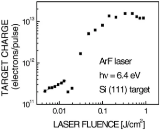
The expulsion of the nonthermal Si+ population is
in-duced by the formation of a positive charge on the silicon surface resulting from the emission of photoelectrons during UV laser irradiation. Figure3shows a time-integrated laser-induced charge on the target as a function of fluence. This charge has been evaluated by measuring a compensating cur-rent variation between the Si target and the ground38during laser pulse. From this figure, it can be seen that the target already accumulates a positive charge at low laser fluence, ⬃0.001 J/cm2. The charge increases almost linearly up to
saturation at a fluence of about 0.15– 0.2 J/cm2. Exactly at
FIG. 1. Time-of-flight spectra of Si+ions measured at different laser flu-ences. For 0.26 J/cm2, the vertical scale is expanded by a factor of 100.
FIG. 2. Experimental data on Si+yield vs laser fluence F
0. F0= 0.2 J/cm2 corresponds to the ion desorption threshold. Up to the melting threshold 共⬃0.4 J/cm2兲, the ion yield behaves as F
0
10.4, whereas at higher fluences, the dependence changes to F00.97. The solid curve corresponds to Eq.共27兲with
F0cr= 0.2 J/cm2.
FIG. 3. The measured laser-induced charge of the silicon target vs laser fluence.
these fluences, we detect the first nonthermal ions. Both the target charge saturation and ion ejection clearly indicate that the Si surface reaches critical conditions corresponding to the dynamical equilibrium between primary particle ejection 共photoelectrons兲 and desorption of the secondary species 共positively charged ions兲.
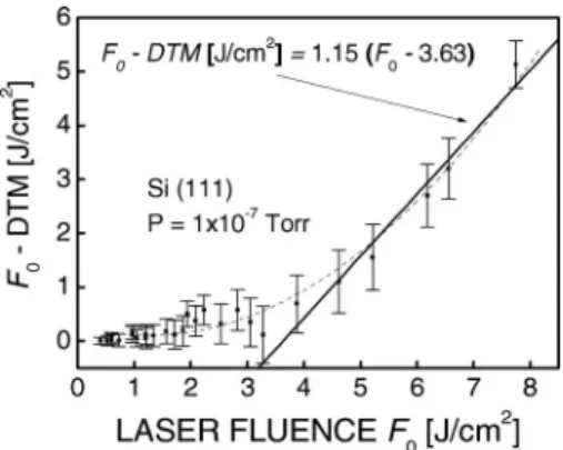
As a consequence, a part of the absorbed laser energy is used to produce the nonthermal Si+ population. This is re-vealed by evaluating a dynamical threshold of melting 共DTM兲 for various laser fluences using time resolved reflec-tivity measurements39on a hydrogen passivated Si共111兲 sur-face, under vacuum conditions. In these measurements, a He-Ne laser beam is focused on the irradiated Si target area and the temporal evolution of the reflected light is followed. At the instant of surface melting induced by ArF laser irra-diation, the reflected He-Ne laser beam intensity jumps to a higher value. Measuring this time from the start of the ArF laser pulse enables us to calculate the necessary fluence to melt a fixed number of Si layers. The obtained results on the DTM are shown in Fig.4as a function of ArF laser fluence. The increase in the DTM in the fluence range extending from the minimum static melting threshold of ⬃0.4 J/cm2 up to
⬃5 J/cm2 is in agreement with the absorption of laser
en-ergy by Si surface sites, leading to nonthermal ion ejection.40 Although for fluences higher than⬃0.4 J/cm2 the
nonther-mal population is less pronounced, its yield is still increasing approximately linearly with fluence 共see Fig.2兲. The DTM
decrease for high laser fluences共beyond ⬃5 J/cm2兲 was also
reported in Ref.39. It may be explained by the appearance of photoinduced plasma of free carriers, leading to a softening of the crystalline lattice. Then, the material can be in a qua-siliquid state even below its melting temperature,41,42 which consequently reduces the measured DTM. The difference be-tween the irradiation laser fluence F0 and the DTM
corre-sponds to the fluence part directly involved in the target heat-ing beyond meltheat-ing. This value is plotted versus laser fluence in Fig. 5. It is interesting to note that from the melting threshold 共⬃0.4 J/cm2兲 to the thermal ablation threshold 共⬃0.7–0.8 J/cm2兲, the 共F
0− DTM兲 value is close to zero,
indicating that the main part of the laser fluence is used in the melting process. Then, beyond the thermal ablation threshold, it starts to grow slowly, transforming to a strong nearly linear increase from a laser fluence of ⬃3.5 J/cm2.
Such a behavior with three regimes is consistent with the observations of Sanchez et al.43 on the ablation rate of Si under nanosecond ArF laser irradiation.
III. MODELING APPROACHES
The widely used modeling approach for the description of the nanosecond-laser pulse heating and the ablation of materials regardless of their kind is based on the thermal model in its different modifications, including those which take into account irradiation shielding by the generated plasma plume.24,25,44–46This relatively simple model gives a good description of experimental data on the material melt-ing and ablation thresholds and on mass removal without using any adjusting parameters or with a minimum adjust-ment which, however, can be physically founded. By being incorporated into a number of combined approaches,47–52 it has allowed a proper description of the interrelation between the target state and the laser-induced plume behavior includ-ing backward deposition of the ablated products.50,52 In the model, the absorption of the laser light by the target material is described by the following general Beer–Lambert law, which implies a linear relationship between the absorptance and the concentration of absorbing centers:
I共z兲 = I0exp共−␣abz兲, 共1兲
where I and I0are the local and incident laser intensities,␣ab is the absorption coefficient, and z is the laser beam propa-gation distance. This implies that the multiphoton processes as well as the free electrons generated in semiconductor and dielectric materials do not play a perceptible role in laser light absorption at the nanosecond regimes of laser irradia-tion. With the use of a thermal model, the spatial and tem-poral dynamics of laser heating, melting, and recrystalliza-tion can be revealed including the ablarecrystalliza-tion rates via the thermal mechanism and details concerning target superheat-ing. As soon as one is interested in the electronic mecha-nisms of ablation or in the influence of the free-electron population on the processes taking place in semiconductors or dielectrics under pulsed laser irradiation, a more sophisti-cated model is required for adequate analysis.
Let us first consider the processes triggered by a nanosecond-laser pulse in a semiconductor target. We will
FIG. 4. The DTM measured on a Si共111兲 surface under vacuum conditions as a function of incident laser fluence. The error bars correspond to the experimental uncertainty on the measurement of the melting moment.
FIG. 5. The difference between incident laser fluence F0and the DTM共the fluence fraction spent for heating the melted Si surface兲 as a function of incident laser fluence. The error bars correspond to the experimental uncer-tainty on the measurement of the melting moment.
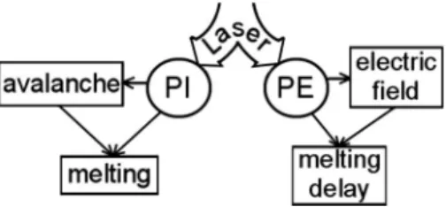
diverge from the assumption of local thermal equilibrium between the electron and lattice subsystems, which is usually implied for nanosecond-laser pulses, and consider the possi-bility of the violation of target quasineutrality due to electron photoemission. A simplified scheme of the processes is pre-sented in Fig. 6. A laser pulse acting on the target causes photoionization 共PI兲 and photoemission 共PE兲. These pro-cesses appear to be competitive with respect to target heating and melting. The electrons excited to the conduction band absorb laser radiation and can produce secondary electrons via collisional multiplication共avalanche兲. The free electrons, irrespective of their origin, interact with phonons and target heating takes place, which, at a definite level of the absorbed laser energy, gives rise to the melting process. This left branch of the processes is reasonably described by the sim-plified thermal model under the assumption of the linearity of laser light absorption. The right branch of the scheme shows the processes that are triggered by electron photoemis-sion and cannot be taken into account by thermal modeling. Photoemission depletes a superficial target layer, causing the violation of the target quasineutrality. This results in a posi-tive charging of the target as a whole and, thus, in the gen-eration of an ambipolar electric field. The electric field forces the charge carriers to relocate in order to neutralize the ex-cess positive charge. The rate of the neutralization proex-cess depends on a number of factors, which will be discussed below. All described processes were considered in the frames of the drift-diffusion approach 共the LISC model兲, approving the possibility of Coulomb explosion in dielectrics under femtosecond-laser irradiation14,30,31and showing such possi-bility for semiconductors under the action of nanosecond, UV laser pulses.31,32By depleting the target layer of the hot electron population and causing electronic desorption/ ablation, photoemission can retard the heating and melting processes. Below we compare the results of simulations based on the thermal and LISC models in order to test the relevance of the latter and show its advantages.
A. Thermal model
The details of the thermal model used in this paper have been described in Refs. 25and46. Here we repeat only its main features, dwelling on the thorough calculation of the solid-liquid interface.25,53 The time-dependent temperature distribution T共t,x兲 in the irradiated sample is governed by the heat-flow equation in a one-dimensional form as follows:
关cp+ Lm␦共T − Tm兲兴
冉
T t − u共t兲 T x冊
= x T x+␣abI共x,t兲. 共2兲 Here is the mass density of the target material, and cpand are the thermal capacity and the thermal conductivity of the target material, respectively. The laser pulse of a Gauss-ian temporal profile I共x,t兲 is attenuated exponentially along the target depth according to the Lambert–Beer law as fol-lows: I共x,t兲 = 共1 − R兲2F0
冑
ln 2 exp冋
− 4 ln 2冉
t 冊
2册
exp共−␣abx兲, 共3兲 where F0 is the laser fluence, is the laser pulse duration共FWHM兲, ␣ab and R are the absorption and reflection
coef-ficients, respectively, whose temperature-dependent values are taken from Ref.24, and x is the distance from the target surface toward the bulk depth. The term Lm␦共T−Tm兲 共Lmis
the latent heat of fusion兲 allows performing through calcula-tions of the liquid-solid interface,25,53 whose temperature is assumed to be continuous and equal to Tm. The ␦-function
was approximated as53 ␦共T − Tm,⌬兲 = 1
冑
2⌬exp冋
− 共T − Tm兲2 2⌬2册
, 共4兲with ⌬ depending on the temperature gradient 共the defini-tional domain of the ␦-function should be larger than three computational cells兲. u共t兲 is the velocity of surface recession, which is defined under the assumption that the flow of va-porized material from the surface follows the Hertz–Knudsen equation and the vapor pressure above the vaporized surface can be estimated with the Clausius–Clapeyron equation as follows: u共t兲 =pb
冉
m 2kTs冊
1/2 exp冋
Lv k冉
1 Tb − 1 Ts冊
册
. 共5兲Here the coefficient  accounts for the back flux of the va-porized particles to the target surface. Since low laser flu-ences near melting and vaporization thresholds are consid-ered here, we take= 1, assuming collisionless expansion of the ablation products. Also absorption of the laser irradiation by the laser-induced plasma plume is neglected. Lv is the latent heat of vaporization, k is the Boltzmann constant, and Tb is the boiling temperature under a reference pressure pb.
The parameters pband Tbare taken only as normalizing
val-ues and do not assume boiling as the vaporization mecha-nism.
The temperature behavior at the target boundary is gov-erned by the boundary condition assuming the possibility of thermal ablation:
冏
Tx
冏
x=0=u共t兲L. 共6兲When ablation is absent, this boundary condition is self-regulating to that accounting for the absence of heat flow through the target surface. Other conditions were as follows:
FIG. 6. A simplified scheme of the processes taking place in a silicon target under pulsed laser irradiation demonstrating their impact on the melting onset.
T共x,0兲=T0 and T共⬁,t兲=T0, where T0 is the initial 共room兲
temperature. Here we assume that the thermal wave does not reach the remote boundary during the calculation time. The used one-dimensional modeling is justified by the large irra-diation spot size as compared to the thermally affected target layer over the computational time.
B. Formulation of the LISC model for silicon irradiated by nanosecond, UV laser pulses
Our aim here is to describe the electron dynamics in the laser-irradiated silicon targets under conditions of the viola-tion of the quasineutrality caused by electron photoemission. This requires considering two interacting subsystems, elec-trons and lattice, while allowing charge separation in the irradiated sample. Hence, the model should include the con-tinuity equations for holes and free electrons, the equations describing charge-carrier transport, and the Poisson equation to calculate the electric field resulting from the violation of the quasineutrality. As was mentioned above, such an ap-proach was used to advantage in the analysis of conditions favorable to Coulomb explosion in dielectrics and semicon-ductors in different irradiation regimes, including femtosecond14,30,31 and nanosecond31,32 laser pulses. As shown in Ref.27, on a suprapicosecond time scale, the elec-tron and lattice subsystems can be described in terms of their temperatures, Teand Tl, respectively. In Ref.32, target
heat-ing was described usheat-ing Eq. 共2兲, implying Te= Tlas widely
accepted for fairly long laser pulses of nanosecond time scale. Here we focus on the heating, melting, and ablation aspects, particularly on electronic ablation. Supposing a strong charge separation and the possibility of incomplete thermal equilibrium, we use two energy equations for the electron and lattice subsystems and follow the electron-lattice relaxation process.
For a 193 nm laser wavelength 共photon energy ប = 6.4 eV兲, the continuity equations describing charge-carrier generation in silicon共band gap energy Eg= 1.17 eV兲 include
one-photon ionization and Auger recombination and is supplemented by a term describing the photoemission pro-cess as follows: ne t + 1 e Je x =␣ab I共x,t兲 ប na n0 + Qavna−␥ne2nh− PE na n0 , 共7兲 nh t + 1 兩e兩 Jh x =␣ab I共x,t兲 ប na n0 + Qavna−␥ne 2 nh. 共8兲
Here n and J are the density and the electric current, respec-tively; indices e, h, and a refer to electrons, holes, and neu-tral atoms; n0= na+ nh;␥ is the coefficient of Auger
recom-bination, and Qav is the temperature-dependent avalanche
rate.27Note that the one-photon ionization term is scaled for the available ionization centers in order to account for a pos-sible saturation of ionization. To calculate the charge-carrier transport in the target, the electric currents Je and Jh are
written in the drift-diffusion form as54
Je=兩e兩neeE − eDeⵜ ne, Jh=兩e兩nhhE − eDhⵜ nh.
共9兲 The diffusion coefficients are calculated as De= kTee/e and
Dh= kTeh/e, with Te representing the carrier temperature
andeandhbeing the electron and hole mobilities,
respec-tively. Here, for simplicity, we assume the mobilities of the electrons and holes in pure silicon to be constant and equal to the basic values 关e= 0.15 m2/共V s兲 and h
= 0.045 m2/共V s兲 共Ref. 55兲兴. In fact, the electron and hole
mobilities in silicon are decreasing functions of both the tem-perature and the electric field, at least in the measured ranges 共up to 600 K and 106V/m, respectively兲.54
However, under the conditions studied in this paper, when Teand E values are
typically much higher, the charge-transport parameters of silicon are poorly known. Test modeling with ten times re-duced mobilities for the electrons and holes has not demon-strated a significant impact on the resulting charging and melting behaviors. Consequently, by emphasizing a qualita-tive picture of our modeling, we abandon speculating ap-proximations of the mobilities and stay here at their basic values.
The electron photoemission term for UV laser irradia-tion, when photon energy well exceeds the sum of the band gap and the work function, can be written as
PE =1 2␣ab I共x,t兲 ប exp
冉
− x lPE冊
, 共10兲where lPE= 12 Å is the electron escape depth.56 Expression
共10兲 implies that the generated electrons with the normal momentum component directed to the surface can escape into vacuum. Thus, by taking into account the equilibrium angular distribution for the carrier momenta established at nanosecond-laser irradiation conditions,31,32we assume that, on average, half of the electrons produced through the one-photon ionization are immediately photoemitted from the surface region.
The photoemission and diffusion terms lead to charge separation in the target, resulting in electric field共E兲 genera-tion described by the following Poisson equagenera-tion:
E
x = e 0
共nh− ne兲, 共11兲
with a boundary condition defined by Gauss law. In Eq.共11兲, is the dielectric permittivity of bulk silicon. In order to better satisfy the stability of the numerical procedure, Eqs.
共9兲and共11兲are introduced into Eqs.共7兲 and共8兲, composing the final form of the continuity equations:
ne t −ene e 0 共nh− ne兲 −eE ne x − xDe ne x =␣ab I共x,t兲 ប na n0 + Qavna−␥ne 2 nh− PE na n0 , 共12兲
nh t +hnh e 0 共nh− ne兲 +hE nh x − xDh nh x =␣ab I共x,t兲 ប na n0+ Qavna−␥ne 2 nh. 共13兲
Instead of the simplified expression共3兲 for light attenuation within the bulk, the Beer–Lambert equation was solved tak-ing into account the depletion of the ground state durtak-ing irradiation as follows: xI共x,t兲 = −␣abI共x,t兲 na n0 . 共14兲
The energy equation for free electrons is written taking into account that the electrons generated through a one-photon ionization have an initial energy equal to the differ-ence of the photon and band gap energies. The Auger recom-bination process results in heating the free-electron subsystem. Also it is assumed that the photoemitted electrons escape from the target, bringing away the average free-electron energy. Hence, the final form of the free-electron energy equations is as follows: Ef t =共ប− Eg兲 ␣abI共x,t兲 ប na n0 − EePE na n0 + Eg␥ne 2 nh. 共15兲
Here Ef= neEeis the energy density of the free-electron
sub-system, with Ee the average electron energy. The electron
energy transport within the target is expressed in terms of the heat-flow equation as follows:
Ae
冉
Te t + Je ene Te x冊
= xKe Te x − g共Te− Tl兲 + ⌺共x,t兲, 共16兲 where Ae= 3k/2 is the free-electron heat capacity, Ke= 2k2eTe/e is the thermal conductivity of the electrons,27 g
is the electron-phonon coupling constant, and ⌺共x,t兲 is the source term, which has the following form:31
⌺共x,t兲 =Ee t = 1 ne
冉
Ef t − 3 2kTe ne t冊
. 共17兲The heat-flow equation for the lattice is written as 关cp+ Lm␦共T − Tm兲兴 Tl t = x Tl x + g共Te− Tl兲. 共18兲 The value l= g/Ae is the hot carrier relaxation time and is
taken to be 0.5 ps.57 The surface recession velocity via the electronic ablation mechanism ue共t兲 will be introduced below
in Sec. III D.
For solving the system of equations共10兲–共18兲, we use an explicit numerical scheme on an irregular grid, dense in the near-surface absorption region 共the numerical cells ⌬x are 5 Å wide兲 and rarefying toward the remote boundary with a factor of 1.01. At the remote boundary, the absence of the electron flow is allowed assuming a floating sample. The time step⌬t is selected empirically to better satisfy the nu-merical scheme stability and the approximation of the origi-nal equations.
C. Analysis of surface charging
A rough estimation of the electron photoemission yield through a unit surface area共NPE兲 from the target of thickness
L can be obtained by the integration of the photoemission term 共10兲over time and space共the time moment t=0 corre-sponds to the center of the Gaussian profile of the laser beam兲 as follows: NPE=
冕
−⬁ ⬁冕
0 L PEdtdx. 共19兲By substituting Eqs.共3兲and共10兲into Eq.共19兲and neglecting the change in the reflection and absorption coefficients upon melting of the target surface, we have
NPE= 1 2q␣ab共1 − R兲F0 兵1 − exp关− 共␣ab+ lPE−1兲L兴其 共␣ab+ lPE −1兲 , 共20兲 or at LⰇ␣ab −1
, which is our case, NPE= ␣ab共1 − R兲F0
2q共␣ab+ lPE
−1兲. 共21兲
Under the assumption that there is no supply of electrons from the radiation-free sides of the target, the electric field generated on the target surface can be estimated by using Gauss law. The residual positive charge of the target is equal to the charge of electrons having left the target. For a plane target with the charge density q共x兲=−e关nh共x兲−ne共x兲兴
gener-ated to the end of the laser pulse, this gives 兩E兩x=0= 1 20
冕
0 L q共x兲dx = eNI 20 =eNPE 20 , 共22兲where NIis the number of excess positive ions共holes兲
accu-mulated in the target per unit surface area. Note that the value of the electric field in vacuum above the surface is times higher than that in the target. Finally, we obtain an estimate of the maximum electric field generated on the sur-face of the unearthed silicon sample under the considered conditions:
兩E兩x=0= e␣ab共1 − R兲F0 40q共␣ab+ lPE
−1兲. 共23兲
The electric field that must be exceeded in order to break the atomic bonds 共the critical field兲 can be found as31,32
兩Ecr兩x=0=
冑
2⌳atn0 0, 共24兲
where n is the number density of the lattice and ⌳atis the
energy necessary to impart on an atom in order to remove it from the target. By using the latent heat of vaporization for silicon 关16 115 J/g 共Ref.58兲兴 to estimate the ⌳atvalue, we
obtain from Eq. 共24兲 Ecr⬇2.65⫻1010V/m. By comparing
Eqs. 共21兲, 共22兲, and 共24兲, we find the value of the critical laser fluence, starting from which nonthermal ion emission can be expected as a result of high surface charging:
F0cr=
40qEcr共␣ab+ lPE −1兲
e␣ab共1 − R兲
. 共25兲
With lPE= 12 Å, we obtain F0cr⬃0.15 J/cm2. This value is
only somewhat lower than that obtained in the experiments 共0.2 J/cm2兲. Expression共25兲has been obtained for an ideal
one-dimensional case, disregarding the electron and hole drift during the laser action. Electrons arriving at the surface layer in order to neutralize the excess positive charge should tend to increase the critical laser fluence. A more sophisti-cated picture of the processes can be obtained within the LISC model as described in Sec. III B.
The number of ions emitted from the target by the elec-trostatic force can be estimated by calculating the accumu-lated positive charge in excess of the value necessary for the generation of the critical electric field:
Nexp= NI− NIth=
␣ab共1 − R兲共F0− F0cr兲SR
2q共␣ab+ lPE
−1兲 , 共26兲
with SR being the irradiated spot area. Under our irradiation
conditions共SR= 0.5 mm2兲, this gives
Nexp⬃ 1.38 ⫻ 1014共F0− F0cr兲, 共27兲
where laser fluence is in J/cm2. In Fig.2, the nonthermal ion
yield estimated from Eq. 共27兲 with F0cr= 0.2 J/cm2 is
pre-sented by a solid line as a function of laser fluence, showing the same general tendency as obtained in the experiments.
D. The rate of electronic ablation
As soon as the critical electric field is reached in the surface target layer, positive ion ejection is initiated as an inevitable process for relieving the target of the electrostatic stress. At nanosecond-laser pulse regimes, a continuous elec-tron photoemission can lead to a continuous ion emission in contrast to femtosecond irradiation regimes, where the elec-trostatic disintegration 共called Coulomb explosion兲 can be considered as a synchronous effect for several superficial monolayers.14,30 Under nanosecond-laser irradiation, non-thermal ion emission is an extended process that lasts from the generation of the critical electric field until the partial neutralization of the excess positive charge by the electron supply from deeper target layers, or until laser pulse termi-nation, or, for fluences above the melting threshold, until the melting moment since band gap collapse due to melting should lead to a rapid electron relocation and the screening of the electric field. Besides, melting gives an alternative mechanism of stress relieving by means of thermal vaporiza-tion, as described by Eq. 共5兲. In the time interval from the generation of the critical electric field until target surface melting, the electric field at the surface does not exceed the critical value due to immediate ion emission or due to charge relocation. In terms of the LISC model formulated in Sec. III B and III C, the electronic emission rate ue共t兲 has to be
introduced, which would prevent the electric field growth above the critical value.
The electronic rate of ablation can be written as ue
=s/t, where s is the momentary position of the target sur-face coinciding with the position E = Ecr 共in the case of Es
⬍Ecr, ue= 0兲. For metal and semiconductor targets, the
elec-tric field generated in the sample decays quasiexponentially with the distance toward the target depth.31 Hence, we can assume that E共x,t兲=Es共0,t兲exp共−x/xc兲, where Es共0,t兲 and xc
are the surface electric field and the characteristic length of its decay, respectively. For a rough numerical grid 共here ⌬x = 5 Å兲, the value xc can be evaluated from the calculated
value of the electric field at the point x =⌬x as xc=
−⌬x/ln关E共⌬x,t兲/Es共0,t兲兴. We assume that, during the time
step⌬t, the surface electric field has increased from Ecrto Es.
Consequently, the position of the critical field共and, hence, a new position of the target surface兲 can be determined as
xs=⌬x
ln关Ecr/Es共0,t兲兴
ln关E共⌬x,t兲/Es共0,t兲兴
. 共28兲
Then, the final finite-difference form of the electronic abla-tion rate can be written as
ue共t兲 = ⌬x ⌬t ln关Ecr/Es共0,t兲兴 ln关E共⌬x,t兲/Es共0,t兲兴 . 共29兲
Substituting the terms f/t 关for f =共ne, nh, Te, Tl, Ef兲兴 by
关f/t − ue共t兲f/x兴 in Eqs.共12兲,共13兲, and共15兲–共18兲, we
ob-tain the LISC model with the target—vacuum interface mov-ing due to the electronic mechanism of surface recession. Simulations have shown that, indeed, Eq. 共29兲 provides for the fulfillment of the condition Es共0,t兲=Ecr as soon as the
electronic ablation mechanism is realized.
IV. MODELING RESULTS AND DISCUSSION
The simulations on the basis of the LISC model were performed for the laser fluence range of 0.2– 2 J/cm2. As-suming that the heated surface atoms having a certain vibra-tional energy can escape from the sample with a greater probability than the cold ones, a more correct expression for the critical field is used31
兩Ecr兩x=0=
冑
2共⌳at− cpTl兲n0
0
. 共30兲
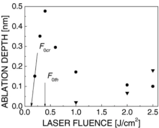
The results of modeling are presented in Figs.7–11. Accord-ing to both models, the meltAccord-ing threshold fluence for silicon irradiated by the nanosecond-laser pulses 共193 nm wave-length兲 is ⬃0.4 J/cm2 共Fig.7兲, which is in good agreement
with Ref. 24. The electronic model was applied only for a
FIG. 7. Ablation depths obtained in the frames of the LISC model共circles兲 and the thermal model共triangles兲.
time interval of the laser pulse action before reaching the melting temperature at the target surface. Already at 0.2 J/cm2, which is well below the melting threshold, the electronic surface recession takes place, removing less than one monolayer of substance共Fig.7兲 in accordance with the
estimations presented in Sec. III C. The calculated threshold for electronic ablation F0cr共shown in Fig.7by an arrow兲 is also in good agreement with the analytical estimate obtained in Sec. III C. At the melting threshold fluence 共0.4 J/cm2兲,
the maximum of electronic ablation is reached when almost 2.5 monolayers of silicon共4.8 Å兲 are removed. At fluences above the melting threshold, the electronic ablation depth
decreases, giving way to the thermal ablation mechanism. Consequently, at low fluences, only the nonthermal compo-nent of the ablation products is present while, with melting, the thermal component is superimposed on the nonthermal one共Fig.7兲. Note that thermal ablation is weak at the studied
fluence range. The thermal model shows that thermal vapor-ization with the removal of dozens to hundreds of monolay-ers develops only at fluences 艌3 J/cm2, in agreement with our experimental observations, as reported in Fig.5共see Sec.
II兲.
Thus, as a whole, the LISC model describes adequately the main features of electronic ablation observed in the ex-periments with the exception of the total ablation yield 共cf. Figs.2and7兲. Indeed, according to the simulations, the total
ablation depth 共thermal and electronic兲 decreases with flu-ence in the range of 0.4– 1 J/cm2, stabilizing at a low value
FIG. 8. 共a兲 Calculated temporal evolution of the electric field generated on the surface of the silicon target irradiated by nanosecond, UV laser pulse at 1 J/cm2共solid line兲. The laser pulse is centered at t=0, while melting occurs at t = −3.7 ns. The critical electric field according to the temperature-dependent criterion given by Eq.共30兲is reached at −5.8 ns共shown by arrow A兲, whereupon the electronic ablation keeps it nearly constant. Neglecting the temperature dependence of the critical electric field关Eq.共24兲兴 leads to a delay of the electronic ablation process共dotted line, arrow B兲. 共b兲 Distribu-tion of the electric field in the bulk at t = −5.7 ns showing that the field is generated in a few superficial monolayers of the material.
FIG. 9. Calculated spatial profiles of the electron 共solid line兲 and hole 共dashed line兲 densities in the Si target for the same conditions as in Fig.8
共t=−5.7 ns兲. The strong electron depletion of the surface layer results in suppressed Auger recombination and, correspondingly, to extremely high surface charging.
FIG. 10. Temporal evolution of the lattice temperature obtained within the frames of the LISC共solid line兲 and thermal 共dashed line兲 models. The re-sults on the LISC model are presented until the melting onset. The shape of the laser pulse is shown by the dotted line. The inset demonstrates details of the difference in the heating dynamics obtained with the two models in the vicinity of the melting point. The regime corresponds to Figs.8and9.
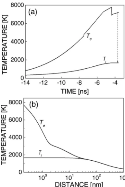
FIG. 11.共a兲 Temporal behavior and 共b兲 spatial distribution at t=−5 ns of the electron and lattice temperatures for the laser-irradiation regime as in Figs.
8–10showing the considerable nonequilibrium between the electron and lattice subsystems in the superficial target layer.
for higher fluences until the thermal ablation mechanism be-comes dominant at F0⬎2 J/cm2, whereas the measured ion
yield is a growing function of fluence. This can be attributed to the separate consideration of electronic and thermal abla-tions. We assume that electronic ablation terminates with the melting onset, and the generated electric field does not influ-ence the thermal ablation process. However, it can be specu-lated that the positive charge accumuspecu-lated on the sample sur-face before the melting onset further promotes the ablation process, leading to a combined ablation mechanism, charge-assisted thermal ablation. Note that the residual charge pro-vides a strong, near-critical electric field关Eq.共30兲兴. The fact that the thermal model well describing the developed nano-second regime of ablation overestimates the ablation thresh-old fluence is indicative of this charge-assisted mechanism of thermal ablation.59–61A joint consideration of the two abla-tion mechanisms, electronic and thermal, which is extremely arduous, is beyond the limits of the proposed modeling ap-proach. Below we will discuss what can be learned about the electron dynamics and the electric field generation in a laser-irradiated silicon sample with the use of the LISC model and its comparison with the purely thermal model.
Figure8共a兲shows the temporal evolution of the electric field generated during the laser pulse with F0= 1 J/cm2until
the melting onset, which takes place at the time t = −3.75 ns relative to the laser pulse maximum. Already before surface melting, the critical electric field has been reached in the surface layer 共at t=−5.8 ns兲, giving way to the electronic mechanism of ablation 关solid line in Fig. 8共a兲兴. Note that modeling with the electronic ablation criterion in the form
共24兲delays the ablation process by 0.5 ns as compared to the temperature-dependent Ecr 关Eq. 共30兲兴. During the next
1.55 ns until the melting onset, almost one monolayer of silicon atoms共mainly in the form of positive ions as shown below兲 is emitted from the surface. The electric field is con-centrated in a very narrow near-surface layer 关Fig.8共b兲, for t = −3.8 ns兴 with exponential decay toward the bulk, in accor-dance with a metallic behavior tending to accumulate the access charge on the surface.31 Indeed, Fig.9 demonstrates that the excess positive charge is accumulated in a surface layer ⬃2 nm wide. In this zone, a very high ionization de-gree is reached. The hole density on the surface is nh⬇2.2
⫻1022cm−3, which corresponds to the ratio n
h/n0= 45%,
which is unusual for silicon at nanosecond irradiation re-gimes. It is widely believed that, under such regimes, the Auger recombination process regulates the free-electron den-sity to a subcritical value. However, as discussed above, the superficial target layer is depleted of electrons due to photo-emission, which results in the suppression of Auger recom-bination. Continuing the irradiation of the nanosecond-laser pulse leads to further ionization, which is not balanced by recombination. In turn, this leads to material softening and electronic surface recession.
It should be underlined that the described electronic mechanism of ablation/desorption at nanosecond irradiation regimes can be completely attributed to a short wavelength of laser irradiation that provides one-photon electron photo-emission. For longer laser wavelengths leading to a multi-photon photoemission process, laser fluences near the
melt-ing threshold cannot produce photoemission yields large enough for substantial target charging. Another feature of UV laser irradiation favoring the electronic mechanism of ablation is a small absorption length 共⬃60 Å for = 193 nm兲. The simulations show that, already at a depth of ⬃0.2m below the surface, the charge-carrier density cor-responds to the intrinsic one 共1.5⫻1010cm−3兲. For UV nanosecond-laser pulses, this provides favorable conditions for strong surface charging because of a negligible electronic supply from the bulk depth. It should be mentioned that, for UV femtosecond-laser pulses, the short absorption length leads to a strong localization of the laser energy in a thin target layer, resulting in extremely low melting thresholds, well below significant surface charging, and in phase explo-sion as the most probable ablation mechanism.31
It is interesting that the photoemission term scaled to the neutral atom density in Eqs. 共12兲 and 共15兲 assumes a self-regulation mechanism of photoemission at high values of the electric field. As soon as the electric field energy density reaches a value of the order of 1 eV/atom and can noticeably influence the electron work function, the density of neutrals decreases, causing a decrease in the photoemission rate. As a result, the number of electrons that escape from the irradia-tion spot is saturated at overcritical laser fluences 共⬎0.2 J/cm2兲 and, for the irradiation spot size of 0.5 mm2at
F0= 1 J/cm2, the calculated photoelectron yield is ⬃2.2
⫻1013, in excellent agreement with the measured electric
residue共Fig.3兲.
Figure10presents the lattice temperature behavior in the case of laser irradiation obtained by using the two models, thermal共dashed line兲 and LISC 共solid line兲. The shape of the laser pulse is given by the dotted line. It is seen that the LISC model gives a very good approximation of the thermal model, showing only a slight lag in heating. This lag is at-tributed to a partial loss of the laser energy due to the pho-toemission and surface recession processes. Indeed, the cal-culations have shown that by setting PE= 0 in Eqs.共12兲and
共15兲, we obtain exact concordance between the two models. Increased deviation between the temperatures obtained in the frames of two models occurs when the melting point is being approached. A comparison with Fig.8共a兲shows that the elec-tric field reaches its critical value, giving rise to electronic ablation. The inset in Fig.10gives a more detailed difference between the results obtained, with the two models demon-strating a melting delay of⬃1 ns for the case when the pho-toemission process and electronic target recession are taken into account. An integration of the laser pulse shows that this seemingly weak delay actually corresponds to a substantial increase in laser energy coupled to the target until the melt-ing onset exceeds 20% as compared to thermal modelmelt-ing. This value is apparently smaller than that measured in the experiments 共see Figs.4and5兲; however, it shows that,
in-deed, the electronic mechanism of ablation of semiconductor targets can play a perceptible role in the overall balance of the laser energy.
It should be emphasized that the continuum approach used here can considerably underestimate the studied effects by disregarding the subtle surface processes such as the re-moval of adatoms and surface dimers, which have lower
binding to the surface and can be removed by an electric field well below the critical one. Another issue concerns the strong concentration of holes in the surface layer, which is observed in Fig. 9 and points to the accumulation of anti-bonding states on the surface, which favor bond rupture and ion emission.11,62These two factors can significantly contrib-ute in increasing the laser energy necessary to produce sur-face melting and, thus, to further delay the melting moment during the laser pulse.
An important result obtained in the frames of the LISC model is the absence of equilibrium between the electron and lattice subsystems in the absorption zone. The temporal be-havior of the electron and lattice temperatures at the surface and their spatial distributions are given in Fig. 11 for F0
= 1 J/cm2. It is seen that with heating time, the electron tem-perature deviates from that of the lattice, exceeding the latter by four to five times. One can notice sudden jumps in the electron temperature experienced during heating关Fig.11共a兲兴.
They can be attributed to the ultrafast dynamics of free elec-trons in the superstrong electric field. The electron diffusion, which is extremely weak in the depth of the order of several dozens of nanometers, can play, however, some role in the surface layer, where the electron temperature reaches values of 7000– 8000 K. When reaching a value competitive with the drift term in Eq.共9兲, the diffusion term causes a sudden relocation to the surface of colder electrons from deeper tar-get regions. After balancing between the drift and diffusion, the electron temperature increases until the melting moment. As soon as melting takes place, leading to the band gap collapse, the strong increase in the conduction band popula-tion should lead to a rapid equilibrapopula-tion between the electron and lattice subsystems, as shown by the arrow关Fig.11共a兲兴.
Figure 11共b兲 demonstrates that the nonequilibrium be-tween the electrons and the lattice takes place in a layer 30 nm thick, where the main absorption of the laser light occurs. In deeper layers where the energy is transported via thermal conduction, the electron and lattice temperatures are equal. The enhanced electron temperature in the electron es-cape zone can also contribute to the increased electric field via the thermal emission mechanism. This is an additional point in favor of a significant effect of charge-carrier trans-port on the dynamic melting threshold in silicon under nanosecond-laser ablation reported in this study.
V. CONCLUSIONS
We have studied experimentally and theoretically an electronic mechanism of desorption and ablation of silicon under irradiation by nanosecond-laser pulses. Different as-pects of the dynamics of laser-induced target heating, melt-ing, and ablation have been analyzed, both thermal and elec-tronic: laser light absorption, electron and lattice heat conduction, electron photoemission, generation of the ambi-polar electric field, and charge-carrier transport within the target. The electronic ablation rate has been introduced into the LISC model, which has enabled describing the surface recession below the melting point. It has been shown that the electron photoemission process can play a significant role in overall target behavior, leading to an enhanced laser energy
necessary to reach melting and to the violation of the thermal equilibrium between the electron and lattice subsystems. Fur-ther development of the model implies the introduction of a number of improvements such as thermal electron emission and a criterion for adatom emission. More features of the electron dynamics could be learned within a kinetic ap-proach, which could enable considering the ballistic elec-trons. However, the present model has revealed an important role of the charge-carrier effect in nanosecond laser-irradiated silicon and its conclusions can be extended to other semiconductor materials.
ACKNOWLEDGMENTS
The authors would like to thank A. V. Bulgakov and R. Kronquist for valuable discussion. Partial financial support from INTAS and SB RAS共INTAS Project No. 06-1000013-8949兲 and RFBR 共Project No. 06-08-01196兲 are gratefully acknowledged.
1C. V. Shank, R. Yen, and C. Hirlimann,Phys. Rev. Lett.51, 900共1983兲. 2P. Stampfli and K. H. Bennemann,Phys. Rev. B49, 7299共1994兲. 3K. Sokolowski-Tinten, J. Bialkowski, and D. von der Linde,Phys. Rev. B
51, 14186共1995兲.
4S. I. Kudryashov and V. I. Emel’yanov, JETP Lett. 73, 228共2001兲. 5A. Rousse, C. Rischel, S. Fourmaux, I. Uschmann, S. Sebban, G. Grillon,
Ph. Balcou, E. Förster, J. P. Geindre, P. Audebert, J. C. Gauthier, and D. Hulin,Nature共London兲410, 65共2001兲.
6J. Bonse, S. Baudach, J. Krüger, W. Kautek, and M. Lenzner,Appl. Phys.
A: Mater. Sci. Process.74, 19共2002兲.
7J. Bonse, K.-W. Brzezinka, and A. J. Meixner,Appl. Surf. Sci.221, 215 共2004兲.
8J. Eizenkop, I. Avrutsky, G. Auner, D. G. Georgiev, and V. Chaudhary,J.
Appl. Phys.101, 094301共2007兲.
9O. Varlamova, F. Costache, J. Reif, and M. Bestehorn,Appl. Surf. Sci.
252, 4702共2006兲.
10M. Guillermin, F. Garrelie, N. Sanner, E. Audouard, and H. Soder, Appl. Surf. Sci. 253, 8075共2007兲.
11J. Kanasaki, A. Okano, K. Ishikawa, Y. Nakai, and N. Itoh, Nucl. Instrum. Methods Phys. Res. B 101, 93共1995兲.
12R. Stoian, D. Ashkenasi, A. Rosenfeld, and E. E. B. Campbell,Phys. Rev.
B62, 13167共2000兲.
13D. J. Lim, H. Ki, and J. Mazumder,J. Phys. D39, 2624共2006兲. 14R. Stoian, A. Rosenfeld, D. Ashkenasi, I. V. Hertel, N. M. Bulgakova, and
E. E. B. Campbell,Phys. Rev. Lett.88, 097603共2002兲.
15M. Henyk, F. Costache, and J. Reif,Appl. Surf. Sci.186, 381共2002兲. 16S. Amoruso, G. Ausanio, R. Bruzzese, L. Gragnaniello, L. Lanotte, M.
Vitiello, and X. Wang, Appl. Surf. Sci. 252, 4863共2006兲.
17H. Dachraoui and W. Husinsky,Phys. Rev. Lett.97, 107601共2006兲. 18S. Paul, S. I. Kudryashov, K. Lyon, and S. D. Allen,J. Appl. Phys.101,
043106共2007兲.
19A. Kasuya and Y. Nishina, Phys. Rev. Lett. 57, 755共1986兲.
20A. V. Bulgakov, I. Ozerov, and W. Marine, Thin Solid Films 453–454, 557 共2004兲.
21A. V. Bulgakov, I. Ozerov, and W. Marine, Appl. Phys. A: Mater. Sci. Process. 79, 1591共2004兲.
22R. Stoian, A. Mermillod-Blondin, N. M. Bulgakova, A. Rosenfeld, I. V. Hertel, M. Spyridaki, E. Koudoumas, P. Tsanetakis, and C. Fotakis,Appl. Phys. Lett.87, 124105共2005兲.
23V. Hommes, M. Miclea, and R. Hergenröder, Appl. Surf. Sci. 252, 7449 共2006兲.
24S. De Unamuno and E. Fogarassy,Appl. Surf. Sci.36, 1共1989兲. 25N. M. Bulgakova, A. V. Bulgakov, and L. P. Babich, Appl. Phys. A: Mater.
Sci. Process. 79, 1323共2004兲.
26E. J. Yoffa,Phys. Rev. B21, 2415共1980兲. 27H. M. van Driel,Phys. Rev. B35, 8166共1987兲.
28T. Held, T. Kuhn, and G. Mahler,Phys. Rev. B44, 12873共1991兲. 29S. S. Mao, X.-L. Mao, R. Greif, and R. E. Russo, Appl. Surf. Sci. 127–
129, 206共1998兲.
Campbell,Phys. Rev. B69, 054102共2004兲.
31N. M. Bulgakova, R. Stoian, A. Rosenfeld, I. V. Hertel, W. Marine, and E. E. B. Campbell,Appl. Phys. A: Mater. Sci. Process.81, 345共2005兲.
32W. Marine, N. M. Bulgakova, L. Patrone, and I. Ozerov, Appl. Phys. A: Mater. Sci. Process. 79, 771共2004兲.
33G. S. Higashi, Y. J. Chabal, G. W. Trucks, and K. Raghavachari,Appl.
Phys. Lett.56, 656共1990兲.
34The melting threshold was determined from time resolved reflectivity measurements performed from the same targets under vacuum conditions. The measured value of 0.4 J/cm2is in good agreement with the one re-ported in Ref. 24. See also L. Patrone, Ph.D. thesis, University Aix-Marseille II, 2000.
35A. V. Bulgakov, W. Marine, O. F. Bobrenok, and I. Ozerov共unpublished兲. 36J. T. Dickinson, S. C. Langford, J.-J. Shin, and D. L. Doering,Phys. Rev.
Lett.73, 2630共1994兲.
37F. Stietz, M. Stuke, J. Viereck, T. Wenzel, and F. Trager,Appl. Surf. Sci.
129, 64共1998兲.
38W. Marine, M. Gerry, P. Thomsen-Schmidt, and J. M. Scotto d’Aniello,
Appl. Surf. Sci.69, 290共1993兲.
39W. Marine and P. Mathiez, IEEE J. Quantum Electron. 22, 1404共1986兲. 40A more complete analysis shows that further mechanisms such as spatial
photon energy redistribution towards hot carriers共see Ref.39兲 must be
considered to account for such a DTM increase with laser fluence. The diffusion of these hot carriers deeper into the substrate, which results in volume heating of the lattice, tends to decrease the efficiency of surface heating.
41J. A. van Vechten, R. Tsu, and R. W. Saris,Phys. Lett.74A, 422共1979兲. 42B. Dragnea and B. Bourguignon,Phys. Rev. Lett.82, 3085共1999兲. 43F. Sanchez, J. L. Morenza, R. Aguiar, J. C. Delgado, and M. Varela,Appl.
Phys. Lett.69, 620共1996兲.
44V. N. Tokarev, J. G. Lunney, W. Marine, and M. Sentis,J. Appl. Phys.78, 1241共1995兲.
45S. Fähler and H.-U. Krebs, Appl. Surf. Sci. 96–98, 61共1996兲.
46N. M. Bulgakova and A. V. Bulgakov, Appl. Phys. A: Mater. Sci. Process.
73, 199共2001兲.
47J. Neamtu, I. N. Mihailescu, C. Ristoscu, and J. Hermann, J. Appl. Phys.
86, 6098共1999兲.
48A. V. Gusarov, A. G. Gnedovets, and I. Smurov,J. Appl. Phys.88, 4352 共2000兲.
49T. E. Itina, J. Hermann, P. Delaporte, and M. Sentis, Phys. Rev. E66, 066406共2002兲.
50N. Y. Bykov, N. M. Bulgakova, A. V. Bulgakov, and G. A. Loukianov, Appl. Phys. A: Mater. Sci. Process. 79, 1097共2004兲.
51Z. Zhang and G. Gogos,Phys. Rev. B69, 235403共2004兲. 52A. A. Morozov,Appl. Phys. A: Mater. Sci. Process.79, 997共2004兲. 53S. P. Zvavyi and G. D. Ivlev, Inzh.-Fiz. Zh. 69, 790共1996兲 共in Russian兲. 54B. Van Zeghbroeck, Principles of Semiconductor Devices, 2004, http://
ece-www.colorado.edu/bart/book/
55R. E. Hummel, Electronic Properties of Materials共Springer-Verlag, Ber-lin, 1993兲.
56C. Sebenne, D. Bolmont, G. Guichar, and M. Balkanski,Phys. Rev. B12, 3280共1975兲.
57T. Sjodin, H. Petek, and H.-L. Dai,Phys. Rev. Lett.81, 5664共1998兲. 58Properties of Elements: Handbook, edited by M. E. Drits共Metallurgiya,
Moscow, 1985兲 共in Russian兲.
59E. F. Lazneva, Laser Desorption 共Izdatelstvo Leningradskogo Univer-siteta, Leningrad, 1990兲 共in Russian兲.
60E. F. Lazneva, Radiat. Eff. Defects Solids 115, 257共1991兲. 61A. V. Bulgakov, personal communication共June 21, 2007兲.