HAL Id: tel-01752618
https://hal.univ-lorraine.fr/tel-01752618
Submitted on 29 Mar 2018
HAL is a multi-disciplinary open access archive for the deposit and dissemination of sci-entific research documents, whether they are pub-lished or not. The documents may come from teaching and research institutions in France or abroad, or from public or private research centers.
L’archive ouverte pluridisciplinaire HAL, est destinée au dépôt et à la diffusion de documents scientifiques de niveau recherche, publiés ou non, émanant des établissements d’enseignement et de recherche français ou étrangers, des laboratoires publics ou privés.
Characterization and improvement of silicon solar cells :
enhanced light acceptance and better separation and
extraction of charge-carriers
David Klein
To cite this version:
David Klein. Characterization and improvement of silicon solar cells : enhanced light acceptance and better separation and extraction of charge-carriers. Other [cond-mat.other]. Université Paul Verlaine - Metz, 2009. English. �NNT : 2009METZ003S�. �tel-01752618�
AVERTISSEMENT
Ce document est le fruit d'un long travail approuvé par le jury de
soutenance et mis à disposition de l'ensemble de la
communauté universitaire élargie.
Il est soumis à la propriété intellectuelle de l'auteur. Ceci
implique une obligation de citation et de référencement lors de
l’utilisation de ce document.
D'autre part, toute contrefaçon, plagiat, reproduction illicite
encourt une poursuite pénale.
Contact : [email protected]
LIENS
Code de la Propriété Intellectuelle. articles L 122. 4
Code de la Propriété Intellectuelle. articles L 335.2- L 335.10
http://www.cfcopies.com/V2/leg/leg_droi.php
THESE DE DOCTORAT
Présenté par
David KLEIN
En vu de l’obtention du diplôme de
Docteur
de l’université Paul Verlaine de Metz et de la Freie Universität de Berlin
dans le cadre d’une cotutelle
_____________________________________
Characterization and improvement of silicon solar cells:
Enhanced light acceptance and better separation and extraction
of charge-carriers.
_____________________________________
Soutenue le vendredi 27 février 2009 devant la commission d’examen:
Marinus KUNST Directeur de
recherche, HZB
Président du jury
Jocelyn HANSSEN Professeur à l’Université de Metz
Co-directeur de thèse
William BREWER Professeur à la FreieUniversität de
Berlin Co-directeur de thèse
Aotmane EN NACIRI Maitre de conférences
Frank WÜNSCH Dr. HDR,
Helmholtz-Zentrum Berlin Examinateur
Paul FUMAGALLI Professeur à la FreieUniversität de
Berlin Rapporteur
Omar Ariel FOJÓN Professeur à l’Universidad de Rosario
Rapporteur
Abstract
This work studies Silicon nitride and its electrical passivation and anti-reflection properties on n-type and p-type mono crystalline silicon for its use as light entrance window of an inverted a-Si:H/c-Si heterocontact solar cell in the frame of the development of low cost, high efficiency solar cells. Comparative investigation on silicon dioxide and amorphous silicon coatings were performed.
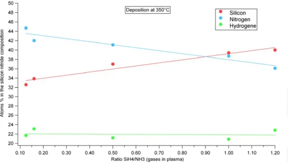
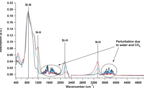
Silicon nitride is deposited by plasma enhanced chemical vapour deposition and was investigated by various measurement methods. The modifications induced by variation of the precursor gas mixture (Silane, Ammoniac and Nitrogen) on the composition were measured by Elastic Recoil Detection Analysis (ERDA). Correlation between the composition and the optical and electrical properties were studied (Fourier Transform InfraRed (FTIR) spectroscopy, XPS, …) and simulated. Evolution of the thickness and refractive indices were measured by ellipsometry. Measurements of the reflection, absorption and transmission were performed with spectroscopy. Time resolved microwaves conductivity (TRMC) was used as a non-destructive method to determine the electrical passivation effect due to silicon nitride. Optimum deposition parameters were found in order to obtain the best electrical passivation (Surface recombination velocity <20 cm.s-1) and the minimum reflection (0.03% of reflection for λ=560 nm). Reproducibility of the deposition method and behaviour of the layers for different pre-treatment and under annealing were also investigated.
Zusammenfassung
Die vorliegende Arbeit untersucht die elektrische Passivierung und die Anti-reflexionseigenschaften von Siliciumnitriden (SiNx) auf n-type und p-type monokristallinem
Silicium als Lichteintrittsfenster für invertierte a-Si:H/c-Si Heterokontakt Solarzellen. Zum Vergleich der Passivierungseigenschaften werden auf dem gleichen Substrat Siliciumoxid oder hydrogenisiertes amorphes Silicium deponiert.
Amorphe Siliciumnitridschichten wurden mit plasmaunterstützter Gasphasenabscheidung (PECVD, Plasma Enhanced Chemical Vapour Deposition) bei Substrattemperaturen von 300°C oder 350°C auf vorbehandelten Oberflächen monokristalliner Siliciumproben deponiert. So wurde die Komposition der Schichten in Abhängigkeit von der Zusammensetzung des Gasgemisches (Silan, Ammoniak, Stickstoff) während der Abscheidung mit hilfe von ERDA (Elastic Recoil Detection Analysis) ermittelt. Korrelationen zwischen der Schichtkomposition und den optischen und elektrischen Eigenschaften wurden ermittelt (Fourier Transform InfraRed (FTIR) spectroscopy, XPS, …) und durch Simulationsrechnungen unterstützt. Schichtdicke und Brechungsindex wurden mit Ellipsometrie gemessen. Reflexion, Transmission und Absorption der SiNx schichten mit
optische Spektroskopie bestimmt. Time Resolved Microwaves Conductivity (TRMC) wurde als nicht destruktive Messmethode zur Charakterisierung der elektrischen Passivierung benutzt. Es wurden optimale Parameter für gut elektrische Passivierung (Oberflächenrekombinationsgeschwindigkeit < 20 cm-1) und minimal Reflexion (0.003% für λ=560nm) gefunden. Abscheidung und Eigenschaftsreproduzierbarkeit der Schichten wurden für verschiedene Abscheidungsbedingungen untersucht.
Contents
1. Introduction ...1
2. Theory...3
2.1. Semiconductors... 4
2.1.1. Silicon... 5
2.1.2. Interaction between light and matter... 5
2.2. Junctions... 13
2.3. Charge-carrier kinetics... 16
2.4. Passivation... 24
2.5. Anti-reflection coatings... 26
2.6. Solar cells... 31
2.6.1. Principle of a p-n junction crystalline silicon solar cell... 32
2.6.2. Losses... 33
2.6.3. Motivation for the inverted geometry silicon solar cells... 36
3. Methods... 37 3.1. Optical characterization... 38 3.1.1. Ellipsometry... 38 3.1.2. Spectroscopy... 40 3.1.3. Simulation program... 41 3.2. Electrical characterization... 46 3.2.1. TRMC... 46 3.3. Structural characterization... 49 3.3.1. ERDA... 49 3.3.2. XPS... 52 3.3.3. FTIR... 54
4. Coatings on silicon substrates... 55
4.1. Deposition methods... 56 4.2. Silicon Nitride... 60 4.2.1. Deposition parameters... 61 4.2.2. Refractive index... 71 4.2.3. Absorption... 74 4.2.4. Anti-reflection... 76
4.2.5. Electrical passivation on n-type silicon... 77
4.2.6. Problem of the reproducibility of the layers... 85
4.2.7. Annealing... 92
4.2.8. Double layers... 103
4.2.9. Electrical passivation on p-type silicon... 107
4.3. Comparison between different coatings... 112
5. Solar cells... 114
6. Conclusions... 116
7. References... 119
Appendix I: Source code of the simulation program... 123
Appendix II: Physical properties... 125
1. Introduction
World wide the energy needs are continuously increasing. The different energy sources thus far in use are not able to address the problems created by a further increase of the already enormous energy consumption. The environmental problems (pollution, greenhouse effect …) and the limited stock of classical energy sources such as oil, gas and coal [I.1] have led to a search for alternative energy stocks. Nuclear energy appears to be a poor solution in view of the radioactivity generated and the problem of the storage of the radioactive wastes. Furthermore, the reserves of nuclear fuel are estimated to last only until 2100 [I.1]. The ITER project, which is based on nuclear fusion (less radioactivity and using hydrogen instead of uranium as fuel) seems to be an interesting solution but its success is uncertain and a potential application is expected only in a distant future.
The best solution will be the use of renewable energy, using wind, sun … these energies are present everywhere on the earth and are unlimited in principle. Direct solar energy is particularly interesting because every point on the earth is more or less illuminated and the time during which this light can be used to produce electricity is corresponds to the maximal electrical demand. The cost of solar cells for converting the solar energy into electrical energy is a critical point. The price of the cells must be as low as possible; On the other hand, the efficiency must be as high as possible. A good efficiency is obtained by:
- An optimization of the light coupling (anti-reflective and non-absorbing front coating, texturing of the illuminated surface, …)
- An optimal separation of the photo-generated excess charge-carriers. - Reduced losses of excess charge-carriers before their collection by the
external circuit. (limited recombination either in the volume or at the surface)
This work focuses on the different coatings used in the fabrication of silicon solar cells, especially in view of the “inverted a-Si:H/c-Si heterocontact solar cell”. The main part of the experiments concentrated on the use of silicon nitride. Due to its numerous useful properties (insulating, hardness…), silicon nitride is used in many domains (microelectronic, mechanical protection of surfaces …). In the solar energy domain, especially for silicon solar cells, silicon nitride is used for chemical and electrical passivation [I.2]. Its refractive index is
also well adapted for anti-reflective front coatings on silicon. Some comparison will be made with silicon dioxide and amorphous silicon. Silicon nitride has more advantages than the silicon oxide used up to now for solar energy applications. Even though silicon oxide more effectively suppresses surface states, the electrical passivation induced by the silicon nitride is superior (due to its higher field effect). Furthermore, the refractive index of silicon oxide is not adequate to form a good anti-reflective coating on silicon.
This work is divided in three parts:
- Chapter 2 will deal with the theoretical backgrounds needed in this work. An overview of the charge-carriers generation and kinetics will be given. General considerations of the interactions between light and matter, semiconductors and passivation will be presented.
- Chapter 3 explains the different methods used during this work in order to analyze the composition of a layer as well as its optical and electrical properties.
- Chapter 4 will present the results of the measurements and their interpretations and explanations.
- The thesis closes with a summary of the main conclusions and outlook for future work.
2. Theory
The mechanisms taking place in a photovoltaic cell are multiple and often difficult to understand. This first chapter will introduce the different concepts and theories used for silicon solar cell conception. The principle of solar cell (and silicon solar cell in this case) is based on the generation of excess charge-carriers (electron-hole pairs) in a semiconductor with a band gap adapted to the solar spectrum, i.e. the maximisation of the light absorbed in the semiconductor and converted in electron-hole pairs. After the generation of the excess charge-carriers, they have to be separate at an interface (for example a p-n junction) to avoid recombination. The third process is the collection of the excess charge-carriers in the external circuit.
In contrast to other solar cells, excess electron-hole pairs attain the separating interface by diffusion in silicon solar cells.
2.1. Semiconductors
The physics behind the photovoltaic effect is directly related to the properties of the compounds used for the cells, the semiconductor. They can be defined as insulators with a low band gap and their conductivity increases as the temperature increases. The resistivity of semiconductors is generally included between 10-5 and 106 Ω.cm.
These properties come from the structure of the matter itself. An atom is composed, of a nucleus and electron shells. This means that electrons can only stay on certain energy levels. For an insulator or a semi-conductor, the energy structure of an atom is composed by a valence band where the electrons of low energy contribute to the cohesion of the crystal, and, the conduction band with electrons able to move from one atom to the other. Between both bands there is a band gap, where no energy levels, except those due to defaults, are available. If an electron in the valence band gets an amount of energy higher than the band gap (induced by a photon, a thermal excitation etc…) then it can be excited into the conduction band. At room temperature the conduction band of semiconductors is not empty. Indeed, due to thermal excitation some electrons are (without any other excitations) in the conduction band.
There are two kinds of semiconductors, those with a direct band gap such as gallium arsenide or those with an indirect band gap such as silicon or germanium. This is described by the diagram of the Energy E vs k, the wave vector (Fig.1). This diagram will define, in the wave vector (k) space, the extremum of the valence and conduction bands. It will show where the density of charge-carriers (holes for the valence band and electrons for the conduction band) are the highest. A semiconductor has a direct band gap when the maximum of the valence band and the minimum of the conduction band are both at the same value of the k vector. More details about semiconductors can be found here [II.18].
Fig. 1 : Scheme of the band's structure of a semiconductor. The upper picture shows an indirect band gap semiconductor, where the minimum of the conduction band and the maximum of the valence band are not at the same wave vector value contrary to the direct band gap semiconductors.
2.1.1. Silicon
This work focuses on the silicon solar cells. Silicon is a well known semiconductor, with a band gap of 1.12 eV at 300° K and a refractive index around 4.15 for a 530 nm radiation [II.1]. More details about its properties are given in the appendix 1 Physical
properties. Silicon is, after oxygen, the second most abundant element on earth (25.7 % of its
mass). This makes it a good candidate for cheap solar cells. The silicon does not exist in a pure form, it is always associated with other elements (oxygen…) which is why it has to be purified first, the solar industry quality is nowadays 99.9999%, and to obtain such purity several steps (chemical purification, floating zone …) are needed. All of these processes make silicon wafers expensive.
Silicon is an indirect band gap semiconductor, its absorption is lower than the one of other semiconductors with a direct band gap but its abundance and its relative low price (compared to some other semiconductors used in the fabrication of solar cells) makes it an interesting base material.
2.1.2. Interaction between light and matter
The photovoltaic effect is directly based on the interaction between the light and the matter. In this section, only the interactions relevant for this work will be introduced in order to understand the phenomenon leading to the photovoltaic effect and to give an overview about what happens in measurements such as ellipsometry.
The light can be described as an electro-magnetic wave, the electric field and the magnetic field oscillate perpendicularly to each other and to the direction of propagation. An electromagnetic wave can be defined by one of its fields (it is related to the other field by the Maxwell’s equations). We are not dealing with magnetic material, thus in the following only the electric field is used. The general equation for a monochromatic, plane wave is:
) . ( 0
.
)
,
(
r
t
=
E
e
iω
t−k r+ϕ
E
r rr
r
r
(1)Where E0 is the amplitude, ω the pulsation, k
r
the wave vector, rr the position vector and ϕ the phase.
In the first case the electromagnetic wave is modified, the consequences are optical effects like interferences, diffraction, polarization, … We will focus especially on the polarization of the light in order to explain the principle of ellipsometry [II.2, 3] which is a large part of the measurements done in this work. Following Maxwell’s equations, there are three kinds of polarizations for a monochromatic light wave depending on the E field projection on the x and y plane (perpendicular to the direction of propagation).
Analysis of the modifications induced by a sample on the state of polarization of an electromagnetic wave can give the optical parameters of the sample itself. This principle is used for the ellipsometric measurement.
The electric field can be decomposed in two components, one parallel to the plan of incidence called Ei.p the other one perpendicular to this plane of incidence calledEi.s. The
amplitude and the phase of the incoming electro-magnetic wave will be modified at the interface and in the layer (by the difference of media). The optical nature of the sample will define by how much.
Fig. 2: Three different polarization state of a monochromatic wave. The electromagnetic field E is projected on the x y plan giving Ex and Ey. Scheme 1) Projected linearly polarized light. 2) Projected circularly polarized light. 3) Projected ellipticaly polarized light.
The change of the phase is called Δ , if δp is the phase change for the p component
after the reflection and δs the phase change for the s component thenΔ=δp −δs. The
modifications of the amplitude of each component of the reflected field are called r and p
s r . With: p i p p i p r p
r
e
E
E
r
=
=
δ . . (2) s i s s i s r sr
e
E
E
r
=
=
δ . . (3)With those elements we can define a complex reflection coefficientρ.
Fig. 3: Reflection of a polarized light on a sample. The incident components of the electric field are noticed EII.p and EII.s. The reflected one are Er.p and Er.s. The plan of incidence corresponds to the plan containing the normal to the surface and the incident beam.
s p
r
r
=
ρ
(4)With the definition of rp and rs (Eq. 2, 3)
Δ
Ψ
=
=
=
i i s i p s r p i s i p re
e
r
e
r
E
E
E
E
s p).
tan(
. . . . δ δρ
(5) Then: s pr
r
=
Ψ)
tan(
(6)In order to understand the relation between the measurement of Ψ and Δ and the characterization of a layer we can correlate rp and rs with the properties of this layer.
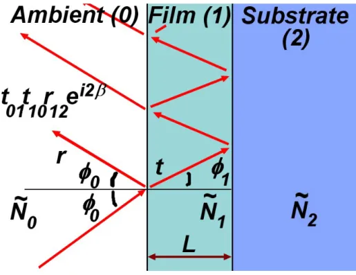
The simple case of a film on a substrate is shown in Fig.4 where L represents the thickness and Ñ the complex refractive index (Ñ=n+ik). Ñ is composed by n, the refractive
Fig. 4: Scheme of a reflected beam (under an incident angle φ0) on a substrate covered with a layer (with a thickness L). Ñj are the complex refractive index and r and t the Fresnel reflection and transmission coefficients.
index of the medium, which is defined by c, the speed of light in vacuum, divided by v, the speed of light in the medium, (n=c/v). Its imaginary part, k, is related to α the absorption coefficient of the medium for a certain wavelength λ. ( αλπ
4 =
k ).
We notice here that with these optical parameters, the dielectric function ε of the medium can also be expressed.
ε=ε1 + iε2 (ε1 the real part and ε2 the imaginary part of the dielectric function)
Ѳ= εμ (but in this case (non magnetic material) μr is very close to 1 in optical frequency)
ε = Ñ2
= (n+ik)² ε1 = n2 – k2
ε2 = 2nk
Using the Fresnel equations, rs and rp can be written:
1 1 ~ 0 0 ~ 1 1 ~ 0 0 ~
cos
cos
cos
cos
φ
φ
φ
φ
N
N
N
N
r
s+
−
=
(7) 1 0 ~ 0 1 ~ 1 0 ~ 0 1 ~cos
cos
cos
cos
φ
φ
φ
φ
N
N
N
N
r
p+
−
=
(8)The reflection coefficient ρ can then be expressed as a function of all the parameters.
)
,
,...
,...,
,
,
(
2 0 ~ 1 ~ 0 ~λ
φ
ρ
ρ
=
N
N
N
L
(9)Several terms in the equations like φ0 the angle of incidence or λ the wavelength are
already known. The only parameters determinable by an ellipsometric measurement are Ψ and Δ. This means that only two unknown parameters can be worked out. For complex systems a simulation using a model of the optical system used is necessary. In such systems the values of the parameters measured by the ellipsometer (ψ and Δ) are calculated and the different parameters are fitted until the calculated values give a result as near as possible to the measured one. In order to improve the accuracy of the approximation, measurements have to be made on a large wavelength scale.
In the case of absorption, the matter is modified. These effects will be used in photo-electric devices (Solar cell) for example. They are based on the energy of the incoming photon.
Regarding the photo-electric devices, three interactions are important:
- The absorption, a photon can be absorbed, i.e. it will give its energy to an electron of the valence band and this one will be excited into the conduction band.
- The emission, a photon is emitted when an electron fall from the conduction band to the valence band.
- The stimulated emission, an incident photon will perturb an electron of the conduction band, this electron will fall to the valence band and emit a photon with the same phase, direction, polarization and frequency than the incoming one. The incoming photon will not be destroyed during this process.
If a photon with an energy higher than the band gap hits an electron in the valence band of the semiconductor, the photon will give its energy to the electron which will be excited into the conduction band. This means that it will have an electron in the conduction band (which can move inside the crystal) and a hole in the valence band (which can also move inside the crystal).
If nothing is done, the electron will lose energy (by emitting a photon or by transferring kinetic energy to the system) and go back into the valence band (recombination). The probability of recombination increases if there is energy level in the band gap due to defects. This is why it is important to have a very pure material (99.9999%). More
Fig. 5 : Scheme of a band structure in a direct semi conductor. After receiving enough energy from a photon, an electron (black spot) moves to the conduction band and lets an empty place (white spot) called hole in the valence band.
information about the losses will be given in the section 2.6.3 losses of the solar cell sub-chapter.
The number of charge-carriers generated under illumination can be described by a generation function G(x,t) which can be expressed as the product of a time dependent function f(t) representing the temporal profile of the excitation and a spatial dependent function g(x) reflecting the spatial profile of the generation given by Beers´ law:
G(x,t)=f(t)g(x) (10)
An equal concentration of mobile electrons (Δn0(t)) and holes (Δp0(t)) are generated if
the energy of the incoming light is higher than the band gap. As the quantum efficiency for generation can assumed to be unity for semiconductors, g(x) and so the density of electron-hole pairs generated by monochromatic excitation light of wavelength λ, absorption coefficient αλ and photon density Iλ is given by:
Δn0(t)= Δp0(t)=(1-R)f(t)Iλαλe-αx (11)
Where (1-R) takes reflection of the incoming light into account.
For the measurement of the temporal evolution of the photoinduced excess charge-carriers techniques such as Time Resolved Microwave Conductivity used to determine lifetime. The mode of generation of charge-carriers is essential for the meaning of the results. This is why several modes of optical excitation characterized by different shapes for f(t) can be distinguished:
1. Stationary (steady state) excitation. Measurements under stationary excitation will be called Steady State PhotoConductance (SSPC) measurements.
2. Pulsed excitation. Transient measurement under pulsed excitation will be called Time Resolved PhotoConductance (TRPC) measurements.
3. Quasi steady state excitation. These measurements will be called Quasi-Steady-State Photoconductance (QSSPC) measurements [II.4].
4. Harmonically modulated excitation. These measurements will be called HMPC measurements [II.5].
All excitation modes can be used under bias illumination: a constant illumination but with much higher intensity as the modulation light is simultaneously applied.
Further explanations about the kinetics of the generated excess charge-carriers will be discussed in the section 2.3. Charge-carriers kinetic
To avoid the phenomenon of recombination, besides using very pure silicon, the charge-carriers (i.e. the electrons and the holes) have to be separated. If the semiconductor is then connected to an external circuit, the generated “excess” charge-carriers can contribute to the supply of an electric load. The typical way to reach that goal in the silicon solar cell is to use a “p-n” junction.
2.2. Junctions
A junction is prepared when two materials with different properties are brought together to establish a junction in the semiconductor device sense (physisorption or chemisorption are necessary). In the case of the p-n junction, the base material is always the silicon (in the case of this work), only its doping is changing, forming a so called homojunction. First of all we have to introduce the notion of dopant. Let us take, for example, a crystalline lattice of silicon (column IV in the periodic table of the elements) and replace some of the silicon atoms with phosphorus atoms. The Phosphor (column V) has 5 valence electrons and 4 of these will bond to the surrounding silicon to form the crystalline lattice. The 5th electron, due to the thermal excitation, will be donated into the conduction band. Consequently, the Phosphor will have an extra positive charge. Phosphor is called a “donor” because it gives one electron to the conduction band and this then leads to a n-type doped silicon. The same principle is applied to atoms (such as boron) which have one less electron. The atom of Boron will take an electron of a neighboring Si-Si bond (an electron of the valence band) to build its own bonding with the 4 atoms of silicon around it. Because of the strong bonding energy this electron will no longer be able to move (contrary to the hole generated) and thus it will give a negative ion. Such atoms are called “acceptors” and the result is p-type doped silicon.
A p-n junction is realized when 2 semiconductors, a p type and an n-type one are in contact. In the case of silicon solar cells, both semiconductors are silicon and the dopants used are usually Phosphor and Boron. The concentration of acceptors will be called Na and the
concentration of donor Nd. The density of electrons will be named n and p the density of
fig. 6 : On the upper part, the scheme of a p-n junction. The space charge region has a width between 0, 1 and 1 μm. On the lower part, the band diagram resulting of the junction between 2 pieces of silicon. One p doped (right side of the junction) and one n doped (left side of the junction). The junction itself take place at the thickness 1. This graph was obtained with the software AFORS HET. The blue line is the energy of the valence band, the red one the energy of the conduction band and the green one is the Fermi level.
When a p and an n type piece of silicon are brought together, the excess of electrons in the n semiconductor will diffuse to the p region and recombine with the holes. The holes in excess in the p region will follow the opposite direction. At the interface, a region will be created where donors and acceptors are no longer neutralized.
The recombination of free charge-carriers on both sides of the junction and thus the resulting ionized donors and acceptors will generate a space charge. Therefore, at the
metallurgical interface, an electric field E will act against the diffusion of the majority → carriers and when this field is equal to the diffusion force due to the free charge-carriers concentration gradients, the thermodynamic equilibrium is then obtained.
When a photon (with an energy higher than the band gap) hits the semiconductor, it will generate an electron-hole pair. Three cases are possible: The pair is generated in the p type region, in the space charge region or in the n type region. As previously mentioned, an electric field in the space charge region prevents the majority charge-carriers from crossing this region, but not the minority carriers. This means that the electron-hole pairs will diffuse in p and n type, when they attain the space charge region, the minority charge-carriers will be injected into the region where they are the majority carriers. In the space charge region, because of the electric field, electron-hole pairs will be separated, the holes will be injected into the p region and the electrons into the n region.
In a silicon solar cell, the p-n junction plays an important role. One of the biggest challenges is not to generate electron-hole pairs under illumination, but to separate them completely in order to use ideally all of them to drive a load.
Fig. 7 : When a photon generates charge carriers in the silicon, the holes and electrons produced will be separate as shown on this picture.
2.3. Charge-carrier kinetics
As seen previously, the excitation (under illumination) of a semiconductor leads to a generation of excess charge-carriers. These charge-carriers are not static inside the semiconductor and in this section we will speak about their kinetics. Before discussing about the kinetics of the charge-carriers let us assume that the system is one-dimensional where the thickness d is the only relevant parameter (x-direction) and the system is homogeneous in the y/z direction. The system is also assumed to be homogeneous in the x-direction with the exception of an infinitely thin range at both surfaces characterized by a different structure (in particular defect density). Only electrons at the bottom of the conduction band and holes at the top of the valence band are mobile charge-carriers and contribute to the (photo)conductance in c-Si. Excess charge-carrier dynamics is described with the drift diffusion model [II.6]. This model is generally used for semiconductor device simulation and is sufficiently sophisticated for our purposes if degeneration is avoided or taken into account in a restricted range. Furthermore, it is assumed that no applied field is present. To obtain an overview of the kinetics we used the photoconductance ΔP. This value is obtained by the following equation (12). It is composed by Δn, the excess electron concentration with a mobility μn at the bottom of the conduction band and Δp, the excess hole concentration with a
mobility μp at the top of the valence band:
dx e x p e x n P p d n ( ) ) ) ( ( 0 μ μ +Δ Δ = Δ
∫
(12)Eq.(12) shows that ΔP reflects the number of excess charge-carriers weighted by the mobilities. For the different excitation modes (seen in sub-chapter 2.1.2 Interaction light -
matter) there is a dependence of ΔP and the excess charge-carrier concentrations on time t
since the start of the excitation (for pulsed excitation) or modulation frequency ω (for harmonically modulated measurements). For all excitation modes ΔP can be measured as a function of the excitation density.
Two kinds of information can be obtained from ΔP:
-The mobility of excess charge-carriers if their number is known. -The kinetics of excess charge-carriers.
An effective lifetime τeff (of the excess charge-carriers) can be determined from the
experimental ΔP(t) transient. This leads to following definitions for the different excitation modes (2.1.2 Interaction light - matter):
-For stationary excitation:
(
)
e N P p n ss ss eff μ μ τ + Δ Δ = 0 (13)where ΔPss refers to the photoconductance under stationary illumination and ΔN
0 to the
number of holes (which is equal to the number of electrons under the excitation conditions defined above) generated by the illumination.
-For pulsed excitation:
( )
(
)
( )
t( )
t P t P t tr eff ∂ Δ ∂ Δ − = 1 1 τ (14)Where the time t refers to the time passed since the start of the illumination. Short laser pulses (10ns FWHM) are frequently used and in many cases the duration of the illumination can be neglected relative to the time constants of the relevant kinetic processes (δ-function excitation)
-For quasi-steady-state illumination
Here the sample is illuminated by a relatively long light pulse (in the ms range). In many cases the decay time of the illumination is much longer than all kinetic processes of interest. Then τeffqss is defined as for stationary illumination (Eq.13) but a more general
definition can be used [II.7].
-For harmonic modulation [II.5, 8]:
2 ) ( 1 ) 0 ( ) ( hm eff P P ωτ ω ω + = Δ = Δ (15)
Where ΔP(ω) refers to the modulus of the photoconductance induced by harmonically modulated illumination at modulation (angular) frequency ω. These effective lifetimes refer to the time passed by excess charge-carriers in the conductive state (at the bottom of conduction band for electrons and the top of the valence band for holes) before being immobilized (due to trapping or recombination). These lifetimes can be a function of time (for transient measurements induced by pulsed excitation), excess carrier densities and profiles. Because
these parameters are different for the excitation modes, also τeff determined is in general
different.
Within the model used here τeff is due to 3 decay processes, if trapping is neglected:
- Recombination in the volume characterized by τv
- Recombination at the front surface (illuminated surface) characterized by τsfr
- Recombination at the back surface characterized by τsba
The effective lifetime can be considered as a parallel combination of these recombination times: fr s ba v eff τ τs τ τ 1 1 1 1 + + = (16)
Eq.16 is not particularly useful because the contribution of the different decay processes to τeff is not clear before a more detailed study of kinetics is done. However, in the
present model τsfrand ba s
τ depend on the thickness d of the sample (Eq. 34, 36) whereas τv does not. The contribution of surface recombination to the total decay can be enhanced by the use of light with a high absorption coefficient, i.e. surface excitation and minimized by the use of light with a low absorption coefficient, i.e. volume excitation. The surface recombination will be treated more in detail in the following sub chapter 2.4 Passivation.
If the surface recombination can be neglected, the effective lifetime depends only on τv. In this case if τv is constant (i.e. depends neither on the injection level nor on time) all
excitation modes yield the same effective lifetime identical to τv.
After this general introduction, the following text will deal with the charge-carrier kinetics in the case of a transient measurement (TRPC), i.e. pulsed excitation generation. The conversion to the other generation modes is trivial or, when important, indicated.
Under the conditions given above the concentration of excess charge-carriers is described by the 2 continuity equations, one for electrons and one for holes, and the Poisson equation relating these 2 equations, if no external field is applied. The continuity equation for the excess electrons is given by:
) , ( ) , ( ) , ( 1 ) , ( t x G t x R x t x j q t t x n n n − + ∂ ∂ = ∂ Δ ∂ , (17)
and for excess holes: ) , ( ) , ( ) , ( 1 ) , ( t x G t x R x t x j q t t x p p p − + ∂ ∂ − = ∂ Δ ∂ . (18)
With the following expressions for the currents jn and jp:
x t x n qD t x E t x n q t x jn n n ∂ ∂ + = ( , ) ( , ) ( , ) ) , ( μ , (19) and x t x p qD t x E t x p q t x jp p p ∂ ∂ − = ( , ) ( , ) ( , ) ) , ( μ , (20) this yields:
( ) ( )
(
)
) , ( ) , ( ) , ( , , ) , ( 2 2 t x G t x R x t x n D x t x E t x n t t x n n n n ⎟⎟− + ⎠ ⎞ ⎜⎜ ⎝ ⎛ ∂ Δ ∂ + ∂ Δ ∂ = ∂ Δ ∂ μ (21) and( ) ( )
(
)
) , ( ) , ( ) , ( , , ) , ( 2 2 t x G t x R x t x p D x t x E t x p t t x p p p p ⎟⎟− + ⎠ ⎞ ⎜⎜ ⎝ ⎛ ∂ Δ ∂ + ∂ Δ ∂ − = ∂ Δ ∂ μ , (22)with Dn (Dp) the diffusion constant of electrons (holes), n(x,t)(p(x,t)) the total
concentration of electrons (holes), Δn(x,t)(Δp(x,t)) the concentration of excess electrons (excess holes) , μn (μp) the mobility of electrons (holes), Rn (Rp) the decay function of
electrons (holes), E the (internal electric field built up by the differing transport velocity of electrons and holes) and G the generation function (equal for electrons and holes).
The decay function R represents all the processes leading to immobilization (i.e. trapping, recombination) of the corresponding species. As mentioned above, the generation function G(x,t) (which represents the generation of excess charge-carriers) is identical for electrons and holes. These two equations are connected by the Poisson equation:
(
a d)
r N N t x p t x n q t x E = − + + − Δ ( , ) ( , ) ( , ) 0ε ε (23)With q the unity charge, ε0εr the dielectric constant and Na(Nd) the concentration of
ionized donors (acceptors).
Most important for our purpose is the decay function R: in the general case it involves the 3 decay mechanisms relevant in Si [II.4, 9, 10]:
- Bimolecular radiative recombination - Auger recombination
The Auger recombination and the bimolecular recombination will not be discussed here as they occur at high injection which is not relevant to our case. However, more information about them can be found here [II.11, 12] The recombination via defects (or Shockley-Read-Hall (SRH) recombination) reflects the interaction between mobile charge-carriers in the bands and lattice defects [II.13, 14].
A lifetime τn (τp) for electrons (holes) can be introduced by the definitions:
Rn(t) = Δn/ τn (24)
and
Rp(t) = Δp/ τp (25)
It is clear that in the general case τn and τp depend on all the parameters of the system,
i.e. time t, coordinate x and the local densities Δn(x.t) and Δp(x,t). In the case of SRH recombination the lifetimes depend also on the density of recombination centres and the corresponding cross sections.
For the solution of the Eqs.21-23 the appropriate boundary conditions must be chosen for n, p and E at every surface [II.15, 16].
The model for excess charge-carrier kinetics described by Eqs.21-23 and the boundary conditions will be called the extended kinetic model. For evaluation of PhotoConductance data with the extended kinetic model the solution of Eq.(21,22), i.e. Δn(x,t), Δp(x,t) must be integrated over the thickness of the sample as ΔP refers to the integral number of excess charge-carriers (Eq.12).
The complexity of the extended kinetic model limits its usefulness. Applications seem to be limited to determination of the parameters that yield the best fit of experimental data to the model [II.15, 16].
The theory can be greatly simplified if quasi-neutrality is assumed:
Space charge is neutralized with a characteristic time, the dielectric relaxation time,
given by εσ0εr , that can be assumed to be infinitely short relative to the relevant time scale of the measurements. This yields Δn(t)= Δp(t) and under some generally acceptable
ambipolar diffusion equation. In this model excess charge-carriers diffuse as electron hole pairs and so neutrality is maintained. More details on this model can be found in textbooks [II.17-II.19].
Transport in a (quasi)neutral region can be described by the ambipolar diffusion equation: ) , ( ) , ( ) , ( ) , ( 2 2 t x G t x R x t x n D t t x n n + − ⎟⎟ ⎠ ⎞ ⎜⎜ ⎝ ⎛ ∂ Δ ∂ = ∂ Δ ∂ , (26)
where D refers to the ambipolar diffusion constant:
p n p n pD nD D D p n D + + = ( ) . (27)
Under low injection conditions (Δn=Δp<<n+p) D reduces to the minority carrier diffusion constant. This has lead to the convention to associate Eq.27 to the minority carriers
In this model the number of boundary conditions is reduced to two: one condition at every surface given by application of the continuity equation to both surfaces:
) ( ) , ( 0 t R x t x n D = sfr ∂ Δ ∂ (28) and ) ( ) , ( t R x t x n D sba d = ∂ Δ ∂ (29),
with R the surface recombination rate at the front side (at x=0) andsfr ba s
R the surface
recombination rate at the back side (x=d).
The conventional approximation is that the recombination processes are first order, i.e. proportional to the excess minority carrier concentration Δn(x,t), this gives:
v n t x n t x R τ ) , ( ) , ( = Δ (30)
with τv the (minority) volume lifetime and for the surfaces:
) , 0 (x t n S R fr fr s = Δ = (31)
) , (x d t n S Rsba = baΔ = (32)
Where Sfr and Sba are the surface recombination velocities (in cms-1) at the front and
the back side, respectively.
The standard description of PC measurements is with Eq.(26) ,boundary conditions Eqs.28-29 and also the approximations of Eqs.(30-32) . This will be called the simple kinetic model. It explains satisfactorily many experimental results for c-Si and somewhat less satisfactorily for mc-Si.
Analytical results for the simple model have been determined for δ-pulse with the time profile of the laser pulse (g(x)) as an initial condition [II.20]. For evaluation of PC data with the simple kinetic model the solution of Eq.(26), i.e. Δn(x,t), must be integrated over the thickness of the sample as ΔP refers to the integral number of excess charge-carriers (Eq.12).
Although it is recommendable to solve Eq.26 numerically where also the time profile of the excitation can additionally be taken into account [II.20], an interesting conclusion can be drawn from the analytical solution [II.21]. Indeed, the decay of the excess charge-carrier distribution occurs via modes with different decay times. These modes correspond to the Fourier components of the initial distribution of excess charge-carriers as determined by the distribution generated by the excitation light (Eq.11). The mode with the longest decay time is called the principal mode.
This is particularly interesting for TRPC measurements where the final decay (within the simple model represented by an exponential decay) is from this quasi stationary principal mode. It is intuitively clear that the surface decay time, τs, of this principal mode depends on
the surface decay rate and the velocity of the supply of excess charge-carriers by diffusion. The two extreme cases are given for TRPC measurements by [II.22, 23]:
− For S very large 2 2 1 d D s π τ = (33) and so 2 2 1 1 d D v π τ τ = + (34)
Where τ refers to the total decay time of the principal mode.
The distribution of excess charge-carriers corresponding to this decay time is half a sinus-wave with the excess charge concentration effectively zeros at the surfaces. This case can be
called diffusion controlled surface recombination because 1/τs is determined by the supply of
excess (minority) carriers to the surfaces. Here the surface recombination rate is at its maximum level. − For S small d S s 2 1 = τ (35) and so d S v 2 1 1 = + τ τ (36)
The distribution of excess charge-carriers corresponding to this case is a uniform distribution. This case can be called rate limited surface recombination because 1/τs is
determined by the surface decay rate and the supply of excess charge-carriers to the surfaces is sufficiently fast enough to flatten the distribution at any time. A problem of the analytical solution of Eq.26 is that the faster decaying modes must be considered together for an interpretation of the decay behaviour and the excess charge-carrier distribution. Consequently, interpretation of the initial decay is more convenient by a numerical solution.
2.4. Passivation
The passivation, of a solar cell can have different meanings: chemical passivation and electrical passivation. The first one should protect the cell from impurities providing a coating able to prevent degradations from the environment. The second one have to reduces losses due to recombination (in the bulk or at the surface) [II.24, 25]. This work focuses on the electrical passivation only.
Thanks to the progression of technology used to make crystalline silicon, very pure silicon (99.9999% for the standard solar quality and even 99.99999999% for the electronic quality) is now available. This means that for a cell several hundred micrometers thick, we are able to neglect the recombination in the bulk because the charge-carriers generated in the silicon have the time to attain the surface before they recombine. This is why the surface passivation has an important place in the conception of high efficiency silicon solar cells. This work will focus specifically on the silicon nitride whilst additionally comparing it with the amorphous silicon and the silicon oxide which passivate the surface of a silicon wafer.
The recombination is generally due to energy states within the band gap (for example, due to a defects). At the surface two other phenomena, an intrinsic and an extrinsic one, are creating localized states in the band gap. The first one is due to the end of the lattice where the atoms at the interface are not bonding with theirs neighbours like the ones in the bulk. They are only bonding in a half plane and are thus called dangling bonds. This electronic configuration will modify the band diagram and generate energy states in the band gap. The second phenomena is due to impurities (other atoms from those which make up the semiconductor, like oxygen) which are present at the surface. Those atoms will modify the electronic structure (introduce energy states in the band gap) and they will also create distortions in the lattice which will give recombination centres.
To minimize the recombination at the surface and thus the surface recombination velocity, there are several possible solutions. A surface field can be generated in order to push back into the bulk one type of charge-carriers (and thus reduce the possibility of recombination). Another possibility would be the deposition of a layer on the top of the semiconductor to suppress the dangling bonds.
One of the first surface passivation techniques was the growth of a thermal oxide layer on the silicon substrate. The oxide is formed at high temperatures (around 1000°C) and during the process the silicon oxide layer grows into the silicon substrate. This will move the
interface silicon-oxide / silicon into the bulk of the substrate. By chemically bonding to silicon atoms, the oxygen atoms will suppress (or significantly reduce) the dangling bonds and hence reduce the recombination at the surface. The production of those oxide layers is highly reproducible and a good passivation is obtained. With a refractive index of 1.5 (lying between the silicon’s one (nSi=4) and the air’s one (nAir=1)), the silicon oxide can also act as
an anti-reflection coating.
However the silicon oxide layer has also some disadvantages. • The cost of energy used to build this film.
• The possible contamination by diffusion of impurities during the process. • The degradation of lower quality Si-wafer.
For these reasons it is preferable to work with coatings made at lower temperature.
The amorphous hydrogenated silicon nitride (designated by SiNx in this work) seems
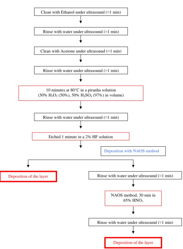
to be a good alternative to silicon oxide as a passivation and anti-reflection coating for silicon solar cells. We will study SiNx deposited as described in the sub chapter 4.1 Deposition’s
methods. The low temperature deposition minimized the contamination and varying parameters allowed us to form different silicon nitrides (by the composition, density …). Another possibility for a good passivation is the amorphous silicon which is also deposited at low temperature but its high refractive index and its high absorption make its use as a front coating less useful.
2.5. Anti-reflection coatings
The silicon solar cells are based on a silicon substrate (mono-crystalline, multi-crystalline, etc…). To maximize the generation of excess charge-carriers, the number of photons which can be absorbed must also be maximized. The silicon has a band gap of 1.12 eV and following the Lambert-Beer’s law mostly all photons with an energy higher than the band gap will generate charge-carriers. The conversion between energy and wavelength is described by the following formula:
meter Joule
h
c
E
λ
*
=
or for practical use:m eV
E
μλ
24
.
1
=
(37)Where E is the energy of the photon (in Joule or eV), c the speed of light, h the Planck’s constant and λ the wavelength (in meter or micro meter).
As shown on the transmission spectrum of a p type piece of silicon every photon with a wavelength under 1100 nm is absorbed (or reflected)
A non negligible optical loss process with silicon (in silicon solar cells) is its high reflection [II.26], especially in the visible range of the light, where the maximum of the sun light intensity takes place (around 500 nm). This effect is due to its high refractive index, around 4.32 for a radiation of 500 nm [II.1]. Under a perpendicular incidence, the intensity of the light which is reflected at the interface between 2 different media, is given by the
Fig. 8 : Transmission of a p type, 500 μm thick silicon substrate as a function of the wavelength. With a band gap of 1.12 eV and following the Beer-Lambert law, mostly all photons with a wavelength under 1100 nm are absorbed. The graph shows only the photons passing through the sample (related with the incident beam)
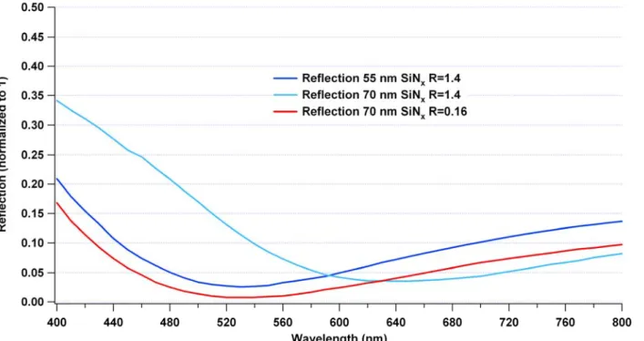
Fig. 9 : Reflection of a silicon substrate as a function of the wavelength between 400nm and 800 nm. The maximum of the sun light intensity is located around 500 nm, which shows clearly the need of an anti-reflection coating to reduce the losses.
reflection coefficient R expressed by the following formula (deduced from the Fresnel equations). The coefficient R also has a component on the plan parallel to the plan of incidence (Rp) and another one perpendicular to this plan of incidence (Rs).
Considering Eq. 7, 8 (2.1.2 Interaction light – matter) the total reflection coefficient R is defined by:
2
s pR
R
R
=
+
(38) With: 2 p pr
R
=
(39) 2 s sr
R
=
(40)Thus, for a normal incidence of the beam (φ0 = 0°) and a non absorbing layer (k=0):
2 2 1 2 1
⎟⎟
⎠
⎞
⎜⎜
⎝
⎛
+
−
=
=
=
n
n
n
n
R
R
R
p s (41)At the interface between air (n1=1) and silicon (n2=4.32 for λ=500nm) the reflection
should be around 0.39. It means that 39% of the incoming light with a wavelength of 500 nm will be reflected. An anti-reflection coating (ARC) is therefore necessary to reduce these huge losses due to reflection.
The anti-reflection effect can be performed thanks to the deposition of a thin layer between the 2 media (air and silicon in this case).
The best refractive index n1 for an anti-reflection coating between the 2 media with
respectively a refractive index n0 and n2 can be deduced from the formula:
2 0
1 n n
n = . (42)
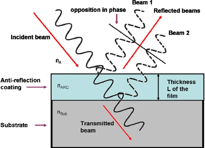
An anti-reflection coating uses the interference properties to reduce the reflection. Indeed, if for a perpendicular incidence, the film has a thickness equal to the quarter of the wavelength in the film (this wavelength is defined on p. 30). The reflected beam and the incident one will be exactly opposite in phase. If both intensities are equal, both beams will interfere destructively one with each other. This will suppress the reflection for the selected wavelength.
Fig. 10: Scheme of the simple reflection of a beam of light at the interface between 2 media with different refractive index. The light blue square represents an anti-reflection coating with a refractive index n1 such as n0< n1<n2
Fig. 11: Scheme of the destructing interference process (the proportions are not respected). The beams reflected at the interface Air-Anti reflection coating (beam 1) and the reflection at the interface anti reflection coating – substrate are opposite in phase. This leads to a destructive interference and all the energy of the incoming beam is transmitted into the substrate. For simplicity, no refraction of the transmitted beam is shown.
The amplitude of the reflection coefficients at both interfaces are:
ARC A ARC A ARC A
n
n
n
n
r
+
−
=
− (43) Sub ARC Sub ARC Sub ARCn
n
n
n
r
+
−
=
− (44)The complex reflection coefficient between the ambient and the substrate is:
Sub ARC ARC A i Sub ARC ARC A Sub A
r
r
e
r
r
r
− − − − − −+
+
=
1
ϕ (45)Where ϕ is the phase shift introduced by the Anti-reflection coating. λ
πδ
ϕ = 2 with δ the path difference (δ=2nSub.dSub/cosφ1 , φ1 the angle of the transmitted beam with the normal after the interface Ambient-ARC )
A wavelength changes when it goes from one medium to another. This means that in order to calculate the appropriate thickness of the anti-reflection coating, the refractive index must be taken into account. The optimum thickness for destructive interferences can be determined by the formula λ0/(4*n) with λ0 the wavelength in vacuum and n the refractive index of the medium. In the case of silicon nitride the perfect thickness to suppress the reflection at the wavelength of 532, for example, is 532/(4*1.9)=70 nm.
To calculate the anti-reflection, a software taking the multiples reflections and the absorption of the layers into account was programmed. More details are given in the section
2.6. Solar cells
Crystalline Silicon solar cells are the most common type of solar cells, they represent more than 90% of the photovoltaic market. They can be found in different form:
- The mono-crystalline silicon solar cell is the most efficient (22.3% for HIT cells and up to 24.7% for the best p-n junction solar cell [II.27]). But these record cells are manufactured with a very expensive process.
- The multi-crystalline silicon solar cell is the standard for commercial application, it is cheaper compared to mono-crystalline cells but the efficiency is lower (between 15.3% to maximum 20.3%).
- We can also find multi-crystalline silicon solar cells based on silicon ribbon [II.28] sheet which also have a lower efficiency than the mono-crystalline cells but the fabrication process does not need to saw ingots and therefore the waste of silicon is reduced.
This work will focus on the standard crystalline silicon solar cell, based on a crystalline silicon substrate with electric contacts on the front and back side. Firstly we will examine the conventional silicon solar cell with its different aspects. Following on from this we will look at the concept of the inverted solar cell and the advantages of the new geometry used will be shown.
2.6.1. Principle of a p-n junction crystalline silicon solar cell
In a semi conductor, like silicon, and without any excitation (T=0K), all the electrons are in the valance band. If we excite the atoms in a crystal with light for example, some photons can transfer their energy to the electrons of the valence band which will be excited into the conduction band (if the energy is higher than the band gap). The generated electrons and the holes have to be separate to contribute to a photovoltage. This separation takes place in the space charge region of a p-n junction.
An n layer is created on a p type silicon substrate by thermal diffusion. A front and a back contact (generally metal is deposited on the surface) for the collection of excess charge-carriers into the external circuit are created. On the front surface a texturing can be performed and an anti-reflection coating can be deposited in order to enhance the light coupling into the absorbing layer.
Fig. 12 : Scheme of a typical silicon solar cell. The substrate is a p-type silicon. The n-type region is created by thermal diffusion of dopands (phosphorus).
2.6.2. Losses
Silicon solar cells do not convert all the energy of the incoming light into electricity. The best silicon solar cells (made in a laboratory) are able to reach 24.7% of efficiency [II.27] (without any focusing system). The limitation of the efficiency is due to the losses of energy. The losses have several origins [II.26], they can be optical, energetic or structural. In the Fig.13 you can see a scheme of the optical and energy losses.
The optical losses can have two reasons. One occurs from photons which are reflected at the cell surface (red line), it concerns around 35% of the photons with a wavelength of 500 nm coming onto crystalline silicon without any anti-reflection coating. Other losses come from photons which will pass through the cell without being absorbed, indeed, photons with energy lower than the band gap of the silicon will not have enough energy to excite an electron of the valence band into the conduction band. If we take the case of silicon with a
band gap of E=1.12 eV the associated wavelength is λ E 1,12 1,107μm 24 , 1 24 , 1 = = = it means that
photons with a wavelength higher than 1100 nm will mostly not be absorbed (blue line on the Fig.13).
The energy losses come from the interaction of the incoming photons and the matter. In fact, the photons emitted by the sun have different energies. The solar cells use the light coming from the sun, either in space or on earth. In both cases the spectrum of the incoming light covers a very large wavelength range, as shown in Fig.14.
Fig. 13 : Energy losses (i.e. difference between the incoming energy of the incident light and the energy finally turned into electric energy) occurring in a semi conductor when it is illuminated.
The photons with energies higher than the band gap can create electron-hole pairs, but it is necessary to take into account several possible cases:
- The photon can give the energy of the band gap to the electron. In this case the electron-hole pair generated can sometime recombine (directly or though defects) before they can be injected into the external circuit (orange line).
- Another loss of energy due to these high energy photons can be the thermalisation. In this case, the photon gives more energy to the electron than the band gap. The electron (hole) pair generated will have to lose some energy to reach the lower (higher) part of the conduction (valance) band (green line).
- Another source of losses comes from the thickness of the cell. Even if the energy of the incoming photon is high enough, they can pass through the cell without being absorbed. These losses can be reduced by a back surface reflection for example.
These losses are taking into account the processes acting on the generated charge-carriers. Indeed, excess charge-carriers can be trapped or they can recombine. This is due to the presence of defects in the bulk or at the surface. Defects induce sub-energy levels in the
Fig. 14 : Spectrum of the irradiance [II.29] of the sun light. The difference between the irradiance outside atmosphere and at the sea level is due to the absorption (by CO2, H2O etc…) in the atmosphere.
forbidden band gap, hence, it is more probable for charge-carrier pairs to recombine. Defects in the bulk can be due to a stacking fault in the lattice or impurities present in the silicon (related to the kind of silicon used). Amorphous silicon only contains defects because of its amorphous composition. The multi-crystalline silicon consists of large grained crystallites (the defects take place between the grains of silicon). The silicon with lowest defect density is the mono-crystalline one, but even in the best quality crystals impurities can be found or some stacking faults in the crystalline lattice can occur.
The engineering process, such as the shadowing of the cell by the front contact, can cause other additional losses.
Fig. 15 : Scheme of an inverted silicon solar cell. The bulk is a n-type piece of silicon. The junction is made by deposition of a p-type amorphous silicon.
2.6.3. Motivation for the inverted geometry silicon solar cells
One problem of cells based on thermal diffusion of the p-n junction is that it requires a lot of energy because the wafer must be heated up to 1000 degrees Celsius. It costs a lot of energy/money and the risk to include impurities by this method is also higher. A deposition made at low temperature would be favourable to reduce costs. A part of the problem was solved by the deposition of doped amorphous silicon in order to have a p-n junction at low temperature, but the absorption in this dead layer is still a problem. All the excess charge-carriers generated in this area are lost due to their poor lifetime in this high defect region. This is also the case of the photons in the blue range of the solar spectrum for example (
α
400=95200 cm-1) which are an important part of the sun light.To pass through these problems, another kind of solar cell is proposed, still based on crystalline silicon but using another geometry, the “inverted a-Si:H/c-Si heterocontact solar cell” [II.30].
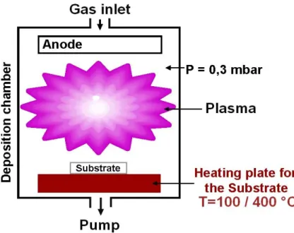
In this kind of cell the p-n junction is placed on the back side. The junction is made by deposition at low temperature (250°C) of a p a-Si:H on a n c-Si substrate by Plasma Enhance Chemical Vapour Deposition (PECVD), this avoids the problem of the high temperature process. Absorption due to the hetero junction is then drastically reduced.
3. Methods
The studied layers (silicon nitride, amorphous silicon and silicon oxide) have different characteristics and properties. A modification inside the layer can modify its characteristics and behaviour, which is why a good investigation of the coatings by different aspects is necessary. Consequently, several methods were used to analyze these coatings. This chapter will describe the measurement methods used, explain their principles and show the kind of information we can obtain. The analysis of the data and their interconnection with each other will be presented in chapter 4. Coatings on silicon substrates. The characterization of the different material properties can be divided in 3 parts:
1. The optical characterization: to determine the optical parameters or the anti reflection properties of the layer.
2. The electrical characterization: used to obtain the passivation properties (surface and bulk) of the layer and the fixed charge in the film.
3. The structural characterization: to know the composition and the structure of the coating.
3.1. Optical characterization
This sub-chapter will give an introduction to the different experiments used to analyze the optical properties of the layers.
3.1.1 Ellipsometry
Ellipsometric measurements allow us to obtain the optical properties of a layer (refractive index, absorption) and also its thickness. The ellipsometric measurements were performed at the University of Metz (France), by doctor En Naciri. Some other measurements with a monochromatic ellipsometer were made at the H.M.I. The ellipsometer used at the University of Metz uses a spectral source which allows us, compared to monochromatic ellipsometer, to have the refractive index (but also the other optical parameters) over a wide range of wavelengths.
Ellipsometry is an optical technique using the vectorial nature of an electromagnetic field. The reflection on the sample will induce modification of the polarization of an incoming (polarized) light. As shown in the sub-chapter 2.1.2 Interaction light-matter
Fig. 16 : Scheme of the PRPSE ellipsometer used at the University of Metz to do the ellipsometric measurements. The Xeon lamp is the light source and PM the photomultiplier which will count the photons of each wavelength coming onto it. The first polarizer is fixed, it polarizes linearly the incoming light and suppresses the residual polarization of the source.