Design of Miniaturized Radio-Frequency DC-DC
Power Converters
. by
Anthony D. Sagneri
B.S., Rensselaer Polytechnic Institute (1999)
S.M., Massachusetts Institue of Technology (2007)
Submitted to the Department of Electrical Engineering and Computer Science in partial fulfillment of the requirements for the degree of
Doctor of Philosophy
MAat the
MASSACHUSETTS INSTITUTE OF TECHNOLOGY
February 2012@
Massachusetts Institute of Technology, MMXII. All rights reserved.SSACHUSETTS INSTflWTE OF TECHNOLOGY
MAR20 2012
LIBRARIES
ARCHIVES
AuthorDepartment of Electrical Enfeering and Computer Science January 13, 2012
Certified by -
7
David J. Perreault Professor, Department of Electrical Engineering and Computer Science Thesis Supervisor
Accepted by
I \"L esli o4 . * ol odziejski Chairman, Departmental Committee on Graduate Students
Design of Miniaturized Radio-Frequency DC-DC Power Converters
by
Anthony D. Sagneri
Submitted to the Department of Electrical Engineering and Computer Science on January 13, 2012, in partial fulfillment of the
requirements for the degree of Doctor of Philosophy
Abstract
P
OWER electronics appear in nearly every piece of modern electronic hardware,forming an essential conduit from electrical source to load. Portable electronics, an area where a premium is placed on size, weight, and cost, are driving the development of power systems with greater density and better manufacturability. This motivates a push to higher switching frequencies enabling smaller passive components and better integration. To realize these goals this thesis explores devices, circuits, and passives capable of operating efficiently into the VHF regime (30-300 MHz) and their integration into power electronic systems of high power density.
A good integrated power MOSFET presages high-density converters. Previous VHF systems were demonstrated with bulky and expensive RF Lateral, Double-Diffused MOSFETs (LDMOSFET). We show that through a combination of layout optimization and safe operating area (SOA) extension integrated devices can achieve near-parity performance to their purpose-built RF discrete cousins over the desired operating regime. A layout optimization method demonstrating a 2x reduction in device loss is presented alongside experimental demonstration of SOA extension. Together the methods yield a 3x reduction in loss that bolsters the utility of the typical (and relatively inexpensive) LDMOS IC power process for VHF converters.
Passive component synthesis is addressed in the context of an isolated VHF converter topology. We present a VHF topology where most of the magnetic energy storage is accomplished in a transformer that forms an essential part of the resonant network. The reduced component count aids in man-ufacturability and size, but places difficult requirements on the transformer design. An algorithm for synthesizing small and efficient air-core transformers with a fully-constrained inductance matrix is presented. Planar PCB transformers are fabricated and match the the design specifications to within 15%. They are 94% efficient and have a power density greater than 2kW per cubic inch. To take full advantage of good devices and printed passives, we develop an IC for the isolated converter having optimized power devices, and integrated gate driver, controller, and hotel functions. The chip is assembled into a complete converter system using the transformers and circuits described above. Flip-chip mounting is used to overcome bondwire parasitics, and reduce packaging volume. The final system achieves 75% efficiency at 75 MHz at 6W.
Thesis Supervisor: David J. Perreault
Acknowledgements
First and foremost I thank Prof. Dave Perreault, my thesis advisor, for his guidance, support, and patience over the course of my time at MIT. He's an incredible source of knowledge and a good example to follow. To (Now) Prof. Juan Rivas who's talent and skill are second to none in this most esoteric of disciplines, and who was a friend through all the interesting times: Thank You.
In addition I make a special thanks to my thesis committee: Prof. John Kassakian, Prof. Jeffrey Lang, and Prof. Tomas Palacios for their support, advice, and help along the way.
National Semiconductor deserves a big boost: They sponsored the thesis work contained herein. A particular thanks to Dave Anderson, another incredible source of knowledge and a particular aid when non-technical problems arose. Also, he has a great car.
To Jackie Hu, whom I originally mistook for a big-glasses, big-sweatshirt nerd: You are a great friend who stuck with me through all the muck. It's impossible to express how much that has meant to me. Thank You.
To Grace Cheung, who deserves this separate paragraph more than any other: I'm grateful we crossed paths. The MIT experience would not have been complete without you. Thank You. To George Hwang: You are a unique animal, the fusion of emotion and a determination that you have thus far chosen to point toward engineering to great effect. You have a lot left to do. Thank you for being a great friend and buttress in the stormy times (and the good ones!).
To Jut (Justin Burkhart): Thanks for reminding me that starting a company was why I came to MIT. To Vanessa Green: Thanks for teaching me (however didactically) that trust is the most essential element of entrepreneurship, whether that's trust of self, others, or just the universe.
Other lab folks: (Now) Prof. Yehui Han, (Now) Prof. Robert Pilawa, Olivia Leitermann, Bran(s)don Pierquet, Alex Hayman, Alex Trubisyn (collectively, "The Alexes"), Wei Li, Fergus Hurley Sam Chang, of course Jiankang Wang, Shahriar Khushushahi, Uzoma Orji, Warit Wichakool, you have been a great network of friendship, support, and technical knowledge at various points over the years.
MIT Cycling: Thanks! Couldn't have had more fun on a bike. In particular I want to call out A.J Schrauth, Alex Chaliff, Yuri Matsumoto, Zuzana Trnovcova, Chewie Chew, David Singerman, Zack Labry, and Nick Loomis. You guys made it fun.
I owe the most to my parents: Richard F., and Mary, without whom I wouldn't exist or be where I am. And to my siblings: Kris, Rich, David, and Catherine who have been many things over the years-there's still a lot to discover.
"Nothing in the world can take the place of Persistence.
Tal-ent will not; nothing is more common than unsuccessful men with
talent. Genius will not; unrewarded genius is almost a proverb.
Ed-ucation will not; the world is full of educated derelicts. Persistence
and determination alone are omnipotent. The slogan 'Press On'
has solved and always will solve the problems of the human race.
Contents
1 Introduction 23
1.1 Losses in hard switched converters . . . . 24
1.2 Resonant Power Conversion . . . . 30
1.3 Contributions and Organization of the Thesis . . . . 33
2 Power Device Optimization 37 2.1 VHF Device Loss Model . . . . 37
2.1.1 O verview . . . . 37
2.1.2 VHF Device Losses . . . . 37
2.1.3 Device Scaling Considerations . . . . 43
2.2 Layout Optimization . . . . 46
2.2.1 O verview . . . . 46
2.2.2 Layout Description . . . . 46
2.2.3 Geometric Parameters for Optimization . . . . 50
2.2.4 Layout to Device Parasitic Parameters . . . . 55
2.2.5 Optimization . . . . 56
2.2.6 Layout Optimization Results . . . . 59
2.3 Safe Operating Area Considerations . . . . 62
2.3.1 SOA results . . . . 64
2.3.2 Converters . . . . 67
3 Transformer Synthesis 69 3.1 M otivation . . . . 69
3.2 Transformer Synthesis Background . . . . 70
3.3.1 Analytical Solution . . . .
3.3.2 Numerical Simulator Packages . . . . 3.3.3 MATLAB Scripts . . . . 3.3.4 Transformer Geometries . . . .
3.3.5 Spiral Winding Transformers . . . .
3.3.6 Helical Winding Transformers . . . .
3.3.6.1 Coils with Identical Turn Parameters
3.3.6.2 Coils with Different Turn Parameters
3.3.6.3 Helical Transformer Measurements . .
3.3.7 Improved Synthesis Algorithm . . . .. . . .
4 Isolated <b2 Converter
4.1 Background . . . . 4.2 Isolation Options . . . . 4.3 Transformer-Isolated <b)2 . . . .
4.3.1 T uning . . . . 4.3.2 Initial Converter Design and Experimental Results . 4.3.3 Power Schottky Diode Performance at VHF . . . . . 4.3.4 Second Converter Design and Experimental Results
5 More-Integrated <b2 Converters 5.1 Background . . . . 5.2 Converter Overview . . . . 5.3 Integrated Circuit . . . . 5.3.1 O verview . . . . 5.3.2 Block Diagram . . . . 5.3.3 Functional Description . . . . 5.3.4 Power Device . . . . 5.3.5 Gate Driver . . . .
5.3.6 Synchronizer and Delay . . . .
105 105 105 108 111 117 124 127 137 137 138 139 139 140 143 145 145 150
Contents
5.3.7 Voltage and Current Reference . . . . 151
5.3.8 Oscillator . . . . 154 5.3.9 One-Shot . . . . 159 5.3.10 Comparator . . . . 159 5.3.11 Linear Regulators . . . . 164 5.3.12 Isolated Communication . . . . 165 5.3.13 Ancilliary Systems . . . . 165 5.4 Experimental Results. . . . . 166 5.4.1 IC testing . . . . 168 5.4.2 Converter Testing . . . . 171 6 Conclusion 177 6.1 Thesis summary and key take-aways . . . . 177
6.2 Thesis Conclusions . . . . 181
6.3 Future Work . . . . 182
A Appendix A 185 A.1 Device Optimization Code . . . . 185
A.2 Transformer Synthesis Code . . . . 227
A.3 Spice Code . . . . 278
A.4 Boards and Schematics . . . . 312
List of Figures
1.1 Synchronous buck converter active vs. passive volume. The synchronous buck converter components pictured will supply 7.5 W into 5 V. The QFN on the left encompasses the active switches, gate drive, control, and house-keeping functions. The remaining passive elements require 4 times the board
area and 6 times the volume, not accounting for board interconnect. .... 25
1.2 Buck-Boost Converter Illustrating Energy Storage Requirements. In the buck-boost converter, LF acts as temporary storage. In the first part of the cycle LF is charged by current ICH while COUT holds up the output. In the second portion of the cycle LF discharges into the load while replenishing
C O U T . . . . 26 1.3 A MOSFET model including parasitic elements usually important in hard
switched dc-dc converter design . . . . 28
1.4 Class E Inverter Performance vs. Load Resistance . . . . 31 1.5 Schematic depiction of VHF converter under on-off modulation. The
closed-loop system keeps output voltage constant allowing the converter to deliver a constant power (effectively it sees a constant load) at it's most efficient point. Actual power delivered to the load depends on the duty ratio of the control signal. . . . . 32
2.1 <b2 resonant boost converter with Coss and the external capacitance CEXT
explicitly drawn. . . . . 38
2.2 Simulated <D2 resonant boost converter switch voltage and current waveforms. 39
2.3 MOSFET model with loss elements relevant under soft-switched VHF operation 41
2.4 Top: Plotting conduction loss (curved lines) and frequency-dependent losses (displacement and gating loss, straight lines) vs. normalized device area reveals an optimum ratio of normalized area to output power. Middle: Fre-quency dependent losses scale quadratically with freFre-quency, but the total device loss is linear when area is simultaneously adjusted for minimum loss. Bottom: When inductor loss is considered, an optimum operating frequency given semiconductor process, circuit, and operating point. . . . . 45
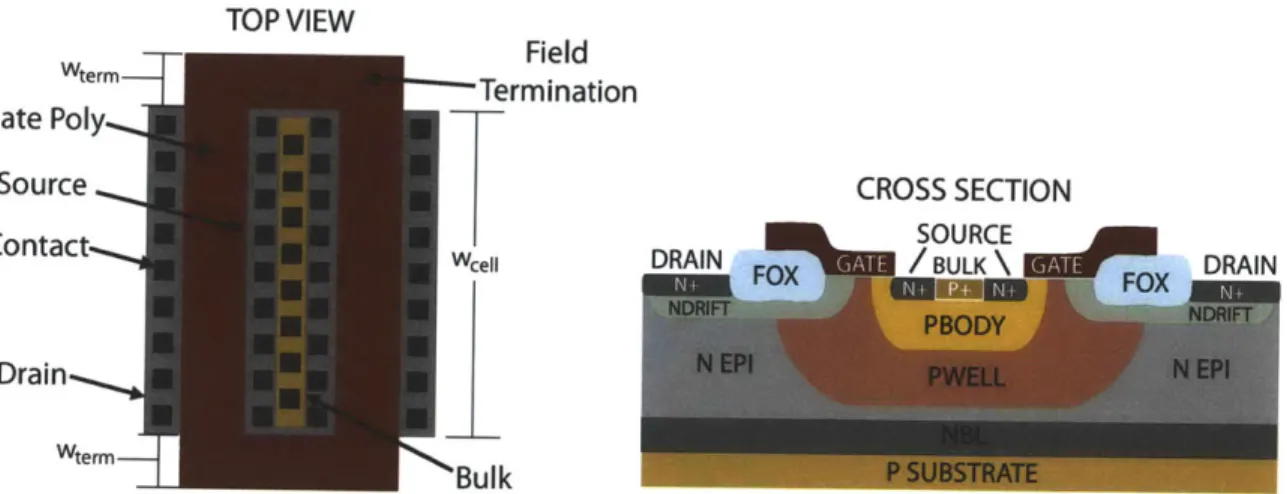
2.6 The top view of a single LDMOS cell. All the dimensions are fixed excepting
wcell which is scalable. . . . . 48
2.7 Layout overview showing the interconnect stack-up. . . . . 49
2.8 Each LDMOS cell comprises a ring of polysilicon, where two field termina-tions contribute capacitance but no additional conductance (depicted by the vertical gray bars in this illustration). As a result, increasing the number of cells to achieve a desired conductance will increase capacitance because the terminations take up more of the total device area. On the other hand, the gate resistance falls as the number of cells increases because of shorter poly runs and more gate contact points. This leads to an optimum Wcel .. . . . . 51
2.9 At a given device width, the aspect ratio has a strong effect on the overall performance. As the cells are stacked from a tall, narrow structure to a short, broad one, the gate resistance increases and the drain-source resistance decreases. In addition, Coss will rise because of the greater number of exposed junction ends. . . . . 52
2.10 The top layer of interconnect, metal-3 in this case, is chopped into a zipper-like structure. Each tooth experiences rising current from tip to base as successive rows are aggregated. In order to minimize the loss, the teeth are tapered to keep the current density more constant. The final taper angle is influenced by metal-2, via density, and relationship between the taper angle and final tooth count. ... ... 53
2.11 By breaking the device into a number of smaller devices separated by gate pad arrays, the total gate resistance can be dropped dramatically without strongly impacting RDS-on or device capacitance. . . . . 54
2.12 This network is used to calculate an equivalent gate resistance. The values are populated by relating the geometry and material constants in the device. Several similar networks are used to calculate interconnect resistance for the drain and source networks, as well. . . . . 56
2.13 Device power dissipation vs. cell width and aspect ratio for a 73.5 um device in the case-study converter example. . . . . 58
2.14 RDS-on vs. cell width and aspect ratio . . . . 58
2.15 Rgate vs. cell width and aspect ratio . . . . 58
2.16 F device layout . . . . 61
2.17 HV1 device layout with multiple-gate pad arrays and longer fingers . . . . 61
2.18 HV2 device layout with a square aspect possible for the introduction of copper top m etal . . . . 61
2.19 Switching trajectory for Class-<b2 Boost converter and an ideal hard-switched boost for the same voltage and power level. . . . . 63
List of Figures
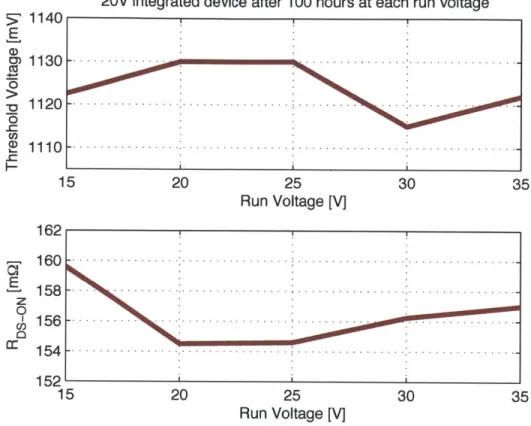
2.20 The shifts in VTH and RDS-ON are well within the established testing criteria. 65 2.21 After 1000 hours of operation at 35V, the 20V MV1 device has a total VTH
shift of around 20mV, and about a 4% change in RDS-ON. The allowable maximums are 1O0mV and 10%, respectively. . . . . 66
2.22 A Class-<D2 boost converter built using the MV1 device and operated to 35V.
It achieves 88% conversion efficiency at 17W, VIN=12V, VOUT=33V. . . . . 67 3.1 An isolated <b2 converter schematic including the transformer magnetizing
and leakage inductances. . . . . 71 3.2 A 4-layer transformer with a 1-turn primary and 3-turn secondary. Each
turn is on a separate layer which avoids increased loss due to flux shielding as compared to spiral designs. . . . . 72 3.3 Flowchart depicting general approach used to for synthesis . . . . 74 3.4 Concentric planar ring structure that [1] solves for mutual inductance. . . . 76 3.5 PCB geometry of a 2-winding spiral transformer. The parameters optimized
for are the diameter, d, the trace width, t,, the gap width, gw, and the z-spacing, z and the number of turns in each winding. . . . . 82
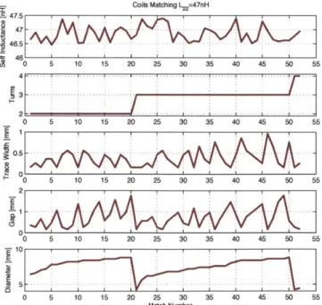
3.6 25 coils have the desired self inductance, L11. Their geometric parameters
are plotted together with the calculated inductance. . . . . 84
3.7 52 coils have the desired self inductance, L22. Their geometric parameters are plotted together with the calculated inductance. . . . . 84
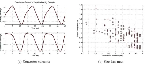
3.8 Plot of the successful transformer designs as captured analytically. ... 85 3.9 Converter currents used to baseline transformer performance and size-loss
map of successful transformer designs for isolated <b2 converter. . . . . 86 3.10 FastHenry transformer geometries from the 6.6 mm column arranged from
lowest efficiency to highest efficiency. More copper is favored in the primary winding owing to the higher currents. . . . . 87 3.11 Plot of the successful transformer designs as captured analytically. . . . . . 88 3.12 Fabricated PCB and measured results showing the discrepancy between
mea-surement and simulation as the transformer winding area becomes increas-ingly filled with copper. . . . .. . . . . 89 3.13 Comparison of analytical and simulated results for helical winding transformers. 91
3.14 The efficiency-diameter map for the helical winding series showing the perfor-mance of the various winding configurations. The best overall results come from the 1T-3T curve, which bounds the upper efficiency limit. . . . . 93
3.15 The efficiency-diameter map for the complete helical winding series allowing
independent scaling of turn dimensions as well as coil interleaving. . . . . . 96 3.16 Fabricated PCB and measured results for the helical winding transformers. 97 3.17 COMSOL simulation of a measured transformer geometry showing the
mag-netic field lines and current density in the coil cross sections when the sec-ondary is driven in sinusoidal steady state at 75 MHz. . . . . 99 3.18 Flowchart showing algorithm including radius compensation . . . . 100 3.19 PCB measurements vs. COMSOL simulation for helical transformers . . . . 101 3.20 Transformer #48 layout details . . . . 102
3.21 COMSOL simulation of the transformer secondary winding between two
plates shows that for a 1/2 radius spacing loss is barely affected and the change in inductance is small enough to be compensated by redesign. . . . . 102
3.22 Thermal measurement of the transformer in operation at 94% efficiency in
an Isolated 4D2 Converter . . . . 103
4.1 (D2 converters that exploit resonant networks and separation of energy storage
and control to achieve high efficiency at 10s of volts and 10s of MHz . . . . 106
4.2 A capacitively isolated )2 topology . . . . 107
4.3 A two winding transformer model with magnetizing and leakage inductances. 108 4.4 Transformation from 42 boost converter to isolated O2 converter . . . . 110
4.5 Volume comparison for a single transformer that meets the inductance pa-rameters and two transformer-inductor pairs that do the same at comparable efficiency. Case B uses a discrete solenoidal inductor that has roughly 4x the volume for the same board area as the planar components. The toroidal in-ductor in Case C, provided by George Hwang, is planar in the PCB. Case A is smaller volume-wise by about a factor of 3 over Case B, and 1.5 over Case
C . . . . .111
4.6 The resonant rectifier pictured is used for tuning purposes. The actual rec-tifier inductances are part of the transformer structure. . . . . 112 4.7 Power is controlled by adding a reactance in series with the resonant rectifier.
In order to calculate the desired value, the inverter is approximated as a sine wave with voltage equal to 4VIN/7r. The resistor RL1 is the describing function resistance of the rectifier derived from simulation . . . .... . . . 112 4.8 Tuning the rectifier to have a purely resistive input impedance at the
fun-damental (15.3-W and 8-W designs) increases efficiency but dramatically curtails the input voltage range. The horizontal black line in the bottom plot is the peak allowed VDS of the inverter power device. . . . . 116
List of Figures
4.9 Retuning the converters to have a small inductance in series with the rectifier offers wide load range and substantial improvement in efficiency over the original converter (11.4-W case) design. The horizontal black line in the bottom plot is the peak allowable VDS of the inverter power device . . . . . 118
4.10 Simulated waveforms from the initial isolated <D2 converter prototype. The bottommost plot shows that the rectifier is tuned slightly inductive per the tuning discussion in the previous section. . . . 120 4.11 Experimental isolated <D2 converter and the measured drain waveforms. This
converter suffers from input-loop parasitic inductance and diode losses that diminish output power and efficiency to 4 W and 37%, respectively. . . . . 121 4.12 Experimental isolated <b2 converter. The red ring indicates the approximate
current path that leads to input loop parasitic inductance. . . . 121 4.13 Translating the isolated dc-dc converter into an equivalent inverter network
helps to illustrate the effect of input parasitic inductance on this topology.
LPAR effectively forms an impedance divider with the load network,
nega-tively impacting output power and efficiency. . . . . 122 4.14 Various potential solutions to mitigate the effect of the input-loop parasitic
inductance. ... ... 123
4.15 Large-signal diode model used for VHF simulations . . . 124 4.16 Diode case temperature vs. input power is characterized and used to generate
the expected diode temperature rise during converter operation. Actual mea-surement shows a very steep increase over model predictions for the pulsating current waveforms in the resonant rectifier. . . . . 125
4.17 Tuned test rectifier transient and impedance simulation and measurements. 128
4.18 Diode temperature rise under AC and DC drive conditions. . . . . 129
4.19 As AC drive is increased, the peak forward voltage drop rises as well, dra-matically increasing diode loss. VREC is the voltage labeled in Figure 2.17b,
effectively the diode forward drop plus 12 V. . . . . 130
4.20 Schematic of diode test setup . . . 130 4.21 Performance of various diodes as power is modulated and rectifier
configura-tion is changed . . . 131 4.22 Final rectifier design versus original simulation. . . . 131 4.23 The converter impedance was simulated in SPICE and then measured
exper-imentally to ensure proper tuning. Iteration allowed for very close agreement. 132 4.24 Power was injected to each major loss component successively and used to
build a thermal model of the system. The linear behavior is evident from the plot and the successful curve fits to a linear model. . . . . 134
4.25 Results of thermal modeling show good agreement with SPICE and reveal the loss distribution in the converter. Data was obtained by repeated thermal im aging . . . . 135
4.26 Efficiency and power measurements of the final isolated prototype imple-mented with discrete MOSFETs . . . . 136
4.27 Converter waveforms for VIN=12V. Red curve is VDS, gray curve is VGS. - 136 5.1 Isolated <2 converter with 28-lead ETSSOP. The package footprint is more
than 10x the die area . . . . 137 5.2 Isolated <b2 converter architecture showing the relationship between the
con-verter IC and power stage components . . . . 139 5.3 Overview of the voltage-mode hysteretic control implemented with the IC. . 140 5.4 Converter IC and associated layout files. The IC is a 30-ball 6x5 array at
500 um pitch intended for flip-chip-on-board assembly. . . . . 141
5.5 Block diagram of the isolated 42 converter IC . . . . 142
5.6 Schematic of the half-sine resonant gate driver implemented on the IC . . . 142
5.7 Half-Sine resonant gate driver waveforms when no parasitic inductance is
included in the drain-source loop of the pull-down device. . . . . 146
5.8 Half-Sine resonant gate driver waveforms including parasitic inductance in
the drain-source loop of the pull-down device. . . . . 147
5.9 When the gate driver is started from a zero-state condition without
compen-sating for the lack of negative inductor current at to_, the first gate pulse is oversized, risking damage to the power device gate oxide. . . . . 149
5.10 By only charging the inductor during the first cycle after startup for half the
steady-state charging period, an over-voltage condition is avoided. . . . . . 150 5.11 The synchronizer and delay block . . . . 151 5.12 These are the simulated waveforms of the power stage, gate driver and
gate-driver control signals during a few modulation cycles . . . . 152 5.13 Schematic of the IV reference implemented on the chip . . . . 153
5.14 Opamp used in the IV reference with a boot-strapped biasing scheme that simplifies the design and makes startup of the IV reference easier. . . . . 155 5.15 Top-level schematic of the VLRO, which is used to generate a
temperature-stable clock waveform . . . . 155 5.16 The 9-stage ring oscillator comprising current starved inverters. It forms the
VCO used in the VLRO and has a minimum idle frequency of approximately 35 MHz to avoid startup problems. . . . . 156
List of Figures
5.17 Frequency-to-Voltage Converter used in the VLRO. It charges C6 with a constant current for a time equal to the low swing of CLK. This result is an output voltage proportional to frequency which is then fed back for regulation. 157
5.18 Opamp for the VLRO. . . . . 158 5.19 Wavforms for the VLRO from a cold start through lock. The system is in
lock when vfb equals vref. . . . . 160 5.20 The one-shot is a simple pulse generator comprising current-starved inverters
that are controlled to vary the pulse width. It is triggered on the positive state change of CLK . . . . 161 5.21 Regenerative comparator scheme used in the converter . . . . 162 5.22 Regenerative comparator scheme with adjustable hysteresis used to
imple-ment control of the converter. . . . . 164
5.23 Combined 5-V and 7-V linear regulators provide logic and auxiliary analog
supply rails. . . . . 165
5.24 The isolated communications system was kept as simple as possible and relies on capacitive isolation. The capacitors are realized as copper features in the PCB substrate. . . . . 166 5.25 A photograph of the Isolated (D2 converter shows that the inverter is quite
small without IC packaging to deal with. The rectifier is still relatively large because of diode packages. . . . 167
5.26 The non-isolated 4D2 boost converter with planar toroidal inductors printed in the PCB and associated schematic. . . . . 168 5.27 The IC mounted on the evaluation PCB used for bringup . . . 169 5.28 Gate drive waveform for properly tuned operation. . . . 171 5.29 Output power and open-loop efficiency for the isolated I2 converter
proto-type built using the custom IC . . . 172
5.30 Experimental gate and drain voltage waveforms for the isolated 42 converter
while operating under full load (6 W). . . . 172
5.31 (D2 boost converter power and efficiency measurements show the performance
to be higher in both aspects owing to the presence of a DC path that reduces resonating currents for a given output power. . . . . 173 5.32 The isolated 42 converter under closed loop modulation above 500 kHz. The
resulting output ripple is shown at the right, and is about 0.4% of the 12.7 V output. ... ... 174
5.33 Efficiency map of the isolated 42 converter vs. load under closed loop control for various input voltages . . . . 174
5.34 A comparison of the power density of various comparable isolated converters
with the isolated 'D2 converter presented in this work. . . . . 175
A.1 Isolated <D2 converter board - top copper layer . . . . 313
A.2 Isolated <D2 converter board - layer-2 copper . . . . 314
A.3 Isolated <D2 converter board - layer-3 copper . . . . 314
A.4 Isolated <D2 converter board - bottom copper layer . . . . 315
A.5 Isolated <D2 converter board - schematic . . . . 316
A.6 <b2 boost converter board - top copper layer . . . . 317
A.7 <D2 boost converter board - layer-2 copper . . . . 317
A.8 <D2 boost converter board - layer-3 copper . . . . 318
A.9 <D2 boost converter board - bottom copper layer . . . . 318
List of Tables
2.1 2.2 2.3 2.4 2.5 2.6 3.1 3.2 3.3 3.4 3.5 3.6VHF vs. Hard-Switched Loss Mechanisms . . . . 40
Measured Device Parameters . . . . 42
Optimization Parameters . . . . 51
Measured Device Parameters . . . . 59
Calculated Loss Comparison... . . . . . . . . . 60
Experimental DC-DC Converter Specifications . . . . 68
Spiral Coil Parameters . . . . 82
4-Layer Transformer Winding Configurations . . . . 93
4-Layer PCB Stack-Ups . . . . 95
Simulator Accuracy Comparison for 1T-3T transformer . . . . 98
Transformer #48 geometric parameters . . . . 100
Transformer #48 electrical parameters . . . 100
4.1 Component Values for Example Isolated Converter Designs . . . . 114
4.2 Simulated Loss Breakdown and Converter Efficiency for Isolated Converters 115 4.3 Component Values for Designs with Series Reactance . . . . 117
4.4 Component Values and Specifications for First Prototype Isolated (2 Converter 119 4.5 Diodes and Configurations Evaluated for Thermal Performance . . . . 128
4.6 Component Values and Specifications for Second Prototype Isolated #2 Con-verter ... ... 133
5.1 Targeted Converter Specifications . . . 139
5.2 IC Pin Descriptions . . . . 143
5.3 Register Bits and Description . . . . 166
5.4 Measured Converter Parameters . . . . 168
Chapter 1
Introduction
M
INIATURIZATION is the pursuit of modern technology. Today's smartphone packs a computing wallop that would have been considered magical' in the days of the Apollo program. Yet the consumer expects still more and so goes a silicon arms race, rushing ever closer to that elusive limit of semiconductor physics. Expectations aside, delivering on the promise our potent portables portend-the society-shaping fusion of information and person-is no small technical feat. As minimum feature size drifts south of 20 nm more functionality is squeezed onto less silicon, igniting an appetite for more power at steadily increasing density. While clever circuit, device, and systems solutions strive to quench this thirst, the desire for increased functionality and the availability of more energy-dense batteries ensure that power consumption in portables continues to rise. The result is continual increase in the demands made upon the power subsystem.
Taken in the context of increasing integration, the power management subsystem now oc-cupies a conspicuous area that could be otherwise spent on more functionality (several hun-dreds of millions of CMOS transistors, for instance), or smaller overall size. This is owing to the need for more power and the not-insignificant challenges that exist around shrinking the converter's energy storage. The latter is a thorny problem, and currently defines the limits on reduction of size, weight, and cost across the spectrum of power conversion. One means of reducing the size of the energy storage is is to increase switching frequency [2]. This allows for passive components to shrink as the amount of energy storage required to service the converter function falls. A small increase in frequency is generally not effective. For instance, in order to manage loss in magnetics as frequency is increased it's often necessary to decrease flux density yielding a counter-intuitive increase in passive component volume. Instead, operating in the VHF regime (30 MHz-300 MHz) offers the potential to utilize air-core inductors or low-permiability RF magnetic materials to achieve an overall size reduction while maintaining or improving performance in other areas such as efficiency, bandwidth, and power density. VHF power conversion has been demonstrated for voltage and power levels ranging from about a watt and a volt to hundreds of watts and hundreds
of volts. [3-8].
The approach to VHF power outlined in [3] has shown promise in discrete implimentations. However, while this has resulted in higher power density in many cases, significant reduction is still possible by going from discrete components to more integrated designs. This requires efforts on the fronts of power device development, passive components, circuits, and systems to be considered in concert. Exploration in these areas are the core of the thesis work presented here. Since a silicon power process that also provides CMOS is a prerequisite to integration, optimization of LDMOS (Lateral Double-Diffused MOSFETS) power devices was undertaken first. Once viable integrated power switches were demonstrated, work on passive components and circuit design was accomplished, ultimately leading to an attempt to increase converter density by using an IC designed for VHF converter operation in concert with a PCB substrate carrying a mix of embedded and surface-mount passives. The results are shown to be effective, if one overlooks an error in the IC design phase that led to an inability to demonstrate closed-loop operation without some external hardware.
In order to better frame the work presented here, the following two sections introduce a discussion of the loss mechanisms in hard switched power converters alongside the applica-tion of resonant techniques used to mitigate them. These consideraapplica-tions lie at the core of the VHF approach, but delivering on the promise of VHF to reach Lilliputian dimensions requires addressing the topics at the core of this work.
1.1
Losses in hard switched converters
A switched mode power converter constructed of ideal elements has no intrinsic loss
mech-anism. Rather, they arise inevitably from the use of real components. These losses, dis-tributed among the active and passive components constrain not only the efficiency of the
SMPS (switched mode power supply), but the size, cost, form-factor, and even converter
responsiveness. Finding ways to beat these losses is, in a sense, tantamount to miniaturiza-tion.
On considering a typical dc-dc converter, one fact that becomes obvious is that the bulk of the system, that is its weight and volume, comprises the passive energy storage elements. Semiconductor devices, having benefited from tremendous improvement since their incep-tion, occupy only a small fraction of a typical converter footprint. This is made clear in fig-ure 1.1 showing a common implementation of a synchronous buck converter where switches, gate drives, controller, startup and protection circuits, and the housekeeping power systems are integrated onto a die and placed in a QFN (quad flat-pack, no-lead) package. The remainder of the components are the energy storage devices which require roughly an addi-tional four times the board area (not accounting for interconnect) and nearly six times the
1.1 Losses in hard switched converters
T 2.T
Figure 1.1: Synchronous buck converter active vs. passive volume. The synchronous buck converter components pictured will supply 7.5 W into 5 V. The QFN on the left encompasses the active switches, gate drive, control, and housekeeping functions. The remaining passive elements require 4 times the board area and 6 times the volume, not accounting for board interconnect.
volume. It is not surprising, then, that techniques to reduce converter footprint might be aimed at minimizing or eliminating passive energy storage.
Where the goal is to reduce the size of the energy storage components, there are two primary ways to proceed. Either energy density may be increased or total converter energy storage reduced. Increasing the energy density implies shrinking a device for a constant amount of storage. Even if this can be accomplished, given the physical constraints imposed by power dissipation, the increased losses that result often cannot be reconciled with good converter performance. Considering a solenoidal inductor, it is demonstrated in [9] that fundamen-tal scaling between linear dimensions and flux- or current-carrying area causes inductor
Q
to decrease as a2 where a < 1 is a constant scaling each linear dimension. Similar rela-tionships are enumerated in [10] for other geometries. In the case of capacitors, analogous problems arise. Where a given dielectric material is available, a lower bound exists on the capacitor plate separation for a set working voltage. Further, plate resistance also increases as plate thickness is decreased or plate area is increased, both are necessary to improve energy density. These conditions imply that the capacitor
Q
will become unacceptably low with continued scaling at a constant capacitance. Thus a host of factors -Q,
dielectric breakdown, and dissipation - impose a maximum energy density on passive components. Unfortunately, practical densities leave something to be desired for converter size.With very limited leeway to increase energy density, we turn our attention to reducing the required energy storage. The classic solution is to raise the switching frequency [2], thereby reducing the amount of energy processed per cycle, a condition that leads directly to smaller numerical values of inductance and capacitance. The flyback converter in figure 1.2 is a convenient means to an explanation.
VIN
+
q IO
LF
%_ORL(a) Buck-boost converter
M1 'CH
MOUT IDCH D
VIN + qNt) LF
COUT
RL VIN OURLT
'DCH
YCd
H
A
L
LD
ILD
(b) First part of cycle (c) Second part of cycle
Figure 1.2: Buck-Boost Converter Illustrating Energy Storage Requirements. In the buck-boost converter, LF acts as temporary storage. In the first part of the cycle LF is charged
by current ICH while COUT holds up the output. In the second portion of the cycle LF discharges into the load while replenishing COUT.
The buck-boost converter is an indirect converter. This type of converter transfers energy from the source to intermediate storage in the first portion of a cycle and then from inter-mediate storage to the load in the second portion of the cycle. The interinter-mediate storage in the flyback converter is the inductor, LF. As the switching frequency is increased and the amount of energy processed each cycle gets smaller, the numerical value LF can be reduced and the inductor made physically smaller for constant energy density. The same applies to the capacitors CIN and COUT. For instance, COUT must hold up the output voltage during the half of the cycle when LF is charging. The holdup time is inversely proportional to frequency as is the associated RC time constant for a constant droop in output voltage. Another way to see that COUT can be reduced is to consider that RL and COUT form a low-pass filter which attenuates the switching ripple. As the switching frequency increases the low-pass corner frequency moves up for a given attenuation, relaxing the capacitance requirement.
Though increased switching frequency attends less energy storage, it is not a technique that may be used haphazardly: A cohort of loss mechanisms arise rapidly to place limits on
1.1 Losses in hard switched converters
the operating frequency. While not necessarily the largest of these, important frequency dependent losses in passive elements are limited almost exclusively to inductors and their magnetic materials. Most magnetic materials, used to increase inductance per unit volume, operate well at low frequency but have losses that rise rapidly otherwise. The basic trend is captured by the Steinmetz equation:
Pv(t) = kfaBR (1.1)
where P (t) is the time-average loss per unit volume [kW/m2], B is the peak ac flux am-plitude [Gauss],
f
is the frequency of sinusoidal excitation [Hz], and the constants k, a,and
#
are found by curve fitting. Examining 1.1 it is clear that for a greater than one (it's often in the range of 1-3) that the loss will rise briskly with frequency. Another important implication is that the core volume may be increased to reduce the flux density, trading increased size for higher frequency-the opposite of the desired effect2. In truth, theStein-metz equation is only valid in a narrow range of situations, primarily where the excitation is sinusoidal and relatively low frequency. At high frequencies and under the non-sinusoidal excitation typical of power converters, the losses tend to be greater than predicted in the Steinmetz model and many different modeling approaches have been undertaken to get a more accurate prediction (for instance, [11]). The upshot, however, is that most bulk magnetic materials are not suitable for operation at frequencies much higher than a few megahertz.
One way of avoiding magnetic core losses is to do away with the magnetic core. The lower energy density demands even higher operating frequencies, but to the extent that the frequency can be increased, the magnetic loss picture looks much better. For a simple air core inductor, the inductance and resistance are determined primarily by geometry and the choice of conductor. Inductor quality factor
Q
is:wL
Q
= (1.2)R
In this simple relationship, expressing the ratio of energy stored to energy lost per cycle,
Q
increases with reactance and decreases with resistance. The frequency dependence of R and L are very difficult to calculate for any geometry other than isolated straight wires. In general, skin effect, proximity effect, and interwinding capacitance affect both L and R [10].If the proximity effect and the interwinding capacitance are ignored, the skin effect results
2
Often loss becomes the limiting factor at high frequency and flux derating is necessary to avoid excessive heat build up. Thus at high frequency cored inductors can actually get larger.
D CGD LD RDS
G
RG DB DCDS CGS LsS
Figure 1.3: A MOSFET model including parasitic elements usually important in hard switched dc-dc converter design
in approximately a square-root increase in resistance with frequency. Since reactance rises linearly under these assumptions, then
Q
will increase oc Vf. Measurements of inductorQ
and information available from manufacturers of air-core RF inductors indeed show thatQ
increases with frequency as a general trend.The seemingly synergistic effect of increasing
Q
with frequency for air-core inductors is only advantageous provided that the other frequency dependent loss factors are dealt with. These losses are associated with active semiconductor devices. Semiconductor losses can be divided into three main mechanisms for MOSFETs: conduction loss, switching loss, and gating loss. A MOSFET model including the parasitic elements usually considered in dc-dc converter design is shown in fig. 1.3.Conduction loss, due to the effective resistance of the channel, the lightly doped drain region (LDD), and metal/bondwire resistance, is only slightly frequency dependent3. Switching
loss, however, depends significantly on frequency. It is helpful to further divide switching
loss into overlap loss and losses resulting from discharge of the drain-source capacitance,
CDS. Overlap loss refers to the condition where the MOSFET supports simultaneous voltage and current at its drain-source port and thereby dissipates power. This condition arises from the need to charge or discharge the device channel through finite source impedance (whether this impedance arises externally or as a result of device parasitic resistance and inductance) which imposes a minimum on switch transition times. Simplified models of overlap loss
3
At typical operating frequencies the quasistatic assumptions for MOSFETs are valid, so the channel and
LDD components of RDS-ON are constant. Bondwire resistance is usually a small enough component that skin effect only accounts for a small change in the total RDS-ON.
1.1 Losses in hard switched converters
parameterized in converter nominal voltage (Vo) and current (Io), and MOSFET rise (Tr) and fall (rf) times are readily available [2, 12]:
Er + Ef = kVoIO(Tr + Tf) (1.3)
The constant k reflects the circuit in which the device is used and varies between 1/6 and 1/2 depending on whether the load is purely resistive or clamped inductive. Since this result is basically fixed once the device and circuit are chosen, the energy per transition (Er
+
Ef)is also fixed. Therefore, as switching frequency rises, so does overlap loss.
The loss due to CDS occurs at device turn on, when the energy stored on the output capacitance is dumped into the switch yielding a loss than can be roughly approximated
as:
}CDSvGATE-PKf.
This effect can be significant even at frequencies well below amegahertz-CDs is usually fully charged just before turn-off.
Gating loss results from charging and discharging the input capacitance, CISS = CGS +
CGD. Calculating the gating loss is somewhat complicated by the presence of CGD which is multiplied according to the Miller effect during transitions. In lateral MOSFETs where
CGD tends to be very small and its effects can be ignored, the gating loss is approximately expressed as:
PGATE = CGS vGATE-PKf
(1.4)
This reflects that the loss is associated with the loss of charging a capacitor from a dc
voltage through a resistor, ICY2, and the subsequent dumping of the stored energy once
per cycle. In other types of MOSFETs, such as vertical DMOS and even some lateral devices,
CGD is a significant portion of CISS and the effects can't be ignored. Then the gate power
is usually expressed in terms of the total charge required per cycle to enhance the device:
PGATE = QGVGATEPKf (1.5)
In both cases the frequency dependence is clearly linear. This mechanism becomes impor-tant at switching frequencies of a few megahertz and beyond where gating loss for typical devices can range from hundreds of milliwatts to several watts.
Diodes also account for a fraction of the converter loss budget. All diodes have an associated forward voltage drop, VF, that combines with the forward current, IF, and resistive losses in the bulk regions to result in diode conduction loss. This mechanism is not explicitly frequency dependent. PN-junction diodes and PIN diodes, however, do have a frequency dependent loss mechanism - reverse recovery. Reverse recovery names the process in which stored minority carriers are removed during commutation. During the reverse recovery time, TRR, the carriers are extracted across a constant voltage. Since this time is related to the amount of stored charge and the impedance of the external circuit, TRR is fixed for a given configuration. Therefore, the energy wasted per cycle to reverse recovery is constant implying frequency dependence. Schottky diodes, which are formed as metal-semiconductor junctions are majority carrier devices. They do not suffer heavily from reverse recovery losses, but are only available with breakdown voltages below about 120 volts.
1.2
Resonant Power Conversion
Resonance, usually ascribed to systems with complex poles displaying oscillatory behavior, is of some significance in power conversion. In filtering, for example, it plays a role to develop large immitance in comparatively little volume4. Here we look at resonance as a means to push back converter loss mechanisms and realize operation in the very high frequency regime (VHF, 30 MHz - 300 MHz).
A number of converter topologies exist that draw from RF amplifier techniques to achieve
efficient energy conversion [5, 14-21] at high frequencies. These designs rely on reactive networks to shape the switch voltage and current and reduce switching loss. The class E converter, fig. 1.4a, is a widely practiced topology whose network enforces a zero-voltage switching (ZVS) opportunity at turn-on. Its basic operation can be classified as indirect. The inductor LCHOKE is an open at the switching frequency, ensuring that only dc current flows from the source. With no dc path to the load energy from the source must first be stored on the switch shunt capacitor Cp. The energy stored in Cp then rings towards the load in a cycle that is determined by the switching function, q(t), and the resonant tank
formed by the load, LRES, and CRES. It functions by ringing the energy on CDS to the load
once per cycle. When these components are tuned according to [14,15], the drain voltage will naturally return to zero as the energy in Cp rings toward the load. At this point, the switch may be turned on with minimal loss. This mode of operation avoids the losses
4
Series and parallel resonant filters can be used to shunt or block ripple in power converters. It was demonstrated in [13] that by using resonance, filter element volume could be reduced by better than a factor of three.
1.2 Resonant Power Conversion
usually ascribed to the switch drain-source capacitance and largely avoids overlap loss, as well.
In practice, the drawbacks of such resonant topologies have prevented them from seeing widespread use. To begin with, the load range is severely restricted when compared with the 100:1 or better range achievable with conventional converters. Resonating losses from circulating reactive currents become significant as the load is reduced, hurting efficiency.
-CHOKE LRES CRES
VIN M1 ,R
CP
RL._q(t)d
(a) Class E inverter
Effect of Load Change on Class-E Converter Waveforms and Efficiency
640 0 5 10 15 20 25 30 35 Time [ns] 510 80 - - - -7 0 --. -.-.-.-.--.-.--.. .. 2 3 4 5 6 7 8 9 10 Load Resistance [Q]
(b) 50 MHz Class E drain voltage waveforms
Figure 1.4: Resonant topologies often suffer from limited load range in power conversion applications. Here, the Class E inverter waveforms are pictured as the load is varied from Rto 2R. The properly tuned waveform is displayed in heavy black. The loss of ZVS and negative impact on efficiency are evident.
VREF comp drive eI dc-dcd I c
converter CBULK RL
Figure 1.5: Schematic depiction of VHF converter under on-off modulation. The closed-loop system keeps output voltage constant allowing the converter to deliver a constant power (effectively it sees a constant load) at it's most efficient point. Actual power delivered to the load depends on the duty ratio of the control signal.
The situation is made worse in the many cases where the load is an integral part of the res-onance. Then, any change in load disrupts the ZVS condition and switching loss inevitably arises. This situation is depicted in fig. 1.4b. Further difficulty arises because duty ratio control is often not possible. Instead, control is achieved by varying the switching frequency. The resulting poor dynamics worsen with frequency and place an artificial upper bound on practically achievable switching speed. Many resonant converters also suffer from high peak switch stresses. The class E converter, in particular, has peak drain voltages rising as high as 4.4 times the dc input voltage [22]. This is particularly troublesome where integration is concerned because integrated devices tend to have lower breakdown voltages.
Several of these issues can be resolved by partitioning the energy storage and control func-tions [3,4,23]. Instead of controlling the output by varying the switching frequency, on-off modulation of the converter determines the fraction of output power delivered (see fig. 1.5). When the converter is on, it delivers a fixed power maintaining ZVS and maximum effi-ciency. When off, no power is delivered and there are no associated resonating losses. Under these conditions, the load range is a function of the minimum achievable modulation index. Such operation allows the network to be tuned to enforce ZVS at one particular operating point. The result is maximum efficiency, better dynamics, and higher achievable operating frequency. The fact that this mode of operation allows much higher switching frequency is self-reinforcing-high frequency means less energy storage so the converter can be started and stopped more rapidly and achieve a wider load range.
1.3 Contributions and Organization of the Thesis
1.3
Contributions and Organization of the Thesis
Raising the switching frequency is a well known means of reducing required storage in power converters. It is precisely this reduction that can put inductor and capacitor values into the range that they might be considered for integration. For inductors, in particular, VHF operation allows magnetic materials to be set aside, avoiding the difficulty and expense of incorporating them on chip or on board. Capacitors benefit from similar consideration primarily owing to the much smaller required values. However, simply moving to higher frequency is not enough. Existing power devices that satisfy VHF operation tend to be RF LDMOSFETs which are usually over-packaged, optimized for linearity versus more desireable characteristics for power transfer, usually only come in a few discrete ranges, and are difficult to drive owing to gate-loop parasitic inductance as well as drain feedback via
CRSS. In addition, control, driver, and hotel circuits implemented with discrete components become a significant portion of converter size after power-stage passives are shrunken via increased switching frequency. When these facts are considered jointly, it is clear that integrated LDMOS would be of great benefit, since the control and power devices can be absorbed onto the same die. The prerequisite here is that the power devices be "good enough." In conjunction with an on die methodology for the semiconductors, furthering the goal of being small and cheap includes addressing passive design issues that permit batch fabrication and lower component counts. Finally, overall system design needs consideration to achieve the best tradeoffs for size and performance. The ensuing chapters address the topics in turn.
Chapter 2 examines methods to improve integrated LDMOS performance for use in VHF applications. Most LDMOS available in integrated form have been optimized primarily for the hard-switched application. This has implications both in terms of the differing loss mechanisms between the hard-switched and VHF soft-switched operating modes and the safe operating area (SOA). The chapter first examines the loss mechanisms peculiar to soft-switched VHF operation, then presents a methodology for optimizing device layout in their consideration. The improvement in performance is substantial (over 50% loss reduction in the semiconductor) post-optimization. Further work is accomplished as regards the
SOA. Normally, SOA in an LDMOS is set by a combination of BvDss and hot-carrier
effects. With a switching trajectory that strays to simultaneous high voltage and current, the hard switched case tends to find its most severe constraints in the hot-carrier regime. In this chapter we look at relaxing SOA requirements based on a soft-switching trajectory and provide reasonable evidence that working voltages much closer to Bvss may be used with converters like the <D2. As a result, devices with lower per-unit capacitance yield higher performance. Simultaneous optimization of layout and relaxation of the SOA yield
a greater than 70% reduction in device loss showing integrated LDMOS to be feasible for VHF operation.
The networks that are utilized to achieve VHF operation come with the caveats of tuning and component count. The latter not only makes the converter more difficult to shrink (since more power-stage interconnect is necessary), but also harder to tune. Chapter 3 looks at a means to reduce component count and provide repeatability for the passives in the resonant power stage. Specifically, a technique for synthesizing a transformer that provides both galvanic isolation and the bulk of the magnetic energy storage is presented.
By absorbing some of the inductors into the transformer parasitics, the component count
is reduced. Printing the transformer on a PCB helps to mitigate variability and achieve more consistent tuning. However, these requirements necessitate that the transformer have a fully-specified inductance matrix. Since a given inductance matrix can be realized by any number of physical transformer implementations, we examine how to synthesize devices that both meet the electrical requirements and have a good loss-volume tradeoff in this inverse-problem space.
Chapter 4 develops an isolated <D2 converter. This converter is both a platform to utilize the transformer designs of Chapter 3 and a demonstration of furthered circuit design tech-niques. A number of design tradeoffs in the circuit regime arise during the development of the isolated <D2 converter. These are addressed and their implications exposed. Challenges around diode performance and modeling at VHF also cropped up as part of the isolated <b2 converter design. This investigation and the results of diode performance studies are pre-sented. A thermal resistance model of the converter system is created and used to model the loss distribution in the converter. This allowed informed iteration to improve the over-all performance of the system as well as a degree of validation of the VHF loss modeling efforts undertaken to date. The combination of these efforts yields an isolated VHF power converter with good power density.
The goal of this work, miniaturization of power converters, is examined most directly in Chapter 5. An IC power process is chosen as the basis for a converter design. Optimization of the available power devices is followed by the design of a VHF gate driver that takes advantage of the integrated regime and demonstrates superior performance to thus-far im-plemented discrete designs. A number of challenges are overcome by taking advantage of on-die opportunities such as more precise timing and the relative absence of loop induc-tance among critical circuit components. This allows for a more-integrated version of the isolated <D2 converter of Chapter 4. Control and hotel components are pulled on die while magnetics are printed in the board and capacitors remain small surface-mount components.
1.3 Contributions and Organization of the Thesis
The concluding chapter summarizes the results of the work and looks forward to future potential.
Chapter 2
Power Device Optimization
2.1
VHF Device Loss Model
2.1.1
Overview
S
EMICONDUCTOR device losses place critical limits on the design and performance of power converters. As a result, significant effort has been devoted to the optimization of power devices. Most converters operate under hard-switching conditions, or at frequencies below a few megahertz, and optimization has focused on reducing loss under these condi-tions. This has led to devices that are very good for these applications, but do not realize the potential of power silicon in the VHF regime. In this work, optimization is accomplished for the set of device losses that result when soft switching is employed to attain very high switching frequencies. This requires a model that captures the loss mechanisms and their scaling behaviors such as the one proposed in Section 2.1.2.2.1.2
VHF Device Losses
To construct a model to optimize devices for VHF operation it is first necessary to consider the loss mechanisms of interest and their scaling behaviors. In general, to achieve extreme high frequency operation requires a means of rescaling or otherwise mitigating frequency-dependent loss. One example of a circuit topology that achieves this result is the Class-<b2
converter illustrated in Figure 2.1 [6]. It employs fully-resonant switching and soft-gating to enable efficient operation in the VHF regime. The application of these techniques render overlap loss and capacitive discharge losses at both the gate and drain ports insignif-icant. This permits scaling the switching frequency until a new set of frequency dependent losses obtains. These VHF losses derive from the recirculation of energy stored in the de-vice parasitics through lossy media, rather than its complete dissipation. As a result their scaling behaviors and values (normalized to converter output power) differ. These are the parameters that must be considered when optimizing devices for the VHF regime.


![Figure 3.4: Concentric planar ring structure that [1] solves for mutual inductance.](https://thumb-eu.123doks.com/thumbv2/123doknet/14687772.560549/76.918.249.682.161.571/figure-concentric-planar-ring-structure-solves-mutual-inductance.webp)