Design of a Silicon Carbide Micro-Hotplate Geometry
for High Temperature Chemical Sensing
Gregory Benn B.S. Aerospace Engineering University of Colorado, Boulder, 1999
Submitted to the Department of Aeronautics and Astronautics in partial fulfillment of the requirements for the degree of
MASTER OF SCIENCE IN AERONAUTICS AND
ASTRONAUTICS
at the
MASSACHUSETTS INSTITUTE OF TECHNOLOGY
May 2001©
2001 Gregory Benn. All Rights Reserved.The author hereby grants to MIT permission to reproduce and to distribute publicly paper and electronic copies of this thesis
docu-ment in whole or in part.
09
n 1
MASSACHUSETTS INSTITUTE OF TECHNOLOGYA UG
1 9 2002'TE
LIBRARIES
AERO
Author...
- . . ... ... . . . .ment of Aeronautics and Astronautics
August 15, 2000 Certified by Certified by Accepted by ... ..,r ... \ / ... John Brisson ssociate Professor, Department of Mechanical Engineering Thesis Supervisor
VOf
VMark SpearingEsher and Harold E. Edgerton Asssociate Professor, Department of Aeronautics and Astronautics Thesis Reader
...
Wallace E. Vander Velde Professor Emeritus, Department of Aeronautics and Astronautics Chairman, Committee of Graduate Studies
MASSACHUSETTS INSTITUTE OF TECHNOLOGY
LIBRARIES
Design of a Silicon Carbide Micro-Hotplate Geometry for High
Temperature Chemical Sensing
by Gregory Benn
Submitted to the Department of Aeronautics and Astronautics on May 25, 2001, in partial fulfillment of the requirements for the degree of Master of Engineering in Aeronautics and Astronautics
Abstract
Silicon carbide, high temperature, chemical sensors are the next step in chemical detection technology; allowing for the development of low cost, robust, lower power, and widely applicable chemical sensors. SiC offers the thermal conductivity, electrical properties, and operating temperatures not currently available in silicon sensors. Boston Micro Systems, a Wobum, Massachusetts based company, has developed technologies for bulk manufactur-ing of smanufactur-ingle crystal SiC material. Usmanufactur-ing this technology, geometries optimizmanufactur-ing thermal and electrical performance have been developed to create a SiC micro-hotplate for chemi-cal sensors.
Under etching allows for the manufacturing of micro-hotplates. Micro hotplates allow sensors to discriminate between chemical species by controlling absorption and desorp-tion of chemicals. Optimizadesorp-tion of the performance of such a device is achieved by devel-oping hotplates that are suspended by necked tethers. Tether designs minimize heat lose from the hotplate and necking creates heat generation regions. The excellent thermal prop-erties of SiC allow heat to be transferred from the necked tethers to the hotplate; produc-ing a hotplate with a uniform temperature distribution, important to the sensitivity and accuracy of the sensing film.
Testing of tethered and necked hotplates identified several areas of improvement in hot-plate design. These include under etching, improvement in the hot-plates response to thermal
stresses, and p-n junction performance improvements.
Using such design improvements as tethers and necking the thermal performance of SiC micro-hotplates has improved by two orders of magnitude. This thesis discusses the
design, modeling, and testing of single crystal SiC micro-hotplates. Advisor: John Brisson
Table of Contents
Table of Contents ... 5
L ist o f F ig u re s ... 7
L ist o f T ab le s ... 9
A cknow ledgm ents...11
List of A cronym s...13
S y m b o ls ... 1 5 1 . In tro d u ctio n ... 17
1. 1 Project Overview ... 17
1.2 Basic D evice Overview ... 18
1.3 Project Objectives ... 19 1.4 Thesis O verview ... 21 2. Background ... 23 2.1 Chapter Overview ... 23 2 .2 M a te ria l ... 2 3 2.3 P-n Junctions ... 24
2.4 Chem ical Sensing ... 25
2.5 Conclusions ... 28
3. Initial D esign Analysis...29
3.1 Chapter Overview ... 29
3.2 G eom etry ... 29
3.3 M odeling A ssum ptions ... 30
3.4 Perform ance Analysis of Original Design ... 32
3.5 Conclusions ... 35
4. First D esign Iteration...37
4.1 Chapter Overview ... 37
4.2 G eom etry ... 37
4.3 M odeling A ssum ptions ... 38
4.4 Perform ance A nalysis of First Iteration Design... 39
4.5 Conclusions ... 42
5. Second D esign Iteration ... 45
5.1 Chapter Overview ... 45
5.2 Geom etry of Long Tethered Plate ... 45
5.3 Modeling Assumptions and Calculations for Long Tethered Plate ... 47
5.4 Finite D ifference Results for Long Tethered D esign... 53
5.5 Finite Elem ent Results for Long Tethered Design... 55
5.6 Conclusions ... 55
6. Tether D esign and the Final Design... 57
6.1 Chapter Overview ... 57
6.2 Length Considerations... 57
6.3 Tether N ecking ... 60
6.4 Analysis of N ecked Tether Design... 67
6.5 D esign Com parisons ... 70
6.6 Conclusions ... 72
7. Tem perature D ependent Properties... 75
7.1 Chapter Overview ... 75
7.2 M easuring Electrical Properties Dependent on Tem perature ... 76
7.3 M odeling the Electrical Properties ... 80
7.4 Tem perature Dependence of Therm al Properties... 85
7.5 Conclusions ... 90
8. Device Testing ... 91
8.1 Chapter Overview ... 91
8.2 Experim ental Set-Up ... 91
8.3 Experim ent Results ... 96
8.4 Analysis of Experim ent ... 98
8.5 Conclusions ... 103
9 . C o n c lu sio n s ... 10 5 9.1 Design Overview ... 105
9 .2 L e sso n s ... 10 6 9.3 Future W ork ... 107
Appendix A Finite Differencing of the Hotplate. ... 109
A .1 Overview ... 109
A .2 Finite Differencing Technique ... 109
Appendix B Finite Elem ent Analysis and ADINA ... 115
B . O v erv iew ... 1 1 5 B.2 M athem atical M odel using FEM ... 115
B.3 Transient Response M odeling ... 120
B.4 ADINA m odeling ... 121
Appendix A Test Device M ask Sets ... 123
A . O v e rv iew ... 12 3 A .2 Tested designs ... 123
A .3 Non-Tested Designs ... 125
List of Figures
F ig u re 1.1: B a sic d e sig n ... 18
Figure 1.2: B asic design layouts ... 22
Figure 2.1: Structure of unetched w afer... 25
Figure 2.2: Programmed temperature response of a tin oxide micro-hotplate to a series of organic v ap o rs (fro m N IS T ) [1] ... 2 7 Figure 3.1: Initial plate design ... 30
Figure 3.2: Analytical temperature distribution over the initial plate design ... 34
Figure 3.3: Interior grid designations for finite difference method ... 35
Figure 3.4: Tem perature distribution over plate ... 36
Figure 4. 1: First design iteration (plate section only)...38
Figure 4.2: Temperature distribution over plate of first design iteration... 40
Figure 4.3: Temperature distribution over the plate center and plate edges respectively...40
Figure 4.4: Temperature distribution over 40 mm tether design ... 41
Figure 4.5: Center and end temperature distribtuion for 40 mm tethers...42
Figure 5.1: Long tether design layout ... 46
Figure 5.2: Fintie elem ent breakdow n ... 49
Figure 5.3: Finite difference results for long tether design... 54
Figure 5.4: Temperature distribution over the center (AA') and edge (BB') of the plate ... 54
Figure 5.5: Finite element results for 240 mm tether design ... 56
Figure 6.1: Temperature distribution over 240 mm tethers ... 59
Figure 6.2: N ecked tether design ... 60
Figure 6.3: N ecked tether layout... 61
Figure 6.4: Comparison of temperature distribution for different neck lengths at a constant current o f 0 .4 8 8 m A ... 6 3 Figure 6.5: Necking length vs current required at a constant plate temperature of 1000K ... 64
Figure 6.6: Necked length vs voltage at a constant plate temperature of 1000 K...65
Figure 6.7: Necked length vs power at a constant plate temperature of 1000 K ... 65
Figure 6.8: Comparison of temperature distributions of different necking lengths for a constant plate tem p eratu re o f 10 0 0 K ... 6 6 Figure 6.9: Comparison of heat transfer rate of different necking lengths at a constant plate temper-atu re o f 10 0 0 K ... 6 7 Figure 6.10: Temperature distribution of necked tether design ... 68
Figure 6.11: Drive voltage of four main designs at 1000 K... 71
Figure 6.12: Power comparison of four main designs at 1000 K...72
Figure 7.1: Four point probe test structure... 77
Figure 7.2: Results of Resistance vs Temperature Tests, Chip #1... 79
Figure 7.3: Results of Resistance vs Temperature Tests, Chip #2... 79
Figure 7.4: Plot of log(R/T3/2) vs 1/T and a linear curve fit to the non degraded data for chip #1 ... 83 Figure 7.5: Chip #1, comparison of experimental results to modeling fit ... 83
Figure 7.6: Chip #2, Comparison of Experimental Results to Modeling Fit ... 84
Figure 7.7: Temperature dependence of resistivity based on model results for chip #1...84
Figure 7.8: Research Results for Temperature Dependence of SiC for a 1018 cm-3 Doping Density 86 Figure 7.9: Test Structure to Measure Thermal Conductivity ... 87
Figure 7.10: Temperature Over the Bridge Structure ... 88
Figure 8. 1: Test plate layout...92
Figure 8.2: Circular TLM pattern...93
Figure 8.3: M anufactured hotplate ... 94
Figure 8.4: M icro-machined tethers... 94
Figure 8.5: Tether-hotplate junction ... 95
Figure 8.6: Tether hotplate junction and contact pad... 95
Figure 8.7: Basic modeling of experimental results... 99
Figure 8.8: M odel of final device results ... 100
Figure 8.9: Buckling model of tethers...101
Figure 8.10: Deflection modeling of tethers ... 102
Figure 8.11: Modeling tether bending to determine the vertical deflection of the tether ... 102
Figure A. 1: Nodal layout for finite difference method ... 110
Figure A.2: Edge element for finite difference method ... 112
Figure A.3: Inside corner element for finite difference method ... 112
Figure A.4: ... Outside corner for finite differencingl 13 Figure B.1: General finite element body...116
Figure B.2: Example finite element ... 119
Figure C.1: Test Device 1, Large Perforations ... 123
Figure C.2: Test Device 2, Small Perforations ... 124
Figure C.3: Test Device 3, Necking and Large Perforations ... 124
Figure C.4: Test Device 4, 64 mm Tethers, Large Perforations ... 125
Figure C.5: Test Device 5, 440 mm Tethers, 200 x 200 mm Plate ... 125
List of Tables
Table 2.1: SiC room tem perature properties [6,7,8]. ... 23 Table 8. 1: Comparison of expected verses measured resistances... 96 Table 8.2: A djusted resistance com parison... 97
Acknowledgments
As with most graduate students, this work reflects the efforts of many people, not just the person with their name on the cover. It is the culmination of work between professor and student, lab and company, husband and wife (to be), friends, and family. As such, there are several people who contributed to this work who I would like to thank with all my heart for there effort, support, and guidance.
First, to Professor John Brisson. Without his advice and guidance this project would have never even begun, and never finished.
Professor Mark Spearing who helped get me this project and provided insight into the mechanics of micro devices. An invaluable wealth of information related to micro struc-tures.
A special thanks to Rick Mlcak and Boston Micro Systems. First, for their funding of the project, but more importantly for their advice, their time and patience, and the use of their facilities. And a special thanks to Rick for all of his help and wisdom. I learned so much from him about semiconductors and micro machining I am forever indebted. I can only hope that this work helps to make a profitable and successful product for BMS.
To the love of my life and best friend, Cari. For her countless hours of editing and fax-ing of thesis drafts. For her tireless support, attentive ear, and comfortfax-ing voice. For allow-ing me to go 2000 miles away from her for two years to get this degree. I love you with all my heart.
To my parents and family, Mom and Dad, Sally, Brian, and Jeff. For always supporting me and believing in me, not just for this work, but everything in my life. This work is the
culmination of 24 years of life, of growing and learning.
List of Acronyms
BMS Boston Microsystems
MEMS Micro Electrical Mechanical System
SiC Silicon Carbide
FEM Finite Element Modeling TLM Transmission Line Method
ADINA Automatic Dynamic Incremental Nonlinear Analysis NIST National Institute for Standards and Tests
Symbols
B Temperature gradient interpolation gradientc Specific heat, J/kg-K
e Elementary charge, C
Ed Donor energy, J
H Element temperature interpolation matrix h Convective heat transfer coefficient, W/m2-K k Thermal conductivity, W/m-K k Boltzmann constant, J/K K Conductivity matrix Kc Convection matrix L Length, m P Power, W m* Effective mass, kg ND Doping density, cm-3
n Density of free electrons, cm-3 qdot Heat generation per unit volume
Q
Heat flow input, Wq Heat transfer rate, W q" Heat flux, W/m2
qB Internal heat generation, W/m-K qS Surface heat flow, W/m
2
R Resistance, Ohm
T Temperature, K
TS Surface temperature, K
Tinf Temperature of and infinite mass of surrounding air
t Thickness
V Volume, m
w Width, m
x Position, m
0 Virtual temperature distribution O Temperature distribution
0' Heat change with position, heat flow, W/m Mobility, cm2/V-s
p Resistivity, Ohm-cm, density, kg/m3 G Electrical conductivity, 1/Ohm-cm
a Thermal expansion coefficient, K~1
Chapter
1
Introduction
1.1 Project Overview
Micro-machined chemical sensing devices improve the functionality of chemical sensors while reducing size, lowering power requirements, lowering cost, and improving manu-facturability compared to previous designs [1]; previous designs of such systems revolve around large, costly, and cumbersome devices that have slow response times, poor selec-tivity, long-term drift, and high power input [2]. Micro-sensors are power efficient, easy to use, and allow for long term and permanent chemical sensing use. Silicon micro-sensors have been successfully used in chemical sensing applications [1], but silicon lacks the robustness to operate at high temperatures of 5000 C or more. Silicon carbide (SiC) is emerging as the new material of choice for sensing applications; SiC not only allows higher temperature use, but also has a larger band gap and higher thermal conductivity than silicon. SiC is chemically inert, making it ideal for operation in an adverse environ-ment [3,4].
Development of the necessary processing and manufacturing techniques to make SiC chemical sensors possible has been worked on by Boston Microsystems (BMS), a small micro-fabrication company based out of Woburn, MA. BMS is sponsoring this research to
18Ch te1:Itouto
-SiC etch stop
N-SiC
Substrate P-n junction
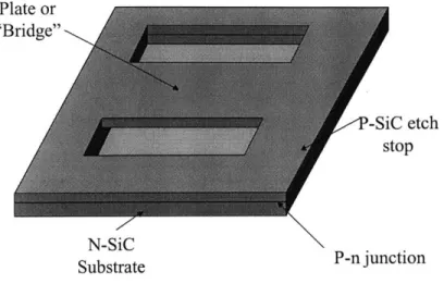
Figure 1.1: Basic design
develop SiC chemical sensors for common, commercial use. To make this device practi-cal, the development of an efficient thermal design is needed to reduce the power require-ments for a SiC chemical sensing device. This development work requires the exploration of different geometric configurations and the use of heat transfer analysis, both analytical and numerical, to optimize the performance of the SiC micro-sensor.
1.2 Basic Device Overview
SiC is a semiconductor material and can be doped with nitrogen (n-type) and with alumi-num (p-type). The n-type can be preferentially etched using a photochemical etch stop process developed by BMS to create a plate, or "bridge," as is shown in Fig. 1.1. When current is made to flow in the under etched plate, or bridge, resistive heating occurs, increasing the plate's temperature. Sensing film, such as a conductometric semiconducting oxide (eg. tin oxide), can be deposited on the top of the plate. This sensing film will react differently to different chemicals at different temperatures; this reaction is measured by changes in the electrical properties of the sensing film. For example, a tin oxide film is sensitive to reducing gases such as CO, H2, or acetone. At high temperatures the tin
Section 1.3: Project Objectives 19
oxide's conductance can be increased by as much as 25% by the presence and concentra-tion of CO, H2, or acetone. This conductance change occurs because of the absorption and
desorption of the chemical being sensed onto the tin oxide film [2], which effects the oxy-gen vacancy concentration in the film and hence its hole concentration. The correlation between electrical behavior and temperature with different films has been documented in work done by Semancik and Cavicchi [1] and will be discussed in greater detail later.
Improvements are made in the performance of the SiC micro-sensor by changing the design of the plate section. Heat transfer modeling is used to maximize the heating that will occur in the plate, minimizing power usage and heat losses. This work focuses on the plate section design and the thermal modeling of the micro-sensor.
1.3 Project Objectives
Design drawbacks existing in current chemical sensing technology determined several objectives for the plate design. These include manufacturability, electronics compatibly, temperature uniformity, fast time response, low power draw, and high operating tempera-ture. These requirements are the guidelines used for the designs described in this thesis.
Manufacturability of the sensor is the first design driver; the sensor must be designed within the constraints of current manufacturing capability. The sensor also must be designed to survive processing; steps in the processing, such as lithography, expose the chip to both high frequency and static loads. Reducing cost is an additional manufacturing concern. Fortunately, because of the high yield from each SiC wafer used to manufacture the hotplates, such micro electrical mechanical devices (MEMS) are relatively
inexpen-sive [5].
In addition to manufacturability, the SiC micro-sensor must be compatible with low cost electronics. Electronics are used to control the hotplate's temperature and heating
pr
characteristics, as well as sense the changes in conductivity of the sensing film. Expensive electronics would prohibit the use of micro-sensors as a replacement for the more costly sensors used today. Necessary to keeping the cost of electronics down is lower power, low voltage hotplates that are simple to operate.
Temperature uniformity over the hotplate is also crucial; assuring the chemical selec-tivity of the sensing film remains high. Since these measurements are dependent on equi-librium of oxygen vacancies in the film, it is critical that the temperature remain uniform over the sensing film [2]. To minimize this error an objective of less than 1% relative tem-perature variation over the plate is desired.
Time response is also important. Fast time response is important to quick sensor cycling, minimizing power requirements, and real time sensing capabilities. Response time is an important area for chemical sensor development in general, allowing for virtual real time information processing [5]. Applications such as combustion control require mil-lisecond sensor response times to allow active feedback based upon the sensing results.
Low power has a direct relation to low cost electronics; it allows for simple electronics and the use of common batteries. Many of the applications for this micro-sensor are remote sensing related, where the sensor operates off a battery and transmits sensor data. With such applications sensor life is important. A power efficient sensor can be operated with infrequent battery replacement. The objective of this project is to develop a sensor that operates on 50 mW or less, allowing it to operate off common, readily available, bat-teries.
The final requirement for such a sensor is high temperature capability. The plate should be designed to achieve temperatures of above 1300 K while minimizing the power required to achieve such high temperatures. The high temperature capability assures the sensor can detect most chemicals using the appropriate sensing films.
Section 1.4: Thesis Overview
These factors served as the design focal points throughout this work and will be used for comparison of the different designs.
1.4 Thesis Overview
This thesis is organized in a manner that follows the analysis steps taken during the design of this SiC sensor. The following chapter provides the basic background of micro-sensor operations. It then moves on to an analysis of the initial design, which is a simple plate, similar to the one shown in Fig. 1.1. The redesign will be focused on in Chapter 4, including a discussion of the analysis techniques used to model the designs. Chapter 5 will cover the design of tethers. Tethers are bridges used to hold the hotplate, reduce conduc-tive heat loss, and provide localized heating. Chapter 6 covers the final design of the sen-sor. An analysis, including experimental results, is then discussed evaluating the temperature dependent properties of SiC in Chapter 7, focusing on resistivity and thermal conductivity. Finally, the experimental tests of the sensor are analyzed and compared to the model results in Chapter 8, followed by conclusions and suggestions for design and modeling improvements.
The design and analysis of the hotplate will follow four major design changes and use both analytical and numerical solution techniques. Figure 1.2 shows the basic layout of these four designs and the progression of the designs from design 1 to design 4. Design improvements are achieved by the increasing heating in the tethers, reducing heat loss out of the plate, and using geometry to position heat generation in the most efficient areas.
22 Chan~ter 1: Introduction
Design 1: Bridge
(Origial Design) Design 2: Mini tethers
Design 3: Tethers Design 4: Necking
Figure 1.2: Basic design layouts
Chapter 1: Introduction
22
Chapter
2
Background
2.1 Chapter Overview
This chapter covers the operation of the SiC micro-hotplate designed for this project. It includes a description of the p-n junction used in this design, material properties, and the electrical contacts used in the device.
2.2 Material
The material chosen for the micro-sensor is silicon carbide (SiC). This material was cho-sen for many reasons, including its high operating temperatures and excellent thermal con-ductivity, as well as being a good semiconductor. The Cree company's single crystal 6H SiC [6] is used for this device. Some of the physical properties of this material are listed in Table 2.1.
Density
3.211g/cm321Specific
Heat 580 J/kgThemial Conducity 3.0-3.8 W/cm*
Bandgap 3.03 e
Resistivity Range (specific vakie dependent on doping):
N-type .04-.09 OHM-, P-type 1.0-5.0 OHM-cmn Table 2.1: SiC room temperature properties [6,7,8].
Many of the properties in Table 2.1 are temperature dependent and require some addi-tional analysis and experimentation to determine their properties as the hotplate heats to high temperature. The temperature dependent thermal conductivity and resistivity are important to the modeling of the designs discussed in this work. To account for this effect the temperature dependent properties are measured and discussed in the final chapters of this work. There the design of experimental structures to measure electrical resistivity and thermal conductivity as a function of temperature are discussed. These chapters also
include experimental results obtained from these devices.
SiC is an excellent semiconductor for high temperature chemical sensing because of its large band gap, good electrical conductivity, and high operating temperature. SiC is a
wide energy band gap material, with a band gap of 3.03 eV [6]. This wide band gap allows
SiC to operate at high temperatures without suffering from intrinsic conduction effects, which cause a significant decrease in electrical resistivity. It is approximated that at tem-peratures above 1800 K [10] SiC begins to behave intrinsically, exciting valence band electrons into the conduction band and causing the decrease in resistivity. The wide band gap also allows the electrical properties of the SiC to be controlled by doping. This allows currents and voltages to be optimized for the electronics being used to control the micro-hotplate. It is these properties that make SiC an excellent choice for these micro-sensors.
2.3
P-n Junctions
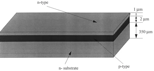
The SiC sensors discussed here are fabricated from a three-layered SiC wafer. The wafer consists of a p-layer and a n-layer on a n-substrate (see Fig. 2.1). The substrate has a
Section 2.4: Chemical Sensing 25
n-type
1gm
350 gm
n- substrate p-type
Figure 2.1: Structure of unetched wafer
ness of 350 gm, the p-type layer is 2 gm thick, and the top n-layer is 1 gm thick. The top p and n-layer SiC serve as part of a proprietary sensor transduction mechanism developed by BMS with the top n-layer used as a heater. The p-n junction between the top n and p layers electronically isolates the top layer, allowing electricity to conduct through the n-layer without current leakage to the underlying n-layers. The n-substrate provides support for the micro-hotplate.
2.4 Chemical Sensing
A critical aspect of a SiC chemical sensor is the films used for sensing. Typical micro elec-trical mechanical system (MEMS) sensors use oxides to detect physical, chemical, and biological characteristics of different chemicals. Oxides exhibit a wide range of properties which make them useful for measuring the mechanical and biological properties of differ-ent substances [5]. Chemicals can be detected by a variety of methods, including electrical resistivity, mechanical deflection, resonance principles, capacitance changes, or calorimet-ric effects [1]. The electcalorimet-rical resistivity method will be the method used for the sensor developed in this work. The method entails measuring the changes in the electrical
tivity of the sensing film with changes in temperature, and correlating the changes to the presence of specific chemicals. This method has also been called conductometric sensing [1]. The micro-hotplate designed in this work serves as a platform for heating the sensing films to their operating temperatures.
Absorption of molecules onto the surface of the sensing film and diffusion of oxygen into and out of the film's interior are the main mechanisms for conductometric sensing; this absorption and diffusion cause changes in the electrical conductivity of the film. Increasing temperature causes change in the partial pressure of oxygen, increasing oxygen vacancies or interstitials sites [5]. This allows the absorption of chemicals, creating donors and acceptors. The addition of donors or acceptors changes the electrical conductivity of the sensing film, which can be measured and correlated to the chemicals present in the measured gas. Materials that are dependent on changes in their bulk resistances must either be highly porous or heated to high temperature in order to assure adequate diffusion
[9].
A high level of selectivity is required in sensing films in order to be able to distinguish between several different chemicals and to determine amounts present. Two methods are used to achieve this selectivity, "materials selectivity" and "kinetic selectivity." Materials selectivity is using compositionally different films to detect different chemicals and prop-erties [1]. Developing a picture of the chemical make-up of a gas is completed by compar-ing the reactions between different films. Kinetic selectivity uses rapid heatcompar-ing of the films and measures resistive changes in relation to rapid changes in the temperature. This response can then be correlated to the type and the amounts of the chemicals present [1]. Use of arrays of different types of sensors can be used in either case to allow greater selec-tivity.
Section 2.4: Chemical Sensing 27
Figure 2.2: Programmed temperature response of a tin oxide micro-hotplate to a series of organic vapors (from NIST) [1]
Figure 2.2 shows the measurement capabilities using kinetic selectivity. The device used to obtain these results is a silicon based device with a SiO2 substrate and a coil heater developed by NIST [1]. On top of this device is deposited a tin oxide sensing film [1].
Contacts are attached to the sensing film to measure the change in electrical properties. Figure 2.2 represents an example of measurements made during a testing of the tin oxide sensing film. The test involves introducing the sensor to several different chemicals and measuring conductance of the tin oxide over several, ramped temperature sweeps. The temperature is ramped up over time to a peak, then the device is cooled, and the tempera-ture is ramped again. This cycle is repeated, producing the heating pattern shown in the Fig.2.2 by the temperature bars across the horizontal axis. The results show the correlation between temperature and conductance in relation to several different chemicals, as well as the repeatability of the results. Each different chemical has a clear and distinct effect on the tin oxide's conductance as the tin oxide is heated over time. This change in
tance can be correlated to type and amount of chemicals present. This measurement tech-nique has been developed and tested by the National Institute for Standards and Tests (NIST).
2.5
Conclusions
The measurement techniques developed by the NIST using Silicon Oxide heaters and dif-ferent sensing films can be applied to SiC based micro-hotplates to make micro-sensors. These SiC based micro-hotplates are expected to out perform the Si02 used by NIST because of the superior high temperature properties of SiC. Further performance improve-ments can be gained by thermally modeling the SiC micro-hotplates and using the hot-plate's geometry to optimize the performance of the plate, and is the focus of this thesis.
Chapter
3
Initial Design Analysis
3.1 Chapter Overview
Prior to this research, Boston Micro Systems fabricated and tested a very basic initial hot-plate design for chemical sensing applications to verify the manufacturing techniques and processes necessary for SiC micro-sensor development. The device performed poorly, however, due to contact overheating. In this chapter, an analysis of this initial design is discussed that will serve as a baseline for follow-on designs and improvements. In addi-tion, this chapter will cover the layout and the geometry of the device. A discussion of the device's advantages and its drawbacks is included; design improvements are identified for
further analysis in later chapters.
3.2 Geometry
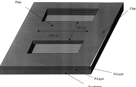
The geometry of BMS's original device is a simple plate that consists of a 200 x 200 jim bridge-like structure as shown in Fig. 3.1. The design uses a p-n junction material with a n-type substrate, a p-type middle layer, and a n-type top layer. The n-substrate is removed from below a 200 x 200 jim region of the top p and n-layers leaving a suspended bridge. The bridge section is referred to as the plate and the whole device is called the chip.
30 Plate Chip N-Layer P-Layer N substrate
Figure 3.1: Initial plate design
3.3 Modeling Assumptions
A simple analysis of the initial plate design can be performed analytically. Several key assumptions are made to develop this simple model. The first is that convective heat trans-fer to the air surrounding from the plate is negligible. This can be shown using Newton's
law of cooling [11],
q" = h(Ts -
Tinf)
(3.1)where h is the convective heat transfer coefficient, TS is forced convection, and Tinf at is the temperature of the surrounding air. Typical heat transfer coefficients to the air range from 10 W/m2-K for natural convection to 1000 W/m2-K for forced convection. For forced convection, assuming the surrounding air is at room temperature (with h=1000 W/ m-K) and the surface temperature of the plate is 1000 K, q" is 701,000 W/m2. When con-sidered with the size of the plate the heat transfer loss is only 0.028 W. In the more
31
able natural convection case the heat transfer loss is 0.00028 W. For comparison to conduction, assume that the center of the plate is operating at 1000 K and the ends are at room temperature. Assuming one-dimensional heat conduction the conductive heat trans-fer can be calculated using
q = kA (3.2)
dx
where, k is the thermal conductivity and A is the cross-sectional area. The heat transfer due to conduction, using the cross sectional area of the plate, is 1 W. That is two orders of magnitude greater then the high speed flow case, and four orders of magnitude greater then the low speed flow case. Based on these results convective effects can be neglected in the modeling. This assumption is carried through the analysis of all of the designs. The small size of the plate causes conduction to be the dominant effect since the surface of the plate is too small for convection to become a significant factor.
The ends of the plate are assumed to be at room temperature for this analysis. This assumption is reasonable because the chip is significantly larger, 100,000 times larger, than the plate and is thus able to absorb the heat lost from conduction out of the plate. In a more sophisticated finite element model discussed later the validity of this assumption will be shown (see Chapter 5).
The thermal and electrical properties are also assumed to be temperature independent. This assumption, while reasonable for basic analysis, cannot be maintained in more accu-rate models since both electrical and thermal properties are highly dependent on tempera-ture. As such, an entire experiment has been developed to determine the thermal and electrical conductivities for doped SiC in relation to temperature (see Chapter 7). Since the thermal conductivity of SiC decreases with increasing temperature the power required to heat the hotplate will improve as temperature increases [10]. It can therefore be assumed
32 Chapter 3: Initial Design Analysis
that this assumption will represent a worst case scenario for the plate performance. In later iterations, this assumption will be replaced with reasonable temperature dependent proper-ties found from the experimental results.
One final significant assumption is that the electrical current flow through the plate is uniform. No local heating effects in the plate due to non-uniformities will be considered in the modeling of the hotplate. This is a reasonable assumption considering the size of the plate as well as the excellent thermal conductivity of the SiC. The high thermal conductiv-ity in SiC, especially at high temperatures, tends to smooth the temperature distribution. In Chapter 6, where the final necked design shown in Fig. 1.2 is analyzed, this assumption will be discussed further.
Internal resistive heating is the mechanism used to obtain high temperatures. For this analysis resistance becomes a critical factor for producing the heat in the plate; the plate section has a resistance of 890 Ohms. Using these assumptions the model of the plate can now be discussed.
3.4 Performance Analysis of Original Design
With these assumptions the initial plate design is analyzed using both analytical methods and finite difference methods. The hotplate is first analyzed analytically using Poisson's equation for heat diffusion with a source term and a constant thermal conductivity [11],
-4
= kV 2T (3.3)where q is the internal heat generation per unit volume and k is the thermal conductivity. A one-dimensional solution of this equation is of the form
T = -_j - x2 + A - x + B (3.4)
2k
condi-tions of the plate.
The boundary conditions used to find A and B are calculated from the assumption that the chip is at room temperature. At both ends of the plate, where x is zero and x is L, the length of the plate, the temperature will be Trt = 298.15 K. Using these boundary condi-tions A and B are calculated to be
A =4
2k (3.5)
B = rt The solution is now written as
T = --
1-x2+SI
- x+T (3.6)2k 2) t
-The value q is an important aspect of this equation since it determines the effect of the internal heating on the temperature distribution. It is calculated from the following:
. 2
q 2 2 - (3.7)
t w
Equation 3.7 is based on the power produced by resistive heating per unit volume. In Eq. 3.7, p is the resistivity of SiC, I is the current in the plate, and t and w are the plate's thick-ness and width, respectively. The temperature distribution as a function of position given
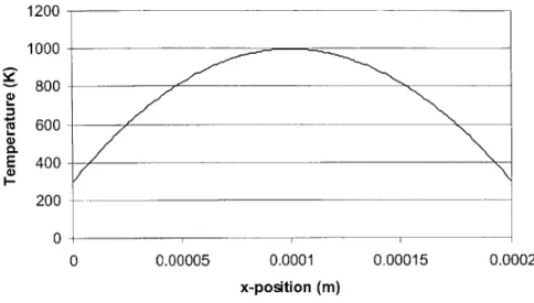
in Eq. 3.6 is plotted in Fig. 3.2 for values of k = 230 W/m-K, q = 3.12 x 10¹³ W/m3, L
-200 pm, and w = -200 gim. Under these conditions, the total power dissipated in the plate is 1.3 W. The plot in Fig. 3.2 is an inverse parabola and show the large temperature distribu-tion over the plate.
Following this work, a more sophisticated two-dimensional model was developed using a finite difference method. This method involves dividing the plate up into several 2-d squares and using boundary conditions to average each point in the grid with it sur-33 Section 3.4: Performance Analysis of Original Desig
34 -E 0 1200 1000 800 600 400 200 0 0 0.00005 0.0001 x-position (m) 0.00015 0.0002
Figure 3.2: Analytical temperature distribution over the initial plate design
rounding points. By iterating the solution between each successive step the error decreases to a set size. The plate was broken up into a grid of 10,000 2 x 2 jim squares. Using such a
grid a model can be developed using Eq. 3.8 and Fig. 3.3 [11],
T = Tm,n+1+Tm,n-1 +m+1,n m-1,n (3.8)
m, n
4-Due to the electrical current flow through it, the plate is internally heated, so an additional term must be added to account for this heat generation,
P
AT n - (3.9)
ml,n t -k
where P represents the power introduced by each individual 2x2 jim element in the grid due to resistive heating and t is the plate thickness, which is 3 jim for this case. This gives the following for the finite difference model:
T - Tm, n + 1+ Tm, n- 1 + Tm+ 1, n + T im- 1, n + P (3.10)
mn, n 4 t -k.
The power is determined by calculating a power density for the device by taking the entire plate resistance times the square of the current and dividing by the plate's volume. If, as it
Section 3.5: Conclusions m, n+1 A y m, n m-1, n 4± m+1, n A x m, n-1
Figure 3.3: Interior grid designations for finite difference method
is assumed, current density is uniform, the power is the power density times the volume of each, individual, element. For the plate being modeled there is a power density of 3.23 x 10¹³ W/m3, producing an elemental power generation of 0.000129 W. A further discus-sion of this modeling technique can be found in Appendix A. It includes a discusdiscus-sion of equations and methods used to calculate edge effects and including boundary conditions in the analysis.
The data was entered into an ExcelTM spreadsheet and iterated using the ExcelTM cal-culation feature until the error was less then one thousandth of a degree. The error is calcu-lated by ExcelTM by taking each node's temperature for the prior iteration and comparing it to the current iteration. Once the difference between the two iterations is less then the set error value of one thousandth of a degree the calculation is stopped, displaying the results. The results of this calculation are in Fig. 3.4. These results match the results from the ana-lytical analysis, with a power requirement of 1.3 W.
3.5
Conclusions
Several observations can be made about this design. First, this design requires a very high power to operate at 1000 K. At such a high power consumption, the chip is not practical
36 Temp (K) * 900-1000 0800-900 0 700-800 0600-700 0500-600 0 400-500 IM300-400
Figure 3.4: Temperature distribution over plate
for use in the applications discussed earlier and would have little advantage over existing systems. The high power consumption comes from significant thermal contact between the plate and chip, which allows significant conductive heat loss into the large surrounding
chip.
A second concern of such a design is a lack of temperature uniformity. The tempera-ture variations over the plate covers temperatempera-tures from 298 K to 1000 K. Such a variation of temperature prevents the measurement of the sensing films conductivity from being accurate. With this temperature distribution the design does not meet the temperature uni-formity requirements set forth earlier in the work.
The failure of the design in testing can be attributed to the small contact pads used to make electrical connections between the device and the controlling electronics. These contact pads, due to their smaller size and geometry, have a electrical contact resistance comparable to the plate. Because of the high power needed to heat the plate the contacts will also heat, and their large resistances will cause them to heat to high temperature, degrading the electrical contacts and ultimately destroying the device.
Chapter
4
First Design Iteration
4.1 Chapter Overview
This chapter will look at some design modifications made to improve the performance of the initial plate design. The most important and significant change made minimizes the conductive heat loss from the plate to the chip. A detailed description of the change will be discussed as well as a detailed analysis of the performance of the new design. Advantages and disadvantages will be delineated for further design improvement.
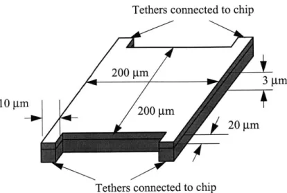
4.2 Geometry
The next design is shown in Fig. 4.1. The center plate is 200 x 200 tm and is attached to the rest of the chip by four 20 im long, 10 gm wide, tethers, one in each corner. Since this new geometry reduces the contact area between the plate and the chip by a factor of 10, the conductive heat transfer out of the chip is expected to be significantly less then in the previous design.
Chapter 4: First Design Iteration
Tethers connected to chip
200 Rm 3
10 RM 200 Rm
20 Rm
Tethers connected to chip
Figure 4.1: First design iteration (plate section only)
4.3 Modeling Assumptions
A finite difference model was used to analyze this design. The assumptions used in this
model mirror those applied to the model discussed in Chapter 3. The convective heat
losses are assumed negligible, the current density, and hence heating, is assumed uniform,
and the surrounding chip is assumed to remain at room temperature. The surrounding
boundary condition is applied to the chip end of the tethers that connect the plate to the
chip.
Internal heat generation is calculated separately for the tether sections and the plate
section. Each of these sections will have a different resistance determined by their
geome-try. The resistivity of n-type Si-C doped at 10-19 cm-
3, as is used for this modeling, is
0.00089 Ohm-in [6], thus producing a resistivity for the tethers of 1780 Ohms each and a
resistivity for the plate of 890 Ohms. This significant difference in resistivity is a critical
factor in this and later designs. It causes most heating to occur in the tethers as current is
passed through them, into the plate, and out the opposing tether. The final important
11 R
assumption, as was made in Chapter 3 for the plate design, is that the material properties of the SiC do not change with temperature.
4.4 Performance Analysis of First Iteration Design
For the finite differencing model of this new hotplate design 2x2 gm elements were used to develop the finite differencing grid. The internal heat generation used in Eq. 3.9 will be different between elements used in the tethers and elements used in the plate. The power generation will be based on resistances calculated from the tether and plate geometries. Grid elements modeling the tethers will have the power produced from the tethers resis-tance, and grid elements modeling the plate will have power produced from the plate resi-tance. Equation 3.10 was used to calculate the results and the edge effect equations
discussed in Appendix A.
The results are obtained from ExcelTM after running the iterative calculation option until the error between each successive step is less then one thousandth of a degree (see Fig. 4.2). The current required for the plate was found to be 0.011 A, in order to achieve a peak temperature of 1000 K. Thus, the operating power of the design is 0.309 W, an order
of magnitude improvement over the design discussed in Chapter 3. The power dissipated in each of the tethers is 0.051 W, and 0.103 W for the plate; power for all four tethers is
0.206 W, or twice as much as the plate. The temperature distribution of this design can be
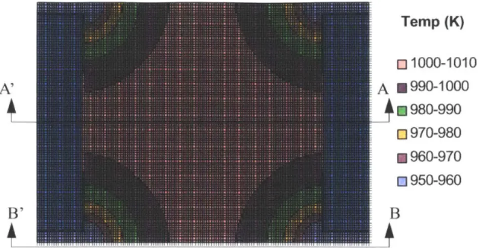
seen in Fig. 4.2. In this picture only temperatures from 950 K to 1010 K are shown, the peak temperature is shown in the diamond shape center region and is approximately 1000 K. Temperature distribution is improved over the previous design, as well the required operating power to achieve temperatures of 1000 K. Figure 4.3 shows the temperature dis-tribution of the plate along a line AA' in Fig. 4.2, and along a line BB'.
39
Chapter 4: First Design Iteration 40 B' Temp (K) 3 1000-1010 A 0990-1000 m 980-990 E 970-980 0 960-970 m 950-960 B
Figure 4.2: Temperature distribution over plate of first design iteration
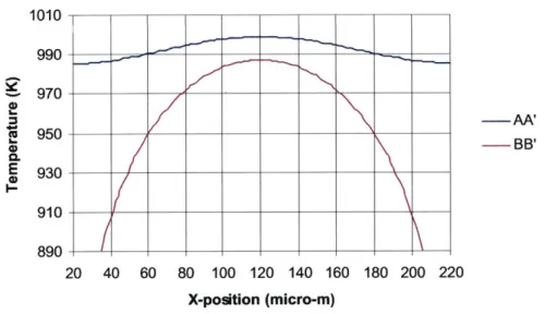
CL E CD 1010 990 970 950 930 910 890 AA' -- BB' 20 40 60 80 100 120 140 160 180 200 220 X-position (micro-m)
Figure 4.3: Temperature distribution over the plate center and plate edges respectively
Figure 4.3 shows that the temperature distribution is much improved over the previous design. In the previous design the distribution was an inverted parabola and the tempera-ture ranged from 298.15 K to 1000K. The distribution over the center of the plate for this tether design is less then +/- 20 degrees, but is still over 100 degrees for the edges. This is
Section 4.4: Performance Analysis of First Iteration Design Temp (K) l 1000-1010 A'A M990-1000 o9980-990
o
970-980 * 960-970o
950-960B'B
Figure 4.4: Temperature distribution over 40 gm tether design
an improvement, but still does not meet the goals outlined in Chapter 1, requiring a 1% relative temperature variation over the plate, or +/-10 degrees for a plate at 1000 K. The
improved distribution can be attributed to SiC's excellent thermal conductivity coupled with the heat generation in the tethers. This allows the heat generated from the much
higher power dissipating tethers to distribute to the rest of the plate.
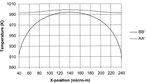
From these results it can be concluded that lengthening the tethers, thus increasing the resistivity of the tethers, improves the heating of the micro-hotplate. An analysis of a model using 40 prm tethers instead of 20 pm tethers gives the following changes and improvements. This increases the resistance of each tether to 3560 Ohms each, producing an overall resistance of 4450 Ohms for the entire plate and tether combination. A current of 0.007 A will heat the center of the plate to 1000 K. At this current the total power draw of the device is 0.218 W, a ten fold improvement over the shorter tethers. Each tether dis-sipates 0.0436 W, and the plate draws the same 0.0436 W as in the shorter tether design. Thus, the tethers as a whole dissipate four times the power as that in the plate, or 0.1744 W. That is a doubling of the ratio of heating power between tethers and plate from the shorter tether design. Figure 4.4 shows the temperature distribution over this design. The
42 Chapter 4: First Design Iteration 1010 990 970 -BB' 950-1~ -AA' C)0. 930-910 --890 40 60 80 100 120 140 160 180 200 220 240 X-position (micro-m)
Figure 4.5: Center and end temperature distribtuion for 40 grm tethers
high temperature zone, those areas close to 1000 K, is much larger then in the previous short tether design. The center, along line AA' in Fig. 4.4, and edge, along line BB', cross-section temperatures can be found in the Fig. 4.5. The temperature distribution over the plate for this design is closer to +/- 50 degrees, a two fold improvement over the shorter tether design.
4.5
Conclusions
The performance improvements of the tether design over the initial design are significant for several reasons: power improvements, temperature uniformity, and heating efficiency. First, there is an order of magnitude reduction in the power required to achieve 1000 K between the tether designs and the design discussed in Chapter 3. This improvement is made by decreasing heat loss from the plate and providing heating from the more power efficient tethers. Temperature uniformity is also greatly improved, improving sensor
reli-ability.
Chaoter 4: First Design Iteration
Section 4.5: Conclusions 43
This work suggests that lengthening the tethers will result in improved thermal perfor-mance: however other concerns must be considered, such as packaging, structural stabil-ity, and electrical performance. These factors will be considered in the designs discussed in the following chapters.
Chapter
5
Second Design Iteration
5.1 Chapter Overview
Now that tethers have been identified as a important design feature, this chapter will ana-lyze different tether designs, optimizing the sensors performance with respect to design variable such as length, width, and geometry. First, an analysis of tether length is pre-sented, and secondly consideration of the geometry of the tethers is discussed. New analy-sis techniques are utilized including the use of finite element modeling (FEM) and the FEM program ADINA. FEM provides a more accurate solutions to the model as well as being more computationally efficient then finite differencing techniques. A discussion of FEM methods will be included as it pertains to this modeling. Further discussion of this method can be found in Appendix B.
5.2 Geometry of Long Tethered Plate
As shown in Fig. 5.1, the plate is 200 x 200 km. It is now supported by four 240 gm long, 10 gm wide, tethers sections that connect the plate to the chip. These tethers are "wrapped" around the plate to help prevent failure when the plate is fatigued or stressed due to thermal expansion.
46 Tethers connected to chip 10 tm /200m3 9m Tethers onnected to chip 200 gm tethers
Figure 5.1: Long tether design layout
This spider like design is advantageous because it helps to minimize stress in the tethers and should prevent the chip from buckling or bending from thermal expansion induced stresses. The material composition is the same as in previous design, with a n-substrate, a p-layer, and a top n-layer. The p and n-layer remain in the hotplate section while the
n-sub-strate is removed underneath this section.
One geometric consideration of the plate design is the stress placed on the plate during manufacturing. This was not a concern in previous designs, but as the tethers length increases it becomes a greater issue. During the processing there are photolithography steps where the device is spun at approximately 3000 rpm. The sensor needs to structur-ally survive during this processing phase. To perform a simple structural analysis, the 240 gm tethers are treated as individual cantilevers with a force loading at their ends of approximately one quarter of the weight of the center plate. Using a modulus of 450 GPa for SiC [12], an end deflection of the device can be calculated and checked. The moment
Section 5.3: Modeling Assumptions and Calculations for Long Tethered Plate
of inertia is calculated using the equation for a rectangular cross-section [13]. A deflection
of 3.58 x 10⁻⁴ tm is calculated for a load of 9.15 x 10⁻¹⁰N, which represents the force of
the weight of the plate. This is a small deflection and leaves plenty of clearance between the plate and surrounding chip. The natural frequency of the tethers is also calculated using these parameters and is found to be 165.5 KHz, which is well above the 3000 rpm, or 50 Hz, loading the photolithography processing step produces.
5.3 Modeling Assumptions and Calculations for Long Tethered Plate
Two techniques are used in this analysis for modeling the long tether hotplate design. The first is an analysis using the same finite differencing method as used previously. The assumptions used for the short tether hotplates still apply, including room temperature boundary conditions at the end of the tethers, non-temperature dependent properties, and no convective heat loss. The ends of the tethers, where they make contact with the chip, are still assumed to be at room temperature. The power inputs for each tether are recalcu-lated to accommodate the longer tethers. The resistance of the tethers increase to 21360
Ohms each by taking 0.00089 Ohms-in times the tether length of 240 im, and divided by
the cross-sectional area of 10 mi2. This resistance is a 10 fold increase over the shorter tether designs. The plate resistivity will remain at 890 Ohms since its geometry has not changed.
The second analysis is completed using finite elements and ADINA, a FEM modeling program [14]. A finite element model is a more accurate and efficient model then the finite difference model. While finite differencing is an ideal system for modeling simpler struc-tures, with its simplicity and ease of use, it becomes cumbersome with added structural complexity, and loses accuracy. A FEM approach using a program such as ADINA is a much more accurate and robust method compared to that of finite differencing.
48 Catr5 eodDsg trto
A FEM model is based on the "principle of virtual work". This principle states that for the equilibrium of a body it is required that for any small virtual displacements, in this case changes in temperature, the total internal virtual work must equal the external virtual work. This statement can be shown in the following equation:
,Tko'dV =
5qBdV+
0s sdS+Q
(5.1)V V S
Eq. 5.1[15] is the "principle of virtual temperature", since it is the heat transfer representa-tion of the "principle of virtual work". The right hand side represents the external virtual work, and the left hand side represents the internal virtual work. 0 represents the tempera-ture, and the bar over 0 represents the virtual temperature distribution being considered. V represents the integration over the volume of body being considered, such as in Figure 5.2, and S represents the surface. The internal heat generation is represented by qBand the heat flow into the body is qs.
Q'
represents the concentrated heat flow inputs, and is actually neglected for this analysis because the only heat flow is internally generated. 0' is the rep-resentation of the change in temperature with change in position. The thermal conductivity matrix is represented by k.The "principle of virtual temperature" refers to virtual temperature changes in the body, but do not represent actual temperature changes. Virtual temperatures are a thought experiment used to establish the equilibrium equation in Eq. 5.1 [15]. If the correct 0' is known, then Eq. 5.1 holds true for any arbitrary virtual displacement that is continuous and has the same prescribed boundary conditions as the body. If 5.1 is not true in such a case, the 0' is not the exact temperature changes in the body. The concept of virtual tem-peratures and virtual work is a rather complex subject, and since it is not the focus of this work will not be discussed further. For more detailed explanations and discussion of this
Chapter 5: Second Design Iteration
Section 5.3: Modeling Assumptions and Calculations for Long Tethered Plate 49
Surface
4- node
09'
Figure 5.2: Fintie element breakdown
concept readers are referred to Bathe and Bucahanan's works [15, 16], or any other FEM text. The "principle of virtual temperature" will become important in the next section.
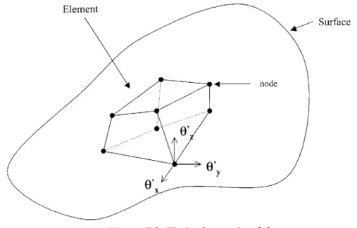
First, to understand the FEM analysis in this work, the important assumptions and their effect on boundary conditions, the basic model construction must be explained. Any body can be divided up into many different elements. Figure 5.2 shows a body and one
element in the body.
The body has boundary conditions and loadings placed on it to fit the object being modeling; in the case of the hotplate these are in the form of temperature boundary condi-tions placed on the chip's edges. The body is then approximated using many of these ele-ments put together by a process called meshing. The eleele-ments can have any shape, although there are some efficient meshing techniques that will be discussed later. Each element is made up of nodes and each node has a displacement, in this case a temperature and temperature change, associated with it. For heat transfer, several other factors can also be included, such as heat transfer through conduction, convection, and radiation. These elements put together make up the body of the device, the hotplate for this modeling.
For each element m, the following set of equations [15] are true:
0(m) - (m)g (5.2)
eS(m) _ S(m)g (3)
6(m) (m)g . (5.4)
The temperature vector on the right hand side of these equations represents the matrix of all nodal point temperatures. H is the element temperature interpolation matrix, B is the temperature gradient interpolation matrix, and HS is the surface temperature interpolation matrix. These matrices are critical for solving for the temperature changes in the body. Before solving for the temperature from these equations the boundary condition tempera-tures are applied, the edges of the chip are at room temperature. Substituting these equa-tions into Eq. 5.1 and simplifying yields Eq. 5.5, which represents the relation between heat input and temperature for each node. The virtual temperatures assumed for this
analy-sis are simple unit temperature changes.
itk c e (5.5)
Appendix B contains a detailed explanation of the calculation performed to obtain Eq. 5.5. Kk is the conductivity matrix and is formed from the temperature gradient interpolation matrix and the matrix k, which is the thermal conductivity properties of the material (see Appendix B). Matrix k is a simple matrix made with the thermal conductivity value of SiC placed along the matrix's diagonal. K' is the convection matrix, and is neglected for this calculation since convection is ignored because of its negligible effect, as in previous cal-culations.
![Figure 2.2: Programmed temperature response of a tin oxide micro-hotplate to a series of organic vapors (from NIST) [1]](https://thumb-eu.123doks.com/thumbv2/123doknet/14685348.560115/27.918.272.614.176.485/figure-programmed-temperature-response-hotplate-series-organic-vapors.webp)