Design of Resonant-Tunneling Diodes
for a GaAs Integrated SRAM
by
Rajni J. Aggarwal
S.B., S.M., Massachusetts Institute of Technology (1990)
Submitted to the
Department of Electrical Engineering and Computer Science
in partial fulfillment of the requirements for the degree of
Doctor of Philosophy
at the
MASSACHUSETTS INSTITUTE OF TECHNOLOGY
February 1996
@ 1996 Massachusetts Institute of Technology
All rights reserved
Althor
Certified by_
.~...r~CV~..
v
"-•--
ce
cnber 18, 1995
,
G. Fonstad, Jr.
..,,cal Engineering
.sis Supervisor
Accepted
by-AOFATCHNOLGY OF TECHNOLOGYR. Morgenthaler
/
Chairnaan, Committee on Graduate Students
APR 1 1 1996
LIBRARIES
Design of Resonant-Tunneling Diodes
for a GaAs Integrated SRAM
by
Rajni J. Aggarwal
Submitted to the Department of Electrical Engineering and Computer Science on December 18, 1995, in partial fulfillment of the
requirements for the degree of Doctor of Philosophy
Abstract
The resonant-tunneling diode (RTD) has frequently been cited as a potential building block for high speed, low complexity circuits. This work investigates the application of RTDs in a SRAM. The effects of six design parameters on memory switching speed and static power are evaluated and design rules for a two-RTD one-EFET SRAM cell are established. A novel integration technique, Epitaxy-on-Electronics (EoE), enables the integration of high performance relaxed-buffer In.Gal_,As/A1As RTDs on commercial GaAs circuits. A variety of relaxed relaxed-buffers and relaxed-buffer RTD (RBRTD) structures were investigated. We conducted a study of several grading methods at MBE growth temperatures suitable for EoE and found that the threading dislocation density of the RBRTDs is relatively immune to the indium grading profile. RBRTDs grown on integrated circuits (IC) and epi-ready substrates (ERS) were compared. Greater relaxation was observed in the material grown on the IC. RTDs integrated on the IC had lower current densities than those grown on the ERS. This reduction is attributed to the presence of misfit dislocations in the RTD barrier/well interfaces which are depleting the RTD, effectively reducing the RBRTDs electrical area. Integrated RBRTD-EFET SRAM cells were designed, fabricated, and a proof-of-concept SRAM cell was successfully demonstrated.
Acknowledgments
Despite the frustrations of research and the climate and atmosphere of New England, I can honestly say that I did enjoy some parts of this experience. The enjoyment has come from my interactions with the people around me. I appreciate all of their efforts toward my continued success. A few, in particular, deserve special thanks.
I would like to thank Prof. Clif Fonstad for giving me the opportunity and support to explore many research avenues. He has taught me to define a problem and identify the potential of each of its many solutions. Though focused on RTD circuits by the nature of the graduate process, these skills will serve me for the duration of my career. I appreciate the time invested by Prof. Charlie Sodini and Prof. Alan McWhorter in providing additional guidance for this work.
I am very grateful to my collaborators Prof. Eugene Fitzgerald and Mayank Bulsara. Their help was an integral part of the success of this project. Our interaction was more enjoyable than I can properly convey - we combined fun, learning, and addictions to Jolly Ranchers.
As with any research performed with shared experimental facilities, many thanks are owed to past and present members of my research group. I am forever indebted to Prof. Woo-Young Choi, Dr. Jurgen Smet, and Dr. Krishna Shenoy for their patience in helping me conquer the demons of the MBE lab. I appreciate all the support given by Paul Martin, Janet Pan, Hao Wang, Yakov Royter and Norio Iizuki. Without their help, the Monster would not have yielded samples of any worth. I appreciate the smiles and sympathetic ear of Isako Hoshino. Sheila Prasad was always there with professional and personal words of wisdom. And special thanks to Joe Ahadian and Steve Patterson for their encouragement, support, and friendship, especially during the last few months of this work.
My interest in III-V heterostructures was sparked as a VI-A student at Texas Instruments. I credit all members of the Advanced Concepts Branch for nurturing that spark. In particular, Dean Collins has had a hand in all of my personal and professional successes. John Randall and Jim Luscombe have provided support, friendship, and advice for the last eight years.
There are a few people at MIT who have crossed the line from professional colleague to life-long friend. J.P. Mattia is one of them. J.P., I will be forever amazed by your depth of knowledge and breadth of interests. You make physics fun, be it in an office or on top of a mountain in New Hampshire. Thanks for listening to my mindless drivel and turning my dumb questions into profound statements. Krishna Shenoy started out as an officemate and somewhere between "Cosmetic Pink" and "Sandy Pebble" he turned into a soul mate. Krishna, thank you for always being there for me.
My family has provided immeasurable moral support throughout my graduate career. My parents often heard the worst, and seldom heard the best. I can't thank them enough for their love and encouragement throughout my entire education. Nell and O.H., thanks for your prayers; they helped even if you didn't know a specific prayer to make RTDs work. Mala and Matt, you can stop making fun of me now - I am FINALLY entering the real world! And, I would
6
never have finished without the help of my husband, Michael. He has pulled me through the lows and helped me celebrate the highs of graduate school. Michael, everything this document represents is a testament to your perseverance and love.
Contents
1 Introduction 15
1.1 Monolithic RTD-based SRAMs ... 16
1.2 Thesis Organization ... 17
2 RTD-EFET SRAM 19 2.1 Operation of an RTD-EFET SRAM ... 19
2.2 Static Power of an RTD-EFET SRAM ... ... 23
2.3 Switching Current of an RTD-EFET SRAM ... 26
2.4 Switching Speed of an RTD-EFET SRAM ... 27
2.4.1 SRAM Model Description ... ... 28
2.4.2 Effects of PVCR ... ... 31
2.4.3 Effects of Current Density ... ... 34
2.4.4 Combined Effects of PVCR and Current Density ... 36
2.5 Desired RTD Characteristics for an RTD-EFET SRAM ... 38
3 RTD-MESFET Circuit Design and Fabrication 41 3.1 Epitaxy-on-Electronics Integration Technique ... 41
3.1.1 RTD-MESFET Circuit Design ... 43
3.1.2 MESFET Circuit Fabrication ... ... 43
3.1.3 MBE Heterostructure Growth ... 44
3.1.4 RTD Fabrication ... ... 45 3.2 W ellA rray ... 46 3.3 SRAM Cells ... 48 3.4 Memory Array ... ... ... 55 3.5 Circuit Summary ... ... ... 62 3.6 MIT-OEIC-3 Features ... 63 3.6.1 Conversion Errors ... 64 3.6.2 Implanted vs. Nonimplanted DGWs ... ... 64 3.6.3 DGW Cleaning Problems ... 65
CONTENTS
4 Relaxed-Buffer RTDs 67
4.1 Relaxed-Buffer RTD Materials ... 67
4.2 Mechanisms of Strain Relief in Relaxed Buffers ... 73
4.3 Relaxed-Buffer Demonstrations ... 75
4.4 EoE-Compatible Relaxed Buffer Quality ... 76
4.4.1 Effect of Grading Method on Relaxation ... 78
4.4.2 Effect of Grading Method on Dislocation Density ... 85
4.5 High-PVCR RBRTD ... ... 96
4.6 Series Resistance of RBRTDs ... 98
5 Characterization of Monolithically Integrated RBRTDs 105 5.1 Material Characterization of Integrated RBRTDs ... 106
5.1.1 IC Substrate Quality ... 106
5.1.2 IC Epitaxial Material Quality ... . 107
5.2 Degradation of IC Electronics ... 113
5.3 Electrical Characterization of Integrated RBRTDs ... 115
5.3.1 Effect of Substrate on RBRTD Performance ... 116
5.3.2 Performance of Well Array RBRTDs ... 124
6 Characterization of RTD-EFET SRAM Circuits 127 6.1 Monolithic RTD-EFET SRAM Circuits ... ... 127
6.2 Hybrid RTD-EFET SRAM Circuits ... 130
7 Conclusions 137 7.1 Accomplishments ... 137 7.2 Future W ork ... 140 7.2.1 Integration Studies ... 140 7.2.2 M aterials Studies ... 141 7.2.3 Electrical studies ... 141
A RTD-EFET SRAM Analytic Model 143
B Documentation for RTD-OEIC-1 149
C Integrated RTD Process Flow 161
D RTD-EFET Ring Oscillator 165
List of Figures
2-1 Circuit schematic of the RTD-EFET SRAM cell... 2-2 Operation of the RTD-EFET SRAM cell ... 2-3 Load line characteristics as a function of VRTD. . ...
2-4 Measured voltage bistability of an RBRTD storage element ...
2-5 Measured Iswitch,min requirements for an RTD storage element...
2-6 Load line schematics of minimum required switching current... 2-7 RTD-EFET SRAM switching model ...
2-8 Effects of RTD PVCR on cell performance ...
2-9 Storage element load lines as a function of VRTD and PVCR ... 2-10 Effects of RTD current density on cell performance ...
2-11 Storage element load lines as a function of VRTD and current density..
2-12 Effects of RTD PVCR and current density on cell performance ... 2-13 Effects of node capacitance on cell performance ...
3-1 Integrated RTD-EFET SRAM process flow. ... 3-2 Thermal stability of IC metals. ...
3-3 RTD-OEIC-1 mask layout ... ... 3-4 Layout of well array...
3-5 Circuit schematics of the RTD-EFET SRAM cells. ...
3-6 Layout of one-bit memory cells with a shared S/D implant... 3-7 Layout of one-bit memory cells without a shared S/D implant. ... 3-8 Simulated operation of a 100 pm2 RBRTD. ...
3-9 Simulated operation of cell RJA1A: voltage nodes. ... 3-10 Simulated operation of cell RJA1A: currents ... 3-11 Circuit schematic of 4x 1-bit memory array. ...
3-12 Layout of 4x 1-bit memory array... ... 3-13 Simulated operation of bits 11 and 00 of the memory array ... 3-14 Simulated operation of bits 10 and 01 of the memory array... 3-15 MIT-OEIC-3 prior to MBE growth...
3-16 AFM profile of DGW substrate. ...
42 43 45 47 48 49 50 51 52 53 .. .... 56 57 58 60 63 65
LIST OF FIGURES
4-1 Conduction bands of RTD-barrier materials... 4-2 Performance of GaAs/Al, Gal_,As resonant-tunneling 4-3 In.Gal_,As/AlAs RTD material features. ...
4-4 Performance of InGal_,As/A1As RTDs... 4-5 Calculated energy states for a RBRTD... 4-6 Schematic of pseudomorphic and relaxed epitaxial laye 4-7 Defect nucleation and propagation ...
4-8 Relaxed-buffer epitaxial structures... 4-9 X-ray rocking curve of a single-step RBRTD. ... 4-10 Cathodoluminescence spectrum of a single-step RBRTI 4-11 X-ray rocking curves of a multiple-step RBRTD with a 4-12 X-ray rocking curves of a multiple-step RBRTD with a 4-13 Cathodoluminescence spectra of multiple-step RBRTD 4-14 X-ray rocking curves of a linearly graded RBRTD. .. 4-15 Cathodoluminescence spectrum of linearly graded RBI 4-16 Surface maps of a single-step RBRTD. ...
4-17 X-TEM of a single-step RBRTD ... 4-18 PV-TEM of a single-step RBRTD ...
4-19 Surface maps of a multiple-step, thick cap RBRTD.. 4-20 X-TEM of a multiple-step, thick cap RBRTD. ... 4-21 PV-TEM of a multiple-step, thick cap RBRTD ... 4-22 Surface maps of a multiple-step, thin cap RBRTD ... 4-23 X-TEM of a multiple-step, thin cap RBRTD. ... 4-24 PV-TEMs of a multiple-step, thin cap RBRTD ... 4-25 Surface maps of a linearly graded RBRTD. ... 4-26 X-TEM of a linearly graded RBRTD. ... 4-27 PV-TEM of a linearly graded RBRTD. ... 4-28 I-V Characteristics of a high-PVCR RBRTD ... 4-29 X-ray rocking curve of a high-PVCR RBRTD. ... 4-30 10 K PL spectrum of a high-PVCR RBRTD. ... 4-31 X-ray rocking curve of RBRTD doping series. ... 4-32 I-V characteristics of RBRTD 7089. ... 4-33 I-V characteristics of RBRTD 7090. ... 4-34 I-V characteristics of RBRTD 7091. ... 5-1 AFM 3-D surface map of DGW substrate. ... 5-2 PL spectra comparison of IC and ERS epitaxial mater 5-3 5-4 5-5 . . . . . 68 diodes . . . . 69 ... 70 ..... . .. . . . .. . . . 71 . . . . . 72 ars. . . . 73 .. . . . .. . . . .. . . .. 74 . . . . . 77 . . . . . 78 D . . . .... 79 thick cap. ... 80 thin cap. ... .81 s. ... 81 . . . . . 82 RTD... 83 . . . . . 86 . .. . . .. . . . .. . . .. 86 . .. . . .. . . . .. . . . . 87 . . . . . 88 . . . . . 88 . . . . . 89 . .. . . .. . . . .. . . . . 90 . .. . . . .. . . .. . . . . 91 . . . . . 92 . . . . . 93 . . .. . . . .. . . . .. . . 93 . . . .. . . .. . . . .. . . 94 . . . . . 96 . . . . . 97 . . . . . . . . . 98 . . . . . 99 . . . .. . . .. . . .. . 100 . . . . . 101 . . . 101 ial. . . . .
Cl spectra as a function of position in an IC DGW: lattice-matched material.. Cl spectra as a function of position in an IC DGW: MQW sample. ...
CL spectra of a linearly graded RBRTD ...
106 107 108 109 110
LIST OF FIGURES
5-6 C1 spectra of a linearly graded RBRTD as a function of position in an IC DGW.
5-7 Surface maps of a linearly graded RBRTD. ...
5-8 I-V of a 10x1.2 pm EFET before and after thermal cycling. 5-9 Fully processed MIT-OEIC-3 IC with RBRTDs ... 5-10 RBRTD numbering scheme. ...
5-11 RBRTD uniformity across IC-N003 ... 5-12 RBRTD uniformity across IC-S032. ...
5-13 Comparison of integrated and non-integrated RBRTD I-Vs. 5-14 Schematic of EoE IC and ERS misfit dislocations. ... 5-15 Schematic of defect created depletion region. ... 5-16 I-V characteristics of well array RBRTDs. ... 6-1 6-2 6-3 6-4 6-5 6-6 D-1 D-2 D-3 D-4 . . . . . 112 . . . . . 113 .. ... . . . . .. 115 . . . 116 . . . . . 117 . . . . . 118 . . . . . 121 . . . . . 122 . . . . . 123 . . . . . 125
Photograph of a fully integrated RTD-EFET SRAM cell... Photograph of a fully integrated 4-bit RTD-EFET SRAM. ... Schematic of the hybrid memory cell measurement configuration. .. 128 128 130 RTD-EFET SRAM cell write operation: 5x5 /tm RTDs, 350 nsec SELECT pulse. 131 RTD-EFET SRAM cell write operation: 5x5 pm RTDs, 100 nsec SELECT pulse. 132 RTD-EFET SRAM cell write operation: 10x 10 ~m RTDs, 100 nsec SELECT pulse.133 Schematic of an RTD-EFET ring oscillator. ... 165
Schematic of 23-stage RTD-EFET ring oscillator. ... 166
Layout of 23-stage RTD-EFET ring oscillator. ... ... 167
Simulated operation of 23-stage RTD-EFET ring oscillator. ... 168
E-1 Schematic of the rocking curve reflection angles. ... 169
12 LIST OF FIGURES
List of Tables
1.1 Partial summary of resonant-tunneling device applications reported in recent literature ... ...
2.1 Calculated RTD-EFET SRAM performance for a variety of RTDs...
3.1 Summary of one-bit memory-cell parameters. ...
4.1 Summary of RTDs grown on relaxed buffers. ... 4.2 Experimental bandgap energies of RBRTDs. ... 4.3 TDD of RBRTDs...
4.4 Epitaxial structure of the RBRTD doping series. ... 4.5 RBRTD doping series device statistics ... 5.1 Effects of temperature on EFET performance ... 5.2 Effects of temperature on IC resistor performance. ... 5.3 Performance of multiple-step RBRTDs on a MIT-OEIC-3 IC ... 5.4 Performance of multiple-step RBRTDs on an ERS...
48 76 . . . . . . 83 95 . . . . . 99 . . . 102 . . . . . 113 . . . . . 114 . . . 119 . . . . . 119 5.5 Performance of linearly graded RBRTDs integrated on an MIT-OEIC-3 IC ...
5.6 Performance of linearly graded RBRTDs on an ERS ... 5.7 Comparison of integrated RBRTDs: discrete vs. well array... 6.1 Partial summary of SRAM cell performance ...
6.2 Comparison of simulated and experimental SRAM performance. ... 7.1 Comparison of GaAs and RTD-EFET SRAM cell performance. ... 7.2 Comparison of recent GaAs SRAMs...
B.1 Standard RTD dimensions. ... B.2 Well-array device sizes ...
B.3 Laser array device sizes. ...
15 119 120 126 134 135 138 139 149 150 151
Introduction
The resonant-tunneling diode (RTD) is one device which has considerable potential to make the transition from research labs to commercial applications. First introduced by Tsu and Esaki [1], the distinguishing feature of the RTD is its region of negative-differential resistance. The device has shown promise for uses ranging from oscillators to high-speed circuits [2, 3]. One of the greatest challenges engineers face today is bringing developmental devices from research labs into commercial production. Along these lines, considerable effort has been expended to realize the promise of RTDs in practical applications. Table 1.1 provides a partial summary of recent RTD circuit efforts.
Application
InAs/GaSb/AlSb interband-RTD-based SRAM
InA1As/InGaAs double-emitter RHET SRAM
InGaAs/InA1As RTD/HEMT SRAM InGaAs/A1As RTD-based multiple
input logic gates
Multidimensional multiple-state SRAM RTD-based multivalued SRAM
RTD/depletion mode MESFET multivalued memory
GaAs/AlAs RTD MESFET logic gates RHET-based logic circuits
RTD-based A/D converter RTD/HBT logic circuits GaAs/A1As RTD broad-band trigger circuit Research group Shen @ Motorola Mori @ Fujitsu Watanabe @ Fujitsu Takeyoshi and Maezawa @ NTT
Shieh @ Univ. of Maryland Wei @ Univ. of Maryland Yan @ Simon Frasier Univ.
Lear @ Stanford Univ. Takatsu @ Fujitsu Wei @ Univ. of Maryland Seabaugh @ Texas Instruments, Inc.
Yang @ Hewlett Packard
Table 1.1: Partial summary of resonant-tunneling device applications reported in recent liter-ature.
RTDs offer potential advantages for circuits in four areas: switching speed, reduced circuit complexity, small device sizes for high density circuits, and compatibility with III-V optical References [4, 5] [7] [8, 9] [10] [11] [1121 [131 [14] [15] [16] [17]
1.1 Monolithic RTD-based SRAMs
materials. Recently, researchers at NTT demonstrated an Ino.53Gao.47As/AIAs RTD with a
valley-to-peak, i.e., off to on, switching time of 1.5 psec [18]. The multivalued nature of the RTD I-V characteristics can be used to reduce the number of elements in logic and memory circuits. The RTD is a scalable device, and thus its I-V characteristics are maintained with a reduction in size. A very small device size offers the potential for high density circuits. And finally, the materials and processing used for RTDs are compatible with those used for III-V based optical devices. There is a great deal of interest in optoelectronic integrated circuits (OEICs). A RTD circuit technology will provide a high speed electronic counterpart to III-V photonic devices, enabling one form of OEICs.
1.1 Monolithic RTD-based
SRAMs
We are particularly interested in an RTD-based static random access memory (SRAM). Three approaches have been discussed in the literature: a single-transistor, two-RTD archi-tecture; a double-emitter resonant hot-electron transistor (RHET) archiarchi-tecture; and a multi-peaked RTD architecture. Fujitsu initially proposed a single-transistor, two-RTD SRAM cell using InxGalxAs/InAll_xAs HEMTs and InGal_-As/AlAs RTDs [7]. The RTDs serve as the storage element and the transistor provides read and write access to the memory cell. The transistor and RTDs were grown in a single MBE run. Because the HEMT did not have cur-rent gain, it was not the appropriate device to build the necessary addressing circuitry for a large-scale memory. Fujitsu abandoned the architecture in favor of one incorporating double-emitter RHETs [6]. Fujitsu had previously demonstrated a variety of logic circuits built with similar RHETs [14]. This architecture has been adopted by Motorola, with the exception of using a tunnel diode with two resonant-interband-tunneling diodes (RITDs) to create a similar band-structure profile as the double-emitter RHET. Motorola is implementing the memory in the InGayAll-z_,Sb material system [4, 5]. The third approach uses RTDs to create a multivalued SRAM cell. Wei [11] and Yan [12] proposed versions of this cell. Both use series combinations of RTDs to create a multipeaked I-V characteristic. Yan uses a depletion-mode FET as a load while Wei uses another set of RTDs. Wei's approach has been further developed by Shieh to utilize multiple-well RTDs to create the multipeaked I-V characteristic, and to use these RTDs as both driver and load devices in a multistate memory [10].
Our approach builds on the single-transistor, two-RTD SRAM architecture. We utilize MBE growth on commercial circuits to combine a proven GaAs MESFET technology with RTDs. We use the Vitesse HGaAs3 process to fabricate high-performance GaAs DCFL circuits on which we epitaxially grow RTDs. In this fashion, we take advantage of the lower cost, volume
production, and stable process of the transistor technology and yet maintain a monolithic
SRAM.
The RTD-EFET SRAM can conceivably provide performance gains over present GaAs SRAMs. The standard GaAs DCFL SRAM cell uses six transistors. At its minimum, an
1.2 Thesis Organization
RTD-EFET SRAM cell will require the area of a single transistor. Since the power dissipation and access time of an SRAM are heavily influenced by addressing circuitry design, the savings in cell area will translate into shorter word and bit lines which reduce parasitic capacitance and therefore increase the speed of the memory. At the cell level, the read/write speed of the RTD-EFET SRAM cell will be determined by the propagation delay through the access tran-sistor and the RTD storage element switching speed. If the cell takes advantage of the diode switching speed, reading from and writing to the RTD-EFET SRAM cell could be faster than for a standard DCFL SRAM cell. Finally, the static power of the RTD-EFET SRAM cell is depen-dent on the the I-V characteristics of the RTDs. A memory composed of low resonance voltage and low current density RTDs can possibly have a lower static power than GaAs SRAMs.
This thesis presents the design and implementation of a monolithically integrated RTD-EFET SRAM. Our design goal is to determine the best RTD for a high speed, low power, and high density integrated RTD-EFET memory that is compatible with OEICs. Because memory performance is heavily influenced by circuit layout and fabrication, we are not explicitly trying to build the fastest, smallest, and lowest power memory. We use the Epitaxy-on-Electronics
(EoE) technique [19, 20] to combine RTDs with a commercial MESFET technology. EoE is a development technology which allows a researcher to focus on a heterostructure device and its role in a particular circuit or system. Because it is a development technique, EoE is not optimized for small circuit area or high-speed circuit performance. The circuits built as part of this thesis are intended as proof of concept demonstrations.
1.2 Thesis Organization
The development of an RTD-EFET memory technology can be broken down into integral parts: design of SRAM cell-compatible RTDs, demonstration of SRAM cell-compatible RTDs, and demonstration of an RTD-EFET SRAM cell. Chapters 2 and 3 review the design phase. Chapter 2 begins with a brief review of the basic operation of a RTD-EFET SRAM cell. The role of six cell design parameters are analyzed to produce a set of general design rules for a RTD-EFET SRAM. Chapter 3 introduces the EoE integration technique. RTD-RTD-EFET monolithic SRAM circuits were designed as part of a larger OEIC effort. The designs of test circuits, as well as their associated experimental purposes are reviewed. HSPICE simulations with parasitics extracted from the layout are presented for all RTD-EFET memory circuits. The chapter concludes with a brief review of features particular to the MIT-OEIC-3 IC.
Chapter 4 reviews the development of an SRAM-compatible RTD growth technology. The constraints of the EoE integration technique necessitated the development of a low temper-ature, relaxed-buffer RTD (RBRTD) growth technology. Section 4.1 reviews the choice of a material system for SRAM cell-compatible RTDs. Section 4.2 gives a brief introduction to re-laxed buffers and Section 4.3 reviews prior work on rere-laxed-buffer structures. The material characterizations performed to evaluate the epitaxial quality of RBRTDs are documented in
18 1.2 Thesis Organization
Section 4.4. Sections 4.5 and 4.6 present the electrical characterization of RBRTDs.
Chapters 5 and 6 present the integrated RTD-EFET circuit results. Chapter 5 focuses on the evaluation of discrete devices on the integrated circuit. The epitaxial quality of material grown on the integrated circuit is presented in Section 5.1. Electrical characterization of the IC circuit components and discrete integrated RBRTDs are presented in Sections 5.2 and 5.3. Chapter 6 reviews the fabrication, Section 6.1, and operation, Section 6.2, of the integrated RTD-EFET memory.
RTD-EFET SRAM
This chapter documents the design of an RTD-EFET SRAM cell. It begins with a review of the operation of the memory, Section 2.1. The designer has six variables available in the design of an RTD-EFET memory: the RTD storage element supply bias, the EFET current, and the peak and valley voltages and currents of the RTDs. The following sections address the impact of each of these parameters. Section 2.2 focuses on the static power of the SRAM. Section 2.3
reviews the switching current requirements of the SRAM. Section 2.4 reviews the effects of the six parameters on the write speed of the memory. And finally, the chapter concludes with a discussion of the optimum RTD design for a RTD-EFET SRAM, Section 2.5.
2.1 Operation of an RTD-EFET SRAM
VRTD DATA SELECT Sto Nc
VLO
VHI
VRTD
Storage Node Voltage
Figure 2-1: Circuit schematic of the RTD-EFET SRAM cell. (a) Schematic of the memory cell; (b) Load line graph of the RTD storage element.
The SRAM cell is composed of two RTDs and a single EFET. Figure 2-la shows the cell architecture. The two RTDs form the storage element of the cell and the EFET provides access
2.1 Operation of an RTD-EFET SRAM
to the storage node. Figure 2-1b shows the load line graph of the RTD storage element. The storage element supply voltage is VRTD. The voltage at the storage node will be held at either
VLo or VHI.
Figure 2-2 shows the activity occurring in the storage element during the WRITE HI and WRITE LO operations. This is a load line analysis where current is the variable. Thus the I-V characteristics of the RTDs move vertically with respect to each other. To write a HI to the cell, the gate of the EFET is turned on (SELECT HI) while the DATA node is high. In the load line analysis, this is represented by summing the EFET and the load RTD (RTD1) currents, resulting in a vertically shifted RTD1 load line. When writing a HI from a LO (Figure 2-2b-c), as the EFET is turned on current will flow into the storage node. The storage node will rise as the injected current charges the storage node capacitance. The exact node current and voltage will be determined by the characteristics of the two diodes, and will rise following the intersection of the load and driver RTDs. If enough current is added to the node, the only allowed operating point for the storage element/EFET system will be a high voltage operating point. The storage node will "switch", charging up to this WRITE HI voltage. When the EFET is turned off, the storage node will relax to VHI. When writing a HI from a HI, the storage node will increase in voltage when the EFET is sourcing current, and relax to VHI when the EFET is off.
To write a LO to the cell the EFET gate is turned on (SELECT HI) after a low voltage is established at the DATA node (Figure 2-2b-d). This can be represented in the load line analysis by offsetting the RTD2 I-V characteristic. When writing a LO from a HI, current will flow out of the storage node, discharging it. If enough current is drawn from the node, the only allowed operating voltage for the storage element/EFET system will be a low voltage. The storage node will "switch" to this WRITE LO voltage. When the EFET is turned off, the storage node will relax to VLO. When writing a LO from a LO, the storage node will decrease in voltage when the EFET is sourcing current, and relax to VLO when the EFET is off.
In the WRITE HI operation, the storage node serves as the source contact of the EFET. As the storage node rises in voltage, VGs and VDS of the EFET decrease. As the switch occurs, the amount of current that the EFET supplies to charge the node will decrease. If VGS = VSELECTHI
- Vnode < Vthreshold, the EFET will turn off. If the EFET turns off before the storage node has
charged to the point where the load RTD can charge the node, the storage node voltage will relax to VLO. If the EFET turns off before the node has reached VWRITEHI, but after the load RTD starts charging the node, the voltage at the storage node will rise to VHI. The operating currents and voltages at the gate, source, and drain of the EFET, as well as the voltages VHI
and VLO must be set such that the EFET will push the storage node high enough that the cell will switch states.
When writing a HI from a HI, the drain voltage of the EFET is the DATA voltage, the gate voltage of the EFET is the SELECT voltage, and the source voltage of the EFET is VHI. If
2.1 Operation of an RTD-EFET SRAM VI(I1 SELECT Sto Ni RTD 1 RTD 2 vLO *tl
VLO VHI V WRITE HI V WRITE LO VLO VHI
(c)
(d)
Figure 2-2: Operation of the RTD-EFET SRAM cell. (a) Cell schematic; (b)-(c) WRITE HI operation; (b)-(d) WRITE LO operation.
Vthreshold, the EFET will supply current to push the storage node higher. If VDATAHI < VHI and
VSELECTHI - VDATAHI > Vthreshold, the EFET will draw current, pulling down the storage node voltage. To maintain a high state under these conditions, the EFET must not pull enough current to reach a situation where the driver RTD can discharge the node. In situations where the DATA and source node voltages are greater than the select voltages, the gate/source diode of the EFET will be reverse biased, and will draw gate current.
When writing a LO from a HI, VHI is the drain voltage, the SELECT voltage is the gate voltage, and the DATA is the source voltage. The EFET is turned on by the difference between the data and select lines. The initial VDS equals VHI -VDATALO, and will draw current from
the node. As the node voltage drops, VDS of the EFET will drop, and thus the current pulled
'171rirlr
v,,
V,,,
2.1 Operation of an RTD-EFET SRAM
by the EFET will decrease. VGS is established by the SELECT and DATA lines, and thus will remain constant. The EFET current will decrease as the EFET moves from the saturation to linear regimes. However, the EFET will not automatically shut off because its gate will remain higher in voltage than its source and drain. The EFET must sink enough current for the storage node to discharge to a point where the driver RTD (RTD2) can discharge the node. Otherwise, the storage node will charge to VHI when the EFET is turned off. Once again, the operating currents and voltages at the gate, source, and drain of the EFET, as well as the voltages VHI and VLO must be set such that the EFET will push the storage node low enough that the cell will switch states. Because the EFET is always on, this is the less stringent of the writing conditions. However, the voltages should be chosen so that the EFET is operating in the saturation regime for the critical part of the switch.
When writing a LO from a LO, VLO is the drain voltage of the EFET, the SELECT voltage is the gate voltage, and the DATA voltage is the source voltage. Current will flow to equalize the voltages at the source and drain of the EFET. If VDATALO < VLO, the storage node will be pulled lower in voltage. If VDATALO > VLO, the storage node will rise to VDATALO. In this case, the EFET must not source enough current for the load RTD to be able to charge the node, or
the state of the memory will switch HI.
The choice between the read and write operations will be made in the access circuitry of the cell. To read the contents of the memory, the SELECT line will be activated and the DATA line will be left floating. Current will flow from the storage node to charge or discharge the DATA node, forcing the voltage at this node to change to reflect the voltage at the storage node. During the READ operations, the voltage at the storage node will be affected as the node provides current to charge the SELECT and DATA lines. If a HI is read, current will flow from the storage node to charge the READ DATA node. In a load line analysis, this operation is the same as writing a LO. The voltage at the storage node will decrease as the load RTD provides current to charge the READ DATA node. The READ operation will be destructive if enough current is drawn from the storage node such that the only allowed operating point for the storage element is a low voltage. This maximum current is the minimum current necessary to write a LO to the cell. As the voltage on the READ DATA node approaches that of the storage node, the EFET will possibly shut off, depending on the exact SELECT and storage node voltages. To read a LO, the voltage at the READ DATA node will be discharged through the READ EFET and the driver RTD. To prevent a destructive READ, the current sourced by the READ EFET cannot result in a single, high-voltage operating point for the storage element. This maximum current is the minimum current necessary to write a HI to the cell. Because the drain and source of the READ EFET are low while the gate is high, the READ EFET will possibly sink gate current during the read operation. In both the read LO and HI cases, the amount of current flowing to charge or discharge the DATA node will decrease as the node approaches the storage node voltage.
2.2 Static Power of an RTD-EFET SRAM
particular column in the memory array. During the read operation, the storage node will be seeing the capacitance of the entire word line of the memory. The capacitances of the access lines must be such that the charge drained from the storage node does not flip the state of the cell. Large capacitances will slow the speed of the read operation. To reduce the chance of a destructive read and to increase the speed of the READ operation, the READ DATA node (word line) can be precharged to a voltage halfway between VLO and VHI. If the voltage at the storage node were to actually reach this voltage, a destructive READ could occur. However, precharging the READ DATA line will actually reduce the amount of current necessary to charge or discharge the READ DATA node. The smaller VDs present on the READ EFET will reduce the current sunk or sourced by the storage node, reducing the voltage change at the node. Since the storage node acts as a source or a drain depending on the value being read, the read HI and read LO operations will have different speed, with the read HI being the slower
of the two operations. The precharge voltage can be adjusted to make the read operations symmetric.
2.2 Static Power of an RTD-EFET SRAM
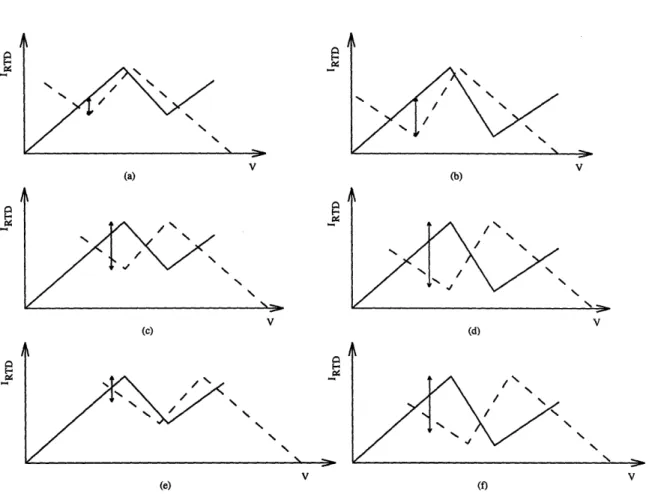
The static power of the SRAM cell is the product of the bias voltage of the RTD storage element and the static current of the individual states, either VLO or VHI. There is a finite range of bias voltages for which the diode chain will be bistable. Figure 2-3 shows schematically the different bias situations resulting in single, double, and triple operating points. For low bias voltages, Figure 2-3a, the operating point of the diode chain will occur where the pre-resonance rising legs of both diodes intersect. At a certain voltage, the valley of the load (driver) device will intersect the rising edge of the driver (load) device. For asymmetric diodes, i.e., where the load and driver have different I-V characteristics, the two events will not occur at the same voltage. Bistability occurs when either or both of these intersections occur, but the desired condition for a memory cells happens when both intersections exist, Figure 2-3b. For biases beyond the bistability range, the operating point will occur at the intersection of the post-resonance rising leg of both diodes, Figure 2-3c. For some diodes, three stable intersections can occur, Figure 2-3d. This is an undesirable situation because the middle voltage state is stable, and can be switched into. Figure 2-4 shows the measured voltage bistability range of a relaxed-buffer RTD (RBRTD) storage element.
The range of bistability is related to the peak and valley voltages and currents of the RTD. The peak and valley voltages and currents of the RTDs are Vp, Vv, Ip, and Iv, respectively and are shown in Figure 2-3c. (The peak and valley current densities of the RTD are Jp and Jv, respectively.) For bistable operation, the minimum bias voltage is twice the maximum of the peak voltages of the two RTDs in the storage element, Vp,ma. For a given peak-to-valley voltage ratio, a diode with a lower valley current will also extend this range because the valley of the load (driver) device will overlap the rising edge of the driver (load) device for a larger supply
2.2 Static Power of an RTD-EFET SRAM '7
VRTD
VLO
VHI VRTD
(a) (b) VP VV VRTD VRTD (c) (d)Figure 2-3: Load line characteristics as a function of VRTD: (a) VRTD below bistability range;
(b) VRTD in bistability range; (c) VRTD beyond bistability range; (d) VRTD resulting in tristable
situation. Stable operating points are marked with filled circles. Vp, Vv, Ip, and Iv are marked
in (c).
voltage. The static current of both VLO and VHI will increase with increasing bias voltage. For asymmetric diodes, the currents of these two states will be different. The dependence of the static current will be proportional to the post-resonance valley current. The lower the valley current of the devices, the lower the static power of the cell will be. In addition, a broad, low-current valley is desirable to accommodate variations in RTD peak and valley voltages without substantially varying the static power across an array of diodes.
2.2 Static Power of an RTD-EFET SRAM
0.5
S0.4
S0.3
S0.2
m 0.1
00
z
0.0
0.2
0.4
0.6
0.8
1.0
VRTD
(V)
Figure 2-4: Measured voltage bistability of an RBRTD storage element. The device areas are
25 pm
2and Vp,ma is 0.344 V.
2.3 Switching Current of an RTD-EFET SRAM
2.3 Switching Current of an RTD-EFET SRAM
Figure 2-5 shows the measured minimum required switching current, Iswitch,min, for an RTD storage element. This is the current that an EFET must supply to write a HI or LO to this storage element. For biases below 1.1 V, the RTD storage element is in a region of tristability. For completeness, a description of the minimum required current to switch the chain is included. However, this is not a preferred region of operation for the memory.
I
2
·. (45.0
40.0
35.0
30.0
25.0
20.0
1 a1.1.
.0
1.2
1.4
1.6
VRTD
(V)
1.8
Figure 2-5: Measured Iswitch,min requirements for a pseudomorphic RTD storage
device areas of 100 pm2 and a maximum peak current density of 9.09 kA/cm2
element with
For bias voltages Vp < VRTD < 2Vp, the memory element is in a region of tristability. In
this situation, shown in Figure 2-6a, there are 4 currents to consider. When switching from LO to HI, currents b and c set the minimum, and when switching from HI to LO, currents a and d set the minimum. For biases in this range, current must be added (subtracted) from the storage node such that the sum of the added (subtracted) current and the valley current of the load (driver) no longer intersects the pre-resonance rising leg of the driver (load), and the peak current of the driver (load) is less than the sum of the injected (subtracted) current and the pre-resonance rising leg of the load (driver). In the case of symmetric RTDs, Iswitch,min will occur at the bias where b = c and a = d. For asymmetric diodes, the minimum current will be
the maximum of the two. Because there is a stable middle storage node voltage for this bias
.
. I I
I I I I I I I-A-
I I I I I I I I I I I I I IL
L
2.4 Switching Speed of an RTD-EFET SRAM
VRTD VRTD
(a) TD (b)
Figure 2-6: Schematics showing Iswitch,min (a) in tristable region (b) in bistable region.
range, however, the Iswitch,min is not practical for a memory cell.
For biases VRTD > 2VP,max, Figure 2-6b, currents b and d establish the switching current
requirement. The maximum Iswitch,min needed, in magnitude, will be (Ip - Iv)max. To change
the state of the memory, the EFET must be able to supply this magnitude of current. For a given EFET, designing the memory to require lower switching current will result in a cell with higher static power. When switching the cell, the EFET is doing the initial charging of the storage node. For a given VRTD, the more current beyond Iswitch,min that the EFET can supply, the faster the switch will be.
VGs and VDs of the EFET will change during the write operations. Care must be taken that the EFET design accounts for the reduction in current. Specifically, the EFET must be large enough to supply at least Iswitch,min as long as there are two stable operating points for the storage element. (Another way to think of this, described in Section 2.4, is that the EFET must supply current as long as the storage node voltage is in a range where the RTDs cannot push the switch. For symmetric RTDs, this voltage will be VRTD/2.) To account for the reduction in current, the EFET will have to be "oversized."
2.4 Switching Speed of an RTD-EFET SRAM
Most of the investigations in the literature of tunnel-diode switching speed have focused on the use of diodes in logic circuits, initially using Esaki tunnel diodes and later RTDs. Many investigations specifically looked at the time necessary for a diode to switch from its peak to valley voltage and vice versa [21, 22, 23]. In all cases, the speed of the diode voltage switch was determined by the ability of the diode to charge its depletion capacitor. Likewise, the speed of the memory cell will be determined by the ability of the EFET and the RTDs to charge and discharge the storage node capacitance. The major differences are that the voltage switch
2.4 Switching Speed of an RTD-EFET SRAM
happens over a much greater voltage region than the previous investigations, the load is no longer a simple resistor, and the node capacitance includes that of an additional RTD and an EFET. This section focuses on the effects various RTD-EFET SRAM cell parameters have on the switching speed.
2.4.1
SRAM
Model Description
Figure 2-7 shows the evolution of the RTD SRAM model. Equations 2.1- 2.3 describe the dynamics of the memory cell:
dVRTD1 dVRTD2 dVRTD2
IRTD1 CRTD1 + IEFET(VGS, VGD) = IRTD2 + CRTD2 + Cs d(2.1)
dt dt dt
where IRTD is the current in an RTD and CRTD is the RTD capacitance. The capacitance of the
EFET source contact is Cs. Writing VRTD1 in terms of VRTD2 and combining terms gives
dVRTD1 dVRTD dVRTD2 dVRTD2(
dt - dt dt - dt
IRTD1 - IRTD2 + IEFET(VGS, VGD) = [CRTD1 + CRTD2 + CS] dVRTD2 (2.3)
The EFET source node capacitance can be combined with the capacitances of the two RTDs to form the storage node capacitance, Cnode. Recognizing that VRTD2 is the storage node voltage
yields
dVnode
IRTD1 - IRTD2 + IEFET(VGs, VGD) = Cnode d . (2.4) dt
To analytically solve for the storage node voltage as a function of time, Equation 2.5 is solved for the piecewise-linear regions of the switch and the switching times for each region are then summed to calculate the total switching time.
t = dt = Cnode dVnode (2.5)
J IRTD1 - IRTD2 + IEFET
For a complete listing of the analytical solutions to Equation 2.5 the reader is referred to Appendix A. Because the intent of this model is to focus on the role of the RTD in the memory, further assumptions are made:
* The RTDs used are symmetric with respect to voltage.
* Load and driver RTDs are identical. The pre-resonance conductance of the RTDs is G1
and the post-resonance conductance of the RTDs is G2.
* The RTD negative differential resistance (NDR) region is modeled as a finite, linear resistor with conductance GN.
2.4 Switching Speed of an RTD-EFET SRAM
* To simulate the EFET turning off during the switch, the EFET current is modeled as
constant for Vnode < VRTD - Vp. This will only simulate the slowest of the write actions:
WRITE HI when the EFET cuts off. The current is actually on longer than the minimum
time (tmin occurs when Vnode = VRTD/2), but is assumed to be zero for t > tmin for simplicity
and to account for noise margins for the switch.
* VRTD > 2Vp to insure that there is no stable middle voltage node.
VRTD SELECT C node RTD T1- 11<1 2 T2 - 1 <1 2 T3 - I 1 ' I 2 T4 - 11>I2 T5 I- 1>I2 RTD 1 pushing RTD 1 & RTD2 pushing RTD 2 pushing VLO VHI
Figure 2-7: Evolution of the RTD-EFET SRAM switching model. The circuit elements are reduced and combined to form a simplified circuit architecture. Current and voltage continuity at the storage node are used to describe the action of the cell. The transition from VLO to VHI is broken into 5 regions. Case 2, VRTD > 2Vp and VRTD < Vp+ VV, is shown in this figure.
Four different bias cases are considered: * Case 1: VRTD = 2Vp
* Case 2: VRTD > 2Vp and VRTD < Vp+ VV
* Case 3: VRTD > 2Vp, VRTD > Vp+ Vv and VRTD < 2Vv 2
2.4 Switching Speed of an RTD-EFET SRAM
* Case 4: VRTD > 2Vp and VRTD > 2Vv
For Cases 2 to 4, there are 5 distinct regions in the voltage switch. For Case 1, there are four distinct regions.
Region 1: Current is being supplied to the storage node via the EFET and the load RTD. Without the added EFET current, the load RTD cannot charge the storage node. For all cases, as the voltage at the storage node rises, the current injected into the storage node decreases because the load RTD is pushed closer to its valley. This is a standard RC charging situation where rl = Cnode/(G1 + G2). As the storage node rises in voltage, it becomes harder to charge
the storage node.
Region 2: Current is being supplied to the storage node via the EFET and the load RTD. Without the added EFET current, the load RTD cannot source the current to charge the storage node. For Cases 1 and 2, as the voltage at the storage node rises, the current injected into the storage node increases because the load RTD is pushed through its NDR region towards its peak. For these cases, 72 = Cnode/(G+1 GN), and the load RTD is pushing the storage node higher in voltage. For Cases 3 and 4, as the voltage at the storage node increases, the current demand of the driver RTD decreases because it is being pushed through its NDR region. Simultaneously, the current supplied by the load RTD is decreasing as it is pushed towards its valley. In these cases, 72 = Cnode/(G2 + GN), and the voltage at the storage node is pushed higher by the driver RTD.
Region 3: This region is specific to Cases 2 to 4. Current is being supplied to the storage node via the EFET and the load RTD. When Vnode < VRTD/2, the load RTD cannot source the current to charge the storage node without the added EFET current. However for Vnode > VRTD/ 2, the
load RTD sources more current than the driver RTD demands. Here, 73 = Cnode/2GN. Both RTDs are in their respective NDR regions and both push the storage node higher in voltage. As the storage node voltage rises, the load RTD supplies, and the driver RTD demands, less current. This allows more charge to build up on the storage node capacitor, forcing the storage node even higher.
Region 4: The model assumes that the EFET has been turned off in this region. For Cases 1 and 2, the load RTD sources more current than the driver RTD demands. The driver RTD is in its NDR region, and as the storage node voltage increases, the driver RTD will demand progressively less current. Though the load RTD will supply decreasing amounts of current with the increasing storage node voltage, its rate of decline is much less than the driver RTD demand decline, and thus "surplus" current will be available to charge the storage node. For these cases, 74 = Cnode/(G1 + GN), and the driver RTD is pushing the storage node. For Cases 3 and 4, the load RTD is supplying increasing amounts of current as it is pushed through its NDR region and the driver RTD is demanding increasing amounts of current as it is pushed beyond it valley. The rate of increase in the load current supply will exceed the driver demand increase, and once again, "surplus" current will be available to charge the storage node. For
2.4 Switching Speed of an RTD-EFET SRAM
Region 5: For all cases, in this region the load RTD current supply is decreasing and the driver RTD current demand is increasing, but the load supply is always greater than or equal to the driver demand. Because the load is supplying more current than the driver demands, the storage node will rise, but neither diode is driving the storage node because as the the voltage rises, less current is available to charge the storage node capacitance. In this region,
r5 = Cnode/(G1 + G2), and it once again looks like a standard RC charging problem.
For the following discussions, the RTD and EFET are based on devices that experimentally have been fabricated and integrated. This "reference" RTD has a peak voltage of 0.2888 V, a valley voltage of 0.4195 V, a peak current density of 1.01 kA/cm2, and a peak-to-valley current ratio, PVCR, of 2.3:1. The diode area is 25 Mm2. Using a parallel plate assumption, the depletion capacitance of the RTD is calculated to be 10 fF. The EFET used in the integration was 10 x 1.2 ~m. Its source node capacitance, 20 fF, was calculated using capacitance per unit area numbers supplied by Vitesse as part of their HSPICE models. Interconnect capacitances are included by increasing the source node capacitance. Series resistances in the RTDs are not included. This particular RTD-EFET combination was chosen to correspond to an experimental demonstration present later in the thesis. However, the results are general in nature, and the effects of changes in RTD and EFET size will be discussed for each analysis.
2.4.2
Effects of PVCR
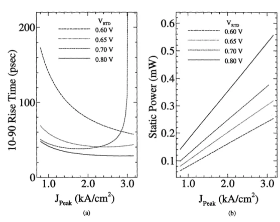
To assess the effect of changing the PVCR of the RTDs on the switching time, the valley current of the RTD was decreased and the peak current of the RTD was held constant. Figure 2-8 shows the effect of changing the PVCR on the 10-90 rise time to write a HI and on the cell static power, both as a function of bias voltage. In this calculation, interconnect capacitances are ignored. G1 and G2 are obtained from the reference diode, and are held constant as Iv, and
hence GN are changed. For these calculations the switching current was 0.4 mA.
For a given VRTD, the variation of PVCR has different effects. Consider first the case VRTD= 0.6 V. As the PVCR increases the amount of current the load RTD contributes (the dotted line in Figure 2-9a and b) in the initial part of the switch decreases. Therefore, the time spent in regions T1 and T2 of the switch increases. However, since the EFET is the
dominant current source in these regions of the switch, the effects of the PVCR changes are not significant. For situations where IGNI ,G 1 and IRTD1 ; IRTD2, the driver RTD is sinking
most of the current available to charge the node. As the PVCR is increased, the corresponding reduction in Iv increases IGNI, and thus the RTDs drive the switch harder. In the latter half of the switch, increased PVCR leads a decrease in the time spent in regions T4 and Ts. The
reduction in switching time is due to an increase in the difference between supply and demand current. The extra charge is dumped on the capacitor. The reduction in time spent in regions T4 and T5 outweighs the increase in regions T1 and T2, and thus the overall switching time is
reduced.
32 2.4 Switching Speed of an RTD-EFET SRAM
200
100
0 d/ I\0.2
oS
5
15
25
5
15
25
PVCR
PVCR
(a) (b)Figure 2-8: Effects of changing RTD PVCR on (a) 10-90 switching time and (b) cell static power as a function of VRTD with constant current density.
substantial. This can been seen in the time constants of the switch. For regions T2 and T4,
7 = Cnode/(G1 + GN). For IGNI
>
G1, T = Cnode/GN. The minimum required switching currentthat must be supplied by the EFET will increase with PVCR, but for this bias case the required current is still far below that being supplied by the EFET. Thus, the switching time continues to slowly decrease with increased PVCR.
For VRTD = 0.7 V, the ratio of supply/demand current decreases in regions T1 and T2 and
increases in regions T4 and T5. However, this bias has the highestlswitch,min of those considered.
As the PVCR increases, Iswitch,min also increases. The "surplus" current left to charge the node decreases, and thus the speed of the overall switch decreases. Once again, for IGNI
>
G1,7 = Cnode/GN. In this case the effects of the increase in minimum switching current required outweigh the effects of a larger IGNI, and the speed slowly continues to decrease. For VRTD = 0.8
V, the dependence on PVCR is the same as that for VRTD = 0.7 V. VRTD = 0.7 V has the greatest
surplus current, and therefore is the fastest bias case.
Across a memory array, there will be variations in RTD Jp, Jv, Vp, and Vv. This set of
parameters explicitly accounts for the current variations. Variations in RTD voltages can be represented by assuming a spread of VRTD. It is desirable to design in tolerance for these varia-tions. Of the two SRAM figures of merit considered here, it is preferable to have the variations
S'VRTD -0.60 V 0.65 V ... --...--- . . 0.70 V 0.80 V - -VRTD --- 0.60 V ... 0 .6 5 V ,0.70V 0.80V . .0 -,--- -I -I , • • a , II I ) • , ,I ,
2.4 Switching Speed of an RTD-EFET SRAM 33 0 N N / N N / N N N (a) V
&J
0~ 0 \ \I (c) V 0l 0• \-V V (e) (f)Figure 2-9: Storage element load lines as a function of VRTD and PVCR: (a) VRTD = 0.6 V, low
PVCR; (b) VRTD = 0.6 V, high PVCR; (c) VRTD = 0.7 V, low PVCR; (d) VRTD = 0.7 V, high PVCR;
(e) VRTD = 0.8 V, low PVCR; (f) VRTD = 0.8 V, high PVCR. In each situation, the minimum
required switching current is indicated with an arrow.
in RTD characteristics manifest themselves as variations in the static power dissipated in a cell. In addition, one would like to maintain a low static power. Both of these constraints can be satisfied by designing RTDs with high PVCR. High is a relative term. Exactly how high the PVCR should be will be determined by the EFET. The PVCR cannot result in a Iswitch,min that is beyond the capacity of the EFET. In this example, because this EFET can supply enough current to switch this RTD storage element regardless of RTD PVCR, a design with a very high PVCR, 25:1, should be used to minimize static power. In addition, the RTDs should be designed such that the Vp+ VV VRTD, where VRTD is the supply bias of the storage element.
For a given EFET size, reduction in RTD area will decrease the storage node capacitance and increase the surplus current supplied by the EFET to charge to storage node. These factors will lead to an increase in switching speed. Reduction of EFET size for a given RTD size will decrease the storage node capacitance. However, the resulting gains in speed will be offset by the reduction in the current sourcing capability of the EFET, which will reduce the speed.
a
1
(a)
w
2.4 Switching Speed of an RTD-EFET SRAM
2.4.3 Effects of Current Density
2.0
JPeak (kA/cm
2)
(a)3.0
0 0/ U,1.0
2.0
JPeak (kA/cm
2)
(b)Figure 2-10: Effects of RTD current density on (a) 10-90 switching time and (b) cell static power as a function of VRTD and with constant PVCR.
To assess the effect of changing the current density of the RTD, the PVCR was held constant (at the reference RTD PVCR) while the peak and valley currents were changed. The perfor-mance of the cell was again evaluated at a number of RTD bias voltages. In this study, G1, GN,
and G2 all are changing.
Figures 2-10 and 2-11 show the performance of the cell and the load line characteristics of the memory element, respectively. The performance effects of varying the current density are similar to those of varying the PVCR. For VRTD = 0.6 V, as current density increases
the difference between the demand and supply currents increases. For regions T1 and T2,
there is an increasing deficit of current which must be supplied by the EFET. Because the EFET is supplying well beyond the Iswitch,min, the effects of the reduced supply current are not substantial. In regions T4 and T5 there is an increase in the surplus current available to charge
the storage node, and the time spent in these regions of the switch is reduced. This effect is stronger than the time increase in regions T1 and T2, and thus the overall switching time will
be reduced as the current density of the RTDs is increased.
For VRTD = 0.7 V the same increase in T1 and T2 and decrease in T4 and T5 occur. However,
for this bias voltage, as the current density increases the minimum switching current increases
200
0 rA 0 0ON
6
r--100
0U
1.
3.0
2.4 Switching Speed of an RTD-EFET SRAM
to values close to that supplied by the EFET. For higher current densities, there is less surplus current to charge the storage node. This effect is the dominant one and therefore there is an increase in the overall switching time as the RTD current density increases.
Two factors contribute to the overall speed of VRTD = 0.8 V: very little switching current is necessary for all current densities, and the majority of the switch occurs over regions where one of the RTDs is pushing the switch forward. The same general trends apply with respect to increasing current density, and thus the speed of the switch increases for higher current density devices.
As expected, the static power dissipated in a cell increases with increasing bias voltage. In addition, the static power increases with increasing current density. This is primarily due to the increase in valley current density. Switching speeds are overall faster than for the previous
N N / N N N / -/ N N N V (a) N 1 /N / N N N / (b) // I/ / \ \ // \ /
Figure 2-11: Storage element load lines as a function of VRTD and current density (CD): (a)
VRTD = 0.6 V, low CD; (b) VRTD = 0.6 V, high CD; (c) VRTD = 0.7 V, low CD; (d) VRTD = 0.7 V,
high CD; (e) VRTD = 0.8 V, low CD; (f) VRTD = 0.8 V, high CD. In each situation, the minimum required switching current is indicated with an arrow.
2.4 Switching Speed of an RTD-EFET SRAM
case because more current is available to charge the storage node.
To design for robustness, once again, the RTD current density should be such that changes in current density and supply voltage have a minimal effect on the 10-90 rise time of the cell. The RTDs should be designed such that the bias voltage is greater than Vp+ Vv to accommodate variations in current density. In addition, for this EFET, current densities in the 1-2 kA/cm2 range are preferable.
The general area trade-offs are the same as for the previous analysis. Reductions in RTD area for a given EFET will increase the speed of the switch. Reduction in EFET size for a given RTD area will lead to a reduction in the cell switching speed.
2.4.4 Combined Effects of PVCR and Current Density
1.U
Z.U
0
.U
JPeak(kA/cm
2)
~0.2
0.1
1.0
2.0
JPeak
(kA/cm
2)
Figure 2-12: Effects of RTD peak current density and associated PVCR on (a) 10-90 switching time and (b) cell static power as a function of VRTD for constant Jv.
The previous two analyses demonstrate the low power advantages of high PVCR and the speed advantages of higher current density. By designing RTDs with thin, wide-bandgap barriers, it may be possible to combine these advantages. Thus, a study of the combined effects of PVCR and current density was performed. The valley current of the RTD was held constant and the peak current of the RTD was increased. As the peak current density increases, there is an associated increase in the PVCR of the RTD. In this study, G1 and GN change, but G2 is
20
1 0 0 !\ 0.65 V ... 0.70 V 0.80 V S I L . . . -.--- I- L3.0
~ ' ' ' ' ' ' ' ' ' ' ' ' -ruýý!
rrvaK2.4 Switching Speed of an RTD-EFET SRAM
held constant.
Figure 2-12 shows the performance as the RTD peak current density and associated PVCR are increased. For all bias voltages, the trends follow those established in the previous two analyses. At low current densities, where the EFET is providing more than enough switching current, the increase in surplus current with increased VRTD in regions T4 and T5 increases the
speed of the switch. For high current densities, the speed is limited by the lack of switching current being supplied by the EFET.
Combining increased current density and PVCR actually improves the tolerance of the cell. For Jp = 1.6 kA/cm2, the cell can handle a 0.15 V variation in VRTD without changing the 10-90 rise time of the cell. For Jp = 1-2 kA/cm2 and PVCR = 2.3-4.5, the EFET is still supplying enough switching current. In this range, the speed of the cell is somewhat slower than the case of varying current density only. However, for higher VRTD there is approximately a 1/3 reduction in power. For this same current range, increasing the PVCR by reducing the valley
current will produce lower static current. Manipulation of the valley current substantially reduces the tolerance of the cell to RTD parameter variations.
0 E 0, 0
1.U
2.0
JSp
(kA/cm
2)
Figure 2-13: SRAM 10-90 switching time as a function of peak current density (and associated PVCR) with node capacitance as a parameter and VRTD = 0.7 V.
Figure 2-13 shows the effect of changing the node capacitance for VRTD = 0.7 V. As