HAL Id: hal-01473612
https://hal.archives-ouvertes.fr/hal-01473612
Submitted on 2 Jul 2020HAL is a multi-disciplinary open access archive for the deposit and dissemination of sci-entific research documents, whether they are pub-lished or not. The documents may come from teaching and research institutions in France or abroad, or from public or private research centers.
L’archive ouverte pluridisciplinaire HAL, est destinée au dépôt et à la diffusion de documents scientifiques de niveau recherche, publiés ou non, émanant des établissements d’enseignement et de recherche français ou étrangers, des laboratoires publics ou privés.
Phototransport in colloidal nanoplatelets array
Emmanuel Lhuillier, Jean-Francois Dayen, Daniel O. Thomas, Adrien Robin,
Sandrine Ithurria, Herve Aubin, Benoit Dubertret
To cite this version:
Emmanuel Lhuillier, Jean-Francois Dayen, Daniel O. Thomas, Adrien Robin, Sandrine Ithurria, et al.. Phototransport in colloidal nanoplatelets array. physica status solidi (c), Wiley, 2016, 13 (7-9), pp.526 - 529. �10.1002/pssc.201510165�. �hal-01473612�
Phototransport in colloidal Nanoplatelets Array
Emmanuel Lhuillier1,2*, Jean-Francois Dayen3, Daniel O. Thomas4, Adrien Robin,1,4 Sandrine Ithurria4,
Herve Aubin4, Benoit Dubertret4 1Nexdot, 10 rue Vauquelin, Paris, France
2CNRS, UMR 7588, Institut des Nano-Sciences de Paris (INSP), 4 place Jussieu, 75005 Paris, France
3Université de Strasbourg, IPCMS-CMRS UMR 7504, 23 Rue du Loess, 67034 Strasbourg, France
4 Laboratoire de Physique et d’Etude des Matériaux, ESPCI-ParisTech, PSL Research University,
Sorbonne Université UPMC Univ Paris 06, CNRS, 10 rue Vauquelin 75005 Paris, France. (*) Contact: [email protected]
Abstract: Colloidal nanocrystals are promising materials for achieving low cost optoelectronic devices. In this paper, we focus on the transport and photo transport properties of 2D nanoplatelet thin films and their use for photodetection. We present evidence that improved performances relies on good trap passivation as well as overcoming the inherent large exciton binding energy of the 2D NPL. This can be achieved using a phototransistor configuration with transport at the single particle scale. Keywords: semiconductor nanoparticles, quantum dot, nanoplatelets, photodetection, electrolyte gating, noise.
1. INTRODUCTION
Colloidal nanocrystals have raised great hope towards achieving low cost optoelectronic devices,1
however this goal requires fine control over both optical and transport properties of nanocrystal arrays. Over the past two decades, great progress has been obtained on the synthetic procedure of colloidal quantum dots which can now be achieved for a large range of materials with band gap spanning from UV to mid IR2,3. Improved synthetic procedures now allow achieving nano-objects with
controlled dimensionality as well as those based on complex core shell heterostructures.
Among these colloidal materials, 2D nanoplatelets4,5 (NPL) based on cadmium chalcogenides6 offer
particularly interesting structural and optical properties. Thanks to their large lateral extension above the Bohr radius, the quantum confinement only occurs in one direction. Moreover the thickness is perfectly controlled at the atomic scale (i.e. there is no roughness). This results in extremely narrow optical features (Figure 1b) due to the absence of inhomogeneous broadening. Moreover, the 2D aspect of the nanoparticles leads to a high exciton binding energy7,8 (250meV) and a fast
photoluminescence lifetime. While the spectroscopic properties have attracted huge interest in particular for stimulated emission, the integration of NPL9 into conductive devices remains far less
investigated10,11. Nevertheless, NPL look promising because their sharp optical features can be used to
develop narrow emission electroluminescence devices12 or photodetectors with finely controlled
cut-off wavelengths. In this article, we review some of the recent results obtained by our group in the integration of NPL for visible photodetection.
2. METHODS CdSe core
In a 100ml three neck flask, 240mg of cadmium myristate, 25mg of selenium powder and 30mL of octadecene are mixed and degassed under vacuum at 80°C for 30min. The temperature of the flask is then set at 240°C. Once the content of the flask reached 190°C, 160mg of cadmium acetate are quickly added to the flask while removing the septum. The solution is then further heated at 240°C for 12min before 1mL of oleic acid is injected to quench the solution. The flask is cooled and its content precipitated by addition of ethanol. After centrifugation the formed pellet is redispersed in fresh hexane.
CdSe/CdS core shell synthesis
The growth of a CdS shell is performed at room temperature using the c-ALD procedure13. The CdSe
NPL cores are successively exposed to cadmium and sulfide precursor and the excess precursor is removed by beaning at each step. A total of 3.5 layers of CdS is grown.
Ligand exchange
NPL originally dispersed in hexane are mixed with a mixture of sodium sulfide in N-methyl formamide (NMFA). After strong sonication, the particles get phase transferred. The polar phase is then cleaned three times by addition of hexane. The clear top phase is discarded each time. Ethanol is added to precipitate the particle. The formed pellet is eventually dispersed in pure NMFA.
Electrode fabrication
A Si/SiO2 substrate is cleaned by sonication in acetone for 5min. The wafer is then rinsed using
isopropanol. Once dried, the wafer is further cleaned using O2 plasma for 5min. AZ5214E lithography
resist is then spin-coated on the wafer and the solvent dried by cooking the wafer on a hot plate at 110°C for 90s. The wafer is then illuminated through a shadow mask for 2s, before being cooked on a hot plate at 125°C for 2min. A flood UV exposure of the wafer is performed for 40s. The patterns are then developed in AZ326 for 32s. Then 3nm Cr and 40nm gold are thermally evaporated. Finally the wafer is dipped overnight in an acetone bath and eventually rinsed with isopropanol before being dried.
Nanotrenches are prepared using two steps of the previously described14 procedure. The first step
defines the source while the second evaporation defining the drain is performed under a 60° tilt. Electrolyte preparation
In an air free glove box, 50mg of LiClO4 are mixed in 230mg of polyethylene glycol for two hours on a
hot plate at 170°C. Thin film preparation
In an air free glove box, the nanoparticles are drop-casted onto the electrodes on a hot plate at 100°C. Once the film is dried, the melted electrolyte is brushed directly on the film and a metallic grid is deposited on the top of the electrolyte to be used as top gate.
3. RESULTS AND DISCUSSION 3.1. Photoconductive properties
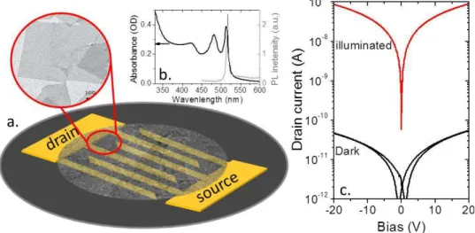
As a first step in investigating the photoconductive properties of NPL, we focus on the transport in a NPL thin film connected with µm spaced interdigitated electrodes (Figure 1a). While the conductance of the film is very low under dark condition, we observe a significant current modulation under
illumination,15,16 whose photon energy is above the band gap, see Figure 1c. This photocurrent has a
fast time response16 (f
3db >100kHz) and a linear dependence with the photon flux. However, the overall
photoresponse is weak (few µA.W-1). In such devices, the transport occurs through a hopping process
as the nanoparticle size remains far smaller than the electrode spacing. At each hopping step, the photocarrier has to overcome a tunnel barrier and may get trapped on surface defects. Ligand exchange17 from long alkane chain to atomically short (S2-) has been conducted to improve the overall
mobility, however it is insufficient to achieve a large photoresponse.
Figure 1 a. scheme of a photoconductive device based on Nanoplatelets thin film connected to interdigitated electrodes. The inset is a Transmission Electron Microscopy image of CdTe NPL. b absorption and photoluminescence spectra of CdSe NPL. C current as a function of the applied bias for a CdSe NPL thin film under dark condition and under illumination (50mW of a 405nm laser).
3.2. From photoconductor to phototransistor
In order to improve the ability of this material to convert light into current, we propose to build a phototransistor. Gating of colloidal nanocrystals can be obtained through a conventional solid state approach using a thin dielectric. However, with such gating the carrier density modulation remains low (<1013cm-2), which is generally less than 1 carrier per dot. Larger carrier density can be obtained while
switching to electrolyte gating. In this case, the sheet capacitance is indeed no longer given by the ratio of the dielectric constant by the dielectric thickness but rather by the ratio of the dielectric constant by the ion size. The latter can be as small as 100pm in the case of Li+, which allows carrier density above
1014cm-2. Liquid electrolytes are generally used to gate nanocrystals film, but this strategy remains
poorly integrable for real optoelectronic devices since electrochemical cells are bulky and leaky. We develop an ion gel approach for NPL thin film gating18 which combines several advantages: (i) gating is
solid and compact, (ii) the obtained devices are air operable and (iii) the method is also able to gate thick films (µm). In practice, LiClO4 dissolved in a polyethylene glycol matrix is melted and deposited
solvent free on the nanoparticle film. This approach leads to an electrolytically gated transistor with exceptional performance19. The on/off ratio reaches nearly 9 decades, while the subthreshold slope
can be as small as 80mV/decade, see Figure 2a. The driving gate bias remains moreover limited to a few volts. As a consequence, we can take advantage of this very sharp change of the current with the carrier density to build a phototransistor. By operating the transistor close to its turn on threshold, we bring the system in a regime where the current dependence with the carrier density is no longer linear but rather exponential. Thus, by shining light on the sample, the excess photocarriers are expected to
bring a dramatic current modulation. This was indeed experimentally observed16 : The typical
photocurrent enhancement under gate bias ranges from 100 to 1000. As a positive gate bias is applied, cations from the electrolyte start penetrating the nanoparticles film. As a consequence, the electrodes inject electrons in the NPL. Since NPL are intrinsically undoped, the Fermi level is expected to be close to the middle of the band gap. As electrons get injected, the Fermi level moves toward the conduction band and start filling the unpassivated trap states likely introduced by the c-ALD growth process. The filling of these trap states increases the photocarriers lifetime in the conduction band, since they can no longer be trapped after their photogeneration. This leads to an increased overall gain and explains the improved photoresponse16. However, this increased gain comes at the price of reduced bandwidth
which drops at the same ratio as the gain increases.
Figure 2 Drain current and photoresponse as a function of gate bias for a CdSe/CdS NPL thin film gated with an ion gel electrolyte. The inset is a scheme of the device. For b and c the device is made of CdSe/CdS NPL film gated with electrolyte in parallel with a non gated HgTe nanocristal film. b (resp. c) represents the current as a function of time during an illumination pulse by a near IR LED (980nm) followed by a blue Laser pulse (405nm) under 0V gate bias (resp. 1.1V gate bias).
This gating approach can also be used to build a bicolor nanocrystal based detector. Such a device is of particular interest once operated in the infrared. Indeed, bicolor detection not only provides thermal contrast but can also discriminate objects with different emissivity. To do so we combine a CdSe/CdS NPL phototransistor with a 630nm cut-off wavelength in parallel with a photoconductive sample made from HgTe colloidal quantum dots (λcut-off=2.1µm). In absence of gate bias, the narrow band gap
material dominates the transport because of the larger number of thermally activated carriers. Thus, only the photoresponse of the HgTe thin film is observed. As a result, the system is responsive both in the visible and near IR, see Figure 2b. Once the CdSe/CdS NPL film is gated, its conductance rises and can even overcome the conduction of the HgTe film. In this situation, the infrared photoresponse is washed out and only the signal originating from visible illumination is measured, see Figure 2b.
3.3. Photoconduction with optimized transport at the nanoscale
While electrolyte gating is an efficient strategy to get rid of surface traps, it does not address the large exciton binding energy which is inherent to 2D systems7,8. With an exciton binding energy significantly
larger than the thermal energy or the electric field drop per particle, it is very unlikely that the photogenerated electron-hole pairs get efficiently dissociated. To overcome this issue, a larger electric field needs to be applied, which can be obtained by shrinking the device size. Switching to smaller devices is also very appealing in order to get rid of µm scale morphology defects inside the NPL film. We use a simple method based on a two steps optical lithography to design nanotrenches with short electrode spacing (20 to 100nm) but large aspect ratio 14. A picture of the device functionalized with
CdSe/CdS NPL is given on Figure 3a.
Figure 3 a is an SEM image of a nanotrench decorated with CdSe/CdS NPL. b. Photoresponse as a function of incident light power for a nanotrench based device. A fit with a power law has been added.
In such nanotrench devices, the photoresponse is dramatically boosted20 compared to the same
material operated in the hopping regime, and responsivity as large as 1kA.W-1 has been demonstrated.
This value is the record value obtained for CdSe nanomaterial based devices. It is worth noting that similar responsivity have already been reported in PbS nanocrystals film21, in which the large dielectric
constant of the material allows the photocarriers to behave almost as free carriers. In our case, the large applied electric field fully compensates the binding energy. In addition to this increased charge dissociation, the 8 decades boost of the photoresponse compared to µm scale devices is also the result of a large gain, corresponding to 3000 generated electrons per absorbed photon. 22 Small electrode
spacing indeed results in short transit time and thus large gain. The last element which contributes to the improved performance is evidenced by the root square power dependence of the photoresponse (IαP-1/2, see Figure 3b) which is consistent with current limited by electron-hole pair recombination23
rather than by trapping. Contrary to hopping transport where the photocarriers will very likely experience trap states regardless of the path they take, in nanotrench devices the paths limited by trap states are simply ineffective and do not participate in the transport. In this geometry, the transport is actually limited by the charge carrier injection at the contact and careful contact engineering will be required to obtain even higher performance20.
4. CONCLUSION AND PERSPECTIVES
We demonstrate that nanoplatelets are a promising material to achieve low cost photodetectors as long as we can take care of their specific properties such as their large exciton binding energy. Further improvements are needed to increase the optical absorption in nanotrench devices and to reduce the Schottky barrier at the contacts. Another aspect needing to be addressed is the electrical noise which remains limited by the 1/f contribution24 in disordered nanocrystals arrays.
5. ACKNOWLEDGEMENTS
The authors thank Xiang Zhen Xu for her help with TEM imaging. We thank Agence National de la Recherche for funding through grants SNAP and H2DH. This work has been supported by the Region Ile-de-France in the framework of DIM Nano-K.
6. REFERENCES
1 D. Talapin, J.S. Lee, M. Kovalenko, E. Shevchenko , Chem. Rev. 110, 389 (2010). 2 E. Lhuillier, S. Keuleyan, H Liu and P. Guyot-Sionnest, Chem. Mat 25, 1272 (2013). 3 S. Keuleyan, E. Lhuillier, V. Brajuskovic and P. Guyot-Sionnest, Nat Photon 5, 489 (2011). 4 S. Ithurria, B. Dubertret, J. Am. Chem. Soc. 130, 16504 (2008).
5 C.Schliehe, B. H. Juarez, M. Pelletier, S. Jander, D. Greshnykh, M. Nagel, A. Meyer, S. Forster, A. Kornowski, C.
Klinke, H. Weller, Science 329, 550 (2010).
6 S. Ithurria, M.D. Tessier, B. Mahler, R. P. S. M.Lobo, B. Dubertret, Al. L. Efros, Nat. Mater. 10, 936 (2011) 7 R. Benchamekh, N.A. Gippius J. Even, M.O. Nestoklon, J-M. Jancu, S. Ithurria, B. Dubertret, Al. L. Efros, P. Voisin,
Phys. Rev. B 89, 035307 (2014).
8 A.W. chtstein, A. Schliwa, A. Prudnikau, M. Hardzei, M. V. Artemyev, C. Thomsen, U. Woggon, Nano Lett. 12,
3151 (2012)
9 E. Lhuillier, S. Pedetti, S. Ithurria, B. Nadal, H. Heuclin, B. Dubertret, Acc. Chem. Res. 22, 48 (2015). 10 S. Dogan, T. Bielewicz, Y. Cai, C. Klinke, Appl. Phys. Lett. 101, 073102(2012).
11 T. Bielewicz, S. Dogan, C. Klinke, Small 11, 826 (2015).
12 Z.Y.Chen, B. Nadal, B. Mahler, H. Aubin, B. Dubertret, Adv. Funct. Mater. 24, 295 (2014). 13 S. Ithurria, D.V. Talapin, J. Am. Chem. Soc. 134, 18585 (2012).
14 J.F. Dayen, V. Faramarzi, M. Pauly, N.T.Kemp, M. Barbero, B.P. Pichon, H. Majjad, S. Begin-Colin, B. Doudin,
Nanotechnology 21, 335303 (2010)
15 S. Pedetti, B. Nadal, E. Lhuillier, B. Mahler, C. Bouet, B. Abécassis, X. Xu, B. Dubertret, Chem. Mat 25, 2455
(2013).
16 E. Lhuillier, A. Robin, S. Ithurria, H. Aubin, B. Dubertret, Nano Lett. 14, 2715(2014).
17 A. Nag, M.V. Kovalenko, J.S; Lee, W. Liu, N. Spokoyny, D.V. Talapin, J Am Chem Soc 133, 10612 (2011). 18 E. Lhuillier, S. Ithurria, A. Descamps-Mandine, T. Douillard, R. Castaing, X.Z. Xu, P-L. Taberna, P. Simon, H.
Aubin, B. Dubertret, J Phys Chem C 119, 21795 (2015).
19 E. Lhuillier, S. Pedetti, S. Ithurria, H. Heuclin, B. Nadal, A. Robin, G. Patriarche, N. Lequeux and B. Dubertret,
ACS Nano 8, 3813(2014).
20 E. Lhuillier, J.F. Dayen, D. O. Thomas, A. Robin, B. Doudin, B. Dubertret, Nano Lett 15, 1736 (2015).
21 G. Konstantatos, I. Howard, A. Fischer, S. Hoogland, J. Clifford, E. Klem, L. Levina, E.H. Sargent, Nature 442, 180
(2006).
22 Prins F., Buscema M., Seldenthuis J. S., Etaki S., Buchs G., Barkelid M., Zwiller V., Gao Y., Houtepen A. J.,
Siebbeles L. D. A., van der Zant H. S. J., Nano Lett. 12, 5740 (2012).
23 L. J. Willis, J.A. Faireld, T. Dadosh, M.D. Fischbein, M. Drndic, Nano Lett. 9, 4191 (2009). 24 H. Liu, E. Lhuillier, P. Guyot-Sionnest, J. Appl. Phys. 115, 154309 (2014).