Chemical Vapor Deposition of Functionalized
Isobenzofuran Polymers
by
Ylva Kristina Olsson
Civilingenj6r i Kemiteknik och Kemi
Kungliga Tekniska Higskolan, 2004
Submitted to the Department of Materials Science and Engineering in Partial
Fulfillment of the Requirements for the Degree of
Master of Science in Materials Science and Engineering
at the
Massachusetts Institute of Technology
FEBRUARY 2007
@ 2007 Massachusetts Institute of Technology 2007. All rights reserved.
lrjI:aUIt• LI " 1ULUI e.
Department of laterials Science and Engineering
January 22, 2007
C ertified by:...
,.1v..•...
-
...-...
Klavs F. Jensen
Professor of Materials Science and Engineering and
Lammot du Pont Professor of Chemical Engineering
Thesis Supervisor
Accepted
by: ...
...
...
..
... ... ...
....-Samuel M. Allen
PC)W' Prnfe.qnr nf Phvdqi ql MPetllhirov
Chair, Departmental Committee on Graduate Students
ARCHIVES
FEB
T n 2007
LIBRARIES
rr .1
CI~~L~Cl~'lrP ~t I\~~t~~Y·
Chemical Vapor Deposition of Functionalized
Isobenzofuran Polymers
by
Ylva Kristina Olsson
Submitted to the Department of Materials Science and Engineering On January 22, 2007, in partial fulfillment of the
Requirements for the Degree of Master of Science
Abstract
This thesis develops a platform for deposition of polymer thin films that can be further tailored by chemical surface modification. First, we explore chemical vapor deposition of functionalized isobenzofuran films using two different functional groups: pentafluorophenolate ester and alkyne. Both functional groups can be further modified using either ester substitution or click chemistry, respectively. The resulting thinfilms are characterized extensively using nuclear magnetic resonance (NMR), Raman spectoscopy, and X-ray photoelectron spectroscopy (XPS). We show that the functional groups remain on the surface post deposition for both films at cracking temperature not exceeding 6000C. However, gel permeation chromatography(GPC) measurements of the pentafluorophenolate ester films show only marginal polymerization. On the other hand, the alkyne films appear crosslinked and showed defect formation. Films deposited at ambient temperature show formation of a large number of microdefects. Increasing the deposition temperature, in addition to increasing the growth rate, also leads to formation of films with two distinct domains: one smooth domain with no microdefects and another filled with defects. Analogous to the deposition of unmodified isobenzofuran films, the films with alkyne moiety have a high refractive index and are transparent in the visible and near IR range. Second, we explore coating of poly(dimethyl siloxane) (PDMS) microfluidic devices with poly(glycidyl methacrylate) (PGMA) thin films using initiated hot filament chemical vapor deposition. We demonstrate a use of a new ultra violet (UV) initiated bonding method that allows PGMA coated PDMS devices to be sealed to PGMA coated glass, while maintaining the integrity of the majority of surface functional groups. This approach allowed us to further functionalize the channel walls with hexamethylene diamine (HMDA) and poly(ethylene glycol) (PEG)-bis(amine) to make a lasting hydrophilic surface. Bonding of devices proved to be stable up to 2 bar.
Thesis Supervisor: Klavs F. Jensen
Title: Professor of Materials Science and Engineering and Lammot du Pont Professor of Chemical Engineering
Acknowledgements
Professor Klavs Jensen, for the belief in my chemistry and polymer knowledge, and my capabilities. For excellent guiding and for showing a genuine interest in my future career. Thank you.
Dr. Jamil El-Ali, without whom this thesis would never have been finished. Also many thanks for many hours spent in lab teaching me various techniques, and helping me in the device fabrication and testing.
Jane Rempel, who with patience and never-ending energy worked on and reviewed my thesis. This would not have been done without you.
Dr. Hyun-Goo Choi for his patience when showing me the CVD set up and teaching me how to use it.
Tim McClure and Libby Shaw for their valuable help in characterizing my materials and my samples.
Taras Gorishnyy for help in the ISN with the ellipsometry and many useful discussions on general optics and applications thereof.
Dr Chaitanya Ullal for support and friendship throughout it all
Dr. Ronen Rapaport for endless support and interesting discussions.
Nicole Zacharia for taking care of me and for being my bff.
Scott Meek and Professor Tim Swager for coming up with the scheme and synthesizing the functionalized monomers.
Finally I would like to thank all the great people I have met during my stay in Cambridge, without whom this would not have been possible.
This research was funded by the U.S. Army through the Institute for Soldier Nanotechnologies (under contract DAAD-19-02-0002 with the U.S. Army Research Office).
This work made use of MRSEC Shared Facilities supported by the National Science Foundation under Award Number DMR-0213282. And NSF Laser Facility grant #CHE/0 111370
Dedication
Table of Contents
Abstract 2 Acknowledgements 3 Dedication 5 Table of Contents 6 List of Figures 8 List of Tables 10 Chapter 1 Introduction 111.1 Chemical Vapor Deposition of Polymer Thin Films 12
1.2 Functionalized IBF Thin Films 13
1.3 Functionalized PGMA Thin Films 15
Chapter 2 Fabrication and Characterization ofIsobenzofuran Derived Functionalized Films 16
2.1 Fabrication 16
2.1.1 Pentafluorophenolate ester substituted isobenzofuran 17
2.1.2 Alkyne substituted isobenzofuran 20
2.2 Characterization 2.3 Results
2.3. 1 Pentafluorophenolate ester substituted isobenzofuran films 2.3.2 Alkyne substituted isobenzofuran film
2.4 Discussion
Chapter 3 Functionalized PGMA coated micro channel devices 3.1 Fabrication Procedure
3.2 Device Testing and PGMA Characterization 3.3 PGMA Film Functionalization
2.2 Characterization
2.3 Results
3.4 Results 39
Chapter 4 Summary and Outlook 42
Appendix A Synthesis ofpentafluorophenolate ester IBF 44
Appendix B Synthesis of alkyne IBF 46
List of Figures
Figure 1. Parent material reacting from the monomer via a precursor state to form the IBF polym er ... ... 14 Figure 2. Diagram of CVD system. ... 17 Figure 3. Synthesis scheme of pentafluorophenolate ester isobenzofuran monomer ... 18 Figure 4. Left vial contains alkyne substituted monomer. Right vial containss
pentafluorophenolate ester substituted monomer in the powder state. ... 19 Figure 5. Chemical Vapor Deposition system setup in the Institute for Soldier
N anotechnologies ... 20 Figure 6. Synthesis scheme of alkyne isobenzofuran monomer ... 21 Figure 7. Chemical Vapor Deposition system setup used for alkyne substituted isobenzofuran film s ... ... 22 Figure 8. Klarite substrate: a micro patterned gold coated silicon surface covered by a self assembly monolayer of benzothiol ... 24 Figure 9. XPS spectrum of the pentafluorophenolate ester substituted film (furnace
temperature 6000 C). The XPS spectrum is a survey spectrum, a high resolution spectrum could not be collected due to charging of the polymeric film surface ... ... ... 26 Figure 10. Optical microscopy pictures of the surface of the alkyne substituted polymer film. (Vaporization temperature 800 C; cracking temperature 6000 C). Top row shows a film deposited in ambient temperature. Middle and bottom row show two films deposited at a slightly higher temperature. Aluminum foil was used to cover the deposition tube in order to increase the deposition. ... 28 Figure 11. Picture show silicon substrates with deposited alkyne substituted films.
(Vaporization temperature 800 C, cracking temperature 6000 C). From left to right: (1) film deposited under slightly elevated temperature, with visible macrodefects, (2) film deposited under slightly elevated temperature, with visible macrodefects. Film deposited under ambient temperature, (microdefects). Interference fringes show the variation in the film thickness.. 29 Figure 12. Refractive index n and extinction coefficient k as a function of wavelength for the alkyne substituted films. (a) Film deposited at room temperature. (b) Film deposited at
elevated temperature, data taken at thin end of film. (c) Film deposited at elevated
temperature, data taken at thick end of film... 30 Figure 13. SERS spectrum collected for alkyne films deposited on Klarite substrate. ... 31 Figure 15. H FCV D reactor... ... 35 Figure 16. (a) Deposition of GMA to the glass slide and the PDMS substrates in the reaction chamber. (b) Coated substrates spaced by a thin film of ethanol. (c) Finished device, with PGMA coating uniformly covering the channel walls... 36 Figure 17. Image of the finished PGMA coated and UV bonded PDMS channel device... 37 Figure 18. (a) Chemical structure of the GMA monomer unit. (b) Chemical structure of the hexamethylene diamine. (c) Chemical structure of the polyoxyethylene bis(amine) ... 39 Figure 19. H' NMR spectrum of PGMA. ... ... 40 Figure 20. Fluorescence microscopy pictures showing the edge of a PGMA coated PDMS channel (left) and a PGMA coated PDMS channel modified HMDA (right). ... 41
List of Tables
Table 1. Number average molecular weight of the deposited film at different cracking
tem peratures .... ... 25 Table 2. Atomic concentration percentages on pentafluorophenolate ester substituted film surface ... ... . ... 26
Chapter 1
Introduction
Polymeric thin films have been extensively investigated for many applications due to their wide ranging mechanical, electrical, and optical properties. There are polymeric materials available for almost any application, and new ones continue to be discovered'. Polymer films are used in fields ranging from antimicrobial membranes and surfaces for biological applications2, coatings and electrical barriers in micro electronic mechanical systems to waveguides and filters for telecommunication devices3. Li-polymer batteries are used in cell phones and thin polymer films are being employed as anti reflecting coatings in optical devices. In addition, polymer light emitting diodes (PLEDs), polymer integrated circuits, and polymeric thin film transistors are at the final stages of development. Polymer thin films also hold a great promise for applications in microsystems, where engineering specific surface properties is of the uttermost importance4.
Micro fluidic devices with their ability to deliver, sample, and separate small fluid volumes are used in areas such as chemical synthesis, biochemical analysis, and energy applications5. Traditionally in the fabrication of micro fluidic devices silicon and glass have been materials of choice, due to their rigidity and solvent- and biocompatibility. However, increasingly devices made out of soft materials such as poly(dimethylsiloxane) (PDMS) and other polymers are becoming commonplace. These soft materials offer an inexpensive and quickly fabricated alternative to silicon and glass. As a result, PDMS has become the predominant material for biological applications. However, one of the major drawbacks of PDMS is its surface properties, which play an important role in micro fluidic devices that inherently possess a large surface to volume ratio. In particular, PDMS surface is highly adsorbent resulting in nonspecific binding, and is intrinsically hydrophobic. Up until very recently, treatments that altered surface properties of PDMS have only offered a temporary change, where the hydrophobicity and nonspecific binding would sooner or later return to the device. A new method has been developed that involves soaking a device for hours in various
solvents which can result in a permanently hydrophilic surface, however this treatment does not prevent nonspecific binding and can also lead to changes in the weight and shape of the final device6. As a result, there is still a need for developing surface treatments that can permanently tailor PDMS and other polymer surfaces to be used in applications traditionally occupied by silicon and glass. This thesis will examine the use of polymer thin film coatings for enhancing surface properties of micro fluidic devices, in particular, films that are biocompatible, exhibit similar rigidity as silicon and glass, and that can be further surface modified for a desired application.
1.1
Chemical Vapor Deposition of Polymer Thin Films
Among the variety of techniques to fabricate polymer thin films, chemical vapor deposition (CVD) is considered to be a promising method for the preparation of functional polymer coatings in a solvent free environment. Chemical vapor deposition is a gaseous method in which monomers are transported to the deposition surface where they polymerize. In many cases monomers are activated by thermal or photoinitiated means before reaching the substrate. The resulting films are often pinhole and defect free. An advantage of the polymer CVD method is the full automation, such that the conditions and materials can be easily changed throughout the process. Furthermore, the wide assortment of different substrates and surface topologies that can be coated using this method can be advantageous over other polymer deposition methods, such as spin or dip coating.
One example of a class of polymer coatings achieved by CVD is poly(p-xylylene) (PPX, commercially known as parylene) and its derivatives. These are used for low dielectric coatings7 corrosion resistant coatings , bio-passivation layers , as components of micro electro mechanical systems (MEMS) such as membranes and channel walls,10 as waveguides and coatings for optical systems,"I patterned surfaces,12 and as reactive coatings in biological applications.'" Fluorocarbon films constitute another extensively studied class of polymer CVD coatings for the development of low dielectric materials and as water-repellent coatings
(hydrophobic surfaces).14 Additional examples of polymer CVD coatings include conjugated polymers, such as poly(p-phenylene vinylene) (PPV) for electroluminescent materials,15 poly(pyrrole) and poly(thiophene) for conductive layers and photovoltaic devices,'6 and poly(2,4-hexadiyn-1,6-diol) (PHDO) for highly conductive materials.'7 The preparation of fluorocarbon/organosilicon copolymer films and poly(ethylene glycol) (PEG) films by CVD processes has also been investigated for biological applications.'8
1.2 Functionalized IBF Thin Films
The first part of this thesis is based on the work of Choi et al2 0, who fabricated isobenzofuran (IBF) polymer thin films using CVD. In their work, optimal conditions for the deposition of these films were explored and the film growth mechanism was studied. A schematic of the polymerization process from isobenzofuran monomer via a precursor is shown in Figure 1. The interesting property of these films is that they possess a high refractive index and are transparent in the entire visible and near infrared range. However, one of the shortcomings of these optically interesting materials is that they cannot be easily tuned for a given application. As a result, we became interested in expanding the functionality of these materials by attaching reactive groups to the monomer units. For example, by attaching reactive groups to the original monomers, many new options can be explored to subsequently change the character of the film. One can imagine making responsive surfaces that can change according to the surrounding environment. These can potentially be used as an active material in biological sensors21.
650-750 C C
0.2 Torr n
(ethylene gas)
1,2,3,4-tetrahydro-1,4-epoxynaphthalene Isobenzofuran Poly(isobenzofuran)
Figure 1. Parent material reacting from the monomer via a precursor state to form the IBF polymer.
In this work, we functionalized the monomer, 1,2,3,4-tetrahydro-1,4-epoxynaphtalene, with two different reactive side groups. The first functional group was pentafluorophenolate ester, a bulky, fully fluorinated phenol ring, attached via an ester bond to the parent material. The ester bond is highly reactive, and will undergo hydrolysis when in contact with water. This process can be catalyzed both by acids and bases. Hydrolysis will leave the polymer surface with either a carboxylic acid or its carboxylate salt, and is a good starting point for further chemistry. Also, the pentafluorophenolate ester group allows for easy detection by a number of methods, such as X-Ray Photoelectron Spectroscopy (XPS). The second functional group of choice was an alkyne, which allows for further modification of the film using click chemistry. Click chemistry is a concept describing chemistry tailored to generate substances quickly and reliably by joining small units together22. Furthermore, alkyne functionalization can also be easily detected using Raman spectroscopy.
In this thesis, we show the deposition of the two modified monomers using CVD. We extensively study and characterize the resulting polymer films. We explore the optical and chemical properties of these films, including refractive index and chemical composition. In particular, we investigate the extent of polymerization and the availability of the functional
1.3 Functionalized PGMA Thin Films
In the second part of the thesis we explore the use of CVD for surface modification of microfluidic channels. Specifically, coatings that are compatible with PDMS devices and that can be used for bonding of PDMS to glass. Traditionally, oxygen plasma surface treatment is employed to bond PDMS and glass. This treatment opens up the Si-O bonds on PDMS and glass, so that when the two are placed in contact a permanent seal is formed. This plasma treatment can also render PDMS hydrophilic, but only for a short period of time. The polymer coating of choice for this work has been poly(glycidyl methacrylate) (PGMA). This material allows bonding of PDMS and glass by crosslinking of the epoxide groups. Furthermore, by reacting epoxide groups with hydrophilic functional groups that contain a primary amine, can yield permanently hydrophilic surfaces. Functionalization is not limited to hydrophilicity, alternative groups can be add desired properties to the film surface, such as coatings that minimize adsorption of biomolecules.
Chapter 2
Fabrication and Characterization of
Isobenzofuran
Derived
Functionalized Films
The aim of this part of the thesis has been to develop functionalized isobenzofuran thin film coatings using chemical vapor deposition. Films have been deposited starting from two different substituted monomers, pentafluorophenolate ester and alkyne. Polymerization conditions were tested and the resulting films were characterized.
2.1 Fabrication
All synthesis of the starting monomer materials was performed in the Swager laboratory at MIT by Scott Meek. 1, 2, 5-tribromobenzene was the starting material for both pentafluorophenolate and alkyne functionalized IBF monomers. Brief description of the synthesis is provided in sections 2.1.1 and 2.1.2. Complete details can be found in Appendix A and B.
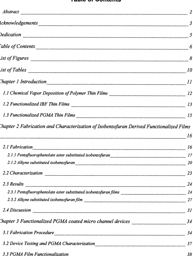
The starting functionalized materials were deposited using CVD. The methodology for the CVD process is straightforward and well documented. In a typical CVD process the chosen substrate is exposed to one or more volatile precursors, which react and decompose on the substrate surface to produce the desired deposit. Frequently, volatile byproducts are also produced, which are removed by a gas flow through the reaction chamber. Schematic of a typical CVD system is shown in Figure 2. In a CVD system, a precursor container with the monomer is kept at an elevated temperature to achieve vaporization. From the precursor vessel, the vapor flows through a heated quartz tube into the tube furnace. In the furnace, the monomer undergoes cracking, forming a reactive intermediate species, ready for polymerization. After the furnace, the vapor is flowed through a heated line into the
deposition chamber. In the deposition chamber, the precursor is deposited and polymerized on the chilled surface of a substrate. In sections 2.1.1 and 2.1.2 we describe the fabrication details for the two functionalized films.
I Initiator 1PO.. [~~"", MC L . ...,nwto
am$
'heated lines oated sor JarDry Pumrp Exhaust
Figure 2. Diagram of CVD system.
2.1.1 Pentafluorophenolate ester substituted isobenzofuran
Scott Meek has synthesized both monomers used in this work in the professor Tim Swager lab in Department of Chemistry at MIT. In Figure 3, a scheme of the synthesis for the pentafluorophenolate ester substituted monomer is shown. The synthesis is briefly described here. For a detailed procedure of the synthesis, see Appendix A
1,2,5-tribromobenzene was dissolved in dry toluene together with furan under argon. The solution was cooled and nBuLi in dry hexane was added dropwise. The reaction proceeded at room temperature overnight. Afterwards, the solution was diluted with dichloromethane and washed with distilled water, and then dried with MgSO4 and concentrated over a rotary evaporator. The resulting oil was purified over a silica gel column with dichloromethane, to
give bromo-epoxynaphtalene. The bromo-epoxynaphtalene was dissolved in dry THF under argon and cooled using a dry ice bath. nBuLi was added dropwise and CO2 gas was bubbled through the solution. The solution was then poured into a mixture of ether, ice, and concentrated HCl. The solution separated, and the aqueous phase was washed with ether. The combined organic layers were dried with MgSO4 and concentrated on a rotary evaporator. This gave the epoxynaphtanoic acid. The epoxynaphtanoic acid was dissolved in dry
dichloromethane under argon. Then 1-(3- dimethylaminopropyl)-3-ethylcarbodiimide hydrochloride
EDAC-HCI, pentafluorophenol, and DMAP were added and the solution was stirred. The reaction mixture was then diluted with dichloromethane and was washed with HCL, NaOH and brine. Concentration on the rotary evaporator gave light yellow oil that was taken up in ethyl acetate. Pd/C was added and the mixture was transferred to a hydrogenerator vessel overnight. The solution was then filtered and concentrated.
Over time, pentafluorophenolate ester substituted monomer which was stored in a glass vial exposed to air, crystallized and changed its physical state from being a yellow liquid into being a white solid powder. The final powder state can be seen in the right vial in Figure 4. This phase transition did not appear to have any noticeable impact on the fabrication of the films.
O
Br n-BuLi, Furan - B1. nBuLi
IOH
Br PhMe, -20 OC -r.t. 2.CO2 67% 3. H+, H20 1 90% 2 1. EDAC-HCI, DMAP Pentafluorophenol 2. H2 Pd/C 9.4 /O F F
Figure 3. Synthesis scheme of pentafluorophenolate ester isobenzofuran monomer. J3 19
Figure 4. Left vial contains alkyne substituted monomer. Right vial containss pentafluorophenolate ester substituted monomer in the powder state.
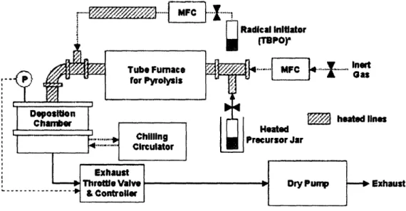
Polymerization of pentafluorophenolate ester substituted monomer proceeds similar to polymerization of the unsubstituted monomer as shown in Figure 1. Polymerization was performed by cracking the functionalized 1,2,3,4-tetrahydro-1,4-epoxynaphthalene in a CVD system. The CVD system, Figure 5, was composed of a monomer delivery (vaporization) zone, pyrolysis zone, and deposition zone. The precursor monomer was placed in a glass vessel heated to 60 oC. The phase transition temperature was measured with theral gravity ananlysis (TGA). The vapor was flowed through a 1-inch diameter quartz tube in a Lindberg tube furnace (Watertown, WI) where the temperature was controlled to be between 550-700
oC. Reactive intermediate species, substituted IBF precursors, were produced by pyrolysis in the tube furnace and then flowed to the deposition chamber (10 inch diameter and 5 inch height) through a heated line (T = 110 °C). The line was heated to minimize polymer deposition on the walls. Ethylene gas, produced as a pyrolysis by-product shown in Figure 1, was vented to the exhaust. The pressure within the chamber was set at 0.2 torr by an exhaust valve (Type-253, MKS Instruments, Andover, MA) connected to an exhaust valve controller (Type-252, MKS Instruments, Andover, MA). The stage temperature of deposition chamber
was maintained at 150 C by circulating chilled water through internal coils on the backside of the deposition surface. Silicon wafers (p-type, 100), purchased from Montco Silicon Technologies, Inc. (Spring City, PA), were used as substrates for polymer deposition. Thickness of the growing film was monitored in situ by a small interferometer laser system.
Mass Flow Controllers Control units ~ ~. Computer Tor
Data Acquisition Dry Pump Control
Laser/Detector for interferometry SFurnace for Thermal CVD * Reactor Chamber Ckillr 4fr lling Stage Temperature
Iling Stage Temperature
Figure 5. Chemical Vapor Deposition system setup in the Institute for Soldier Nanotechnologies.
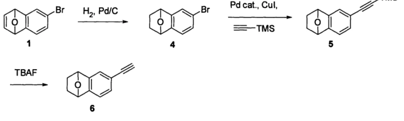
2.1.2 Alkyne substituted isobenzofuran
The scheme for synthesis of the alkyne substituted isobenzofuran monomer can be seen in Figure 6. The first step in the synthesis is the same as for the pentafluorophenolate ester substituted monomer, leading to the formation of epoxynaphtalene. The bromo-epoxynaphtalene was mixed with Pd/C in ethyl acetate. The mixture was added to a pressure vessel, degassed, and then filled with hydrogen gas. The solution was rocked under pressure,
and then pressure was released and solution was filtered. The filtrate was concentrated and then purified with a silica gel column in hexane:ethyl acetate. Pd(PhCN)2C1 2, P(tBu)3, and CuI were added to a shlenk line in a nitrogen glovebox. The flask was removed from the box and placed under argon. The product from the previous step dissolved in TiPS-acetylene and then added to the flask. The mixture was stirred at room temperature. The mixture was then diluted with EtOAc and filtered through a plug of silica. The filtrate was concentrated and purified over silica gel in hexane:EtOAc. The resulting product was dissolved in THF together with TBAF, and the mixture was stirred at room temperature. The mixture was then concentrated and purified over silica gel hexane:ethyl acetate), leaving a dark yellow oil, Figure 4. A complete synthesis procedure can be found in Appendix B.
TMS
Br H2, Pd/C Br Pdcat., Cu,
1 4 5
TBAF
6
Figure 6. Synthesis scheme of alkyne isobenzofuran monomer.
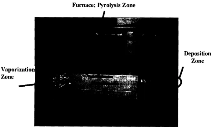
Only small quantities of the alkyne substituted monomer were available for deposition. As a result, a small home-made CVD setup was employed. The system is pictured in Figure 7. This system consisted of a 1 inch quartz tube (Quartz Plus Inc, Brookline, NH) divided into a monomer vaporization section, a heated zone for monomer cracking, and a deposition section. The system also contained a pump, and control panels for regulating the temperature and pressure (not pictured in Figure 7). Monomer was placed on an aluminum boat in the vaporization section on the far left of the quartz tube as shown in Figure 7. Based on TGA transition temperature, the vaporization temperature for the monomer was set at 800 C. The
quartz tube then passed through the furnace, which was heated to 600' C. High temperature was used for monomer cracking. Silicon substrates were placed parallel to the gas flow on the far right of the quartz tube, Figure 7. Temperature in the deposition zone was not controlled but is believed to be near ambient when tube is uncovered. To achieve a slightly higher temperature, aluminum foil was wrapped around the quartz tube. Pressure in the system was held at 0.4 torr using a vacuum pump. There were no means for monitoring the growth of the film in-situ, as a result, the film thickness was measured post-deposition by ellipsometry.
Furnace; Pyrolysis Zone
I
Deposition Zone Vaporizati
Zone
Figure 7. Chemical Vapor Deposition system setup used for alkyne substituted isobenzofuran films.
2.2 Characterization
Deposited films were extensively tested using several characterization methods. The deposition thickness of the pentafluorophenolate ester substituted films was monitored in-situ by an interferometer using 632.8 nm He-Ne laser light (JDS Uniphase, San Jose, CA). A cycle thickness was calculated by dividing the total film thickness (based on profilometry measurements) by the number of cycles on the interferometer. For the pentafluorophenolate ester substituted film, gel permeation chromatography (GPC) was used to measure molecular weight and nuclear magnetic resonance (NMR, Varian Mercury 300), was used to identify the chemical structure of the film. Surface morphologies were analyzed with optical microscope and with a NanoScope III atomic force microscope (AFM) (Digital Instruments) operating in tapping mode. The surface composition was quantified by X-Ray Photoelectron Spectroscopy measurements (XPS) obtained with a Kratos Axis Ultra Spectrometer (Kratos Analytical, Chestnut Ridge, NY) equipped with a monochromatized Al Ka X-ray source. Pass energies were 160 eV for survey scans.
A variable angle spectroscopic ellipsometer (MO-2000 WVASE32 J.A. Woollam Co., Inc at the ISN) was used for measuring the thickness of the alkyne films and the refractive index over a wide range of wavelengths. Raman spectroscopy was employed to show the presence of carbon triple bonds on the polymer surface using Hololab 5000R: Modular Research Raman Spectrometer with Microprobe (Kaiser Optical Systems, Inc., Ann Arbor, MI). Standard Raman spectroscopy of alkyne films on a clean silicon substrate did not resolve the alkyne peak, since the signal from the silicon substrate overlapped the weaker signal coming from the alkyne bond on the film surface. In order to address this issue, we used a Klarite (Mesophotonics Ltd.) substrate for deposition, see Figure 8. These substrates feature a sub-micron scale patterned gold-coated silicon surface, comprised of a regular array of holes. The surface pattern functions as a photonic crystal leading to formation of surface plasmons, which, in turn, govern the Surface Enhanced Raman Spectroscopy (SERS) amplification. This increases the sensitivity of the measurement by many orders of magnitude and extends
the range of Raman measurements to as low as part-per-billion levels. These substrates have proven very useful for thin films that otherwise would only give off a very weak signal. Furthermore, these substrates are currently under development for further optimization23
Figure 8. Klarite substrate: a micro patterned gold coated silicon surface covered by a self assembled monolayer of benzothiol.
2.3 Results
2.3.1 Pentafluorophenolate ester substituted isobenzofuran films
When observing the films under optical microscopy, films appeared to be smooth and without any visible pinholes. Profilometry and AFM were also performed to confirm film smoothness (results not shown). In situ interferometer of the deposition system was
calibrated using profilometry thickness measurements. A cycle thickness was calculated by 24
dividing the total thickness by the number of cycles of the interferometer. For a typical film, the thickness was 500 nm, after 1 hour of deposition. The growth rate was 0.3 A/s.
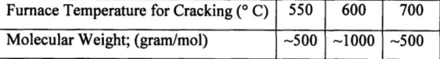
Molecular weight of the resulting pentafluorophenolate ester substituted films was obtained using GPC with tetrahydrofuran (THF) as a solvent. The maximum observed number average molecular weight was 1000 g/mol for a furnace temperature of 6000 C. Cracking the monomer at the lower 5500 C and the higher 7000 C furnace temperatures showed a decrease in the number average molecular weight of the deposited material, as can be seen in Table 1. With a molecular weight of the monomer of 266 g/mol these averages correspond to only a few units of the IBF functionalized monomer units. Thus, the films appear to be made up of small oligomeric deposits, as apposed to an ideal high molecular weight polymer chains. Note that film mechanical properties depend strongly on and vary considerably with molecular weight. Therefore, these films would likely be lacking in both strength and toughness
Furnace Temperature for Cracking (o C) 550 600 700 Molecular Weight; (gram/mol) -500 -1000 -500
Table 1. Number average molecular weight of the deposited film at different cracking
temperatures.
The XPS spectrum for a film made at a furnace temperature of 600' C is shown in Figure 9. From this spectrum, we can calculate atomic concentrations for fluorine, carbon, and oxygen atoms. Table 2 shows the calculated atomic concentrations and those expected from stoichiometry of the polymer unit. Based on values in Table 2, we calculated that at 6000 C, 90 % of the original fluorine remained on the film surface post deposition. However, when
furnace cracking temperature was held at 7000 C only about 25% of the fluorinated groups remained on the surface, while the remainder of ester bonds broke during cracking.
Table 2. Atomic
surface.
concentration percentages on pentafluorophenolate ester substituted film
V
4 i/
/
I [./
,
I;S
'
|~ , , ,. . . ... . .. ,.• 1000 800S 600Binding Energy (eV)
400 0
Figure 9. XPS spectrum of the pentafluorophenolate ester substituted film (furnace temperature 6000 C). The XPS spectrum is a survey spectrum, a high resolution spectrum could not be collected due to charging of the polymeric film surface.
26 Stoichiometric At 6000 C At 7000 C Fluorine 22 19.6 5 Carbon 65 68.8 N/A Oxygen 13 11.6 N/A - - -- .... I • . , . . ' . I
I
' IThe H' NMR spectrum (not shown) of the pentafluorophenolate ester substituted polymer is in agreement with the NMR spectrum collected for the monomer. There is no indication of contamination.
2.3.2 Alkyne substituted isobenzofuran film
The alkyne substituted films were studied under optical microscope (Figure 10). The film thickness of all films varied over the length of the substrate, decreasing in the direction of the flow (Figure 11). The average thickness was measured to be approximately 130nm after one hour for a film deposited at ambient temperature. The films appeared smooth to the naked eye. However, when observed in an optical microscope(Figure 10, row 1), the surface of these films was covered with microdefects uniformly spaces over the entire substrate surface. Films deposited at a slightly higher temperature were much thicker, which thicknesses ranging between 350 nm down to about 140 nm. On these films, macrodefects could be seen with the naked eye (Figure 11). The large smooth domains in these films did not contain any microdefects.
Figure 10. Optical microscopy pictures of the surface of the alkyne substituted polymer film. (Vaporization temperature 800 C; cracking temperature 6000 C). Top row shows a film
deposited in ambient temperature. Middle and bottom row show two films deposited at a slightly higher temperature. Aluminum foil was used to cover the deposition tube in order to increase the deposition.
Figure 11. Picture show silicon substrates with deposited alkyne substituted films.
(Vaporization temperature 800 C, cracking temperature 6000 C). From left to right: (1) film
deposited under slightly elevated temperature, with visible macrodefects, (2) film deposited under slightly elevated temperature, with visible macrodefects. Film deposited under ambient temperature, (microdefects). Interference fringes show the variation in the film thickness.
Optical properties of the alkyne substituted film were also investigated. The variation of the refractive index, n, with wavelength for different deposition temperatures are shown in Figure 12. n is the refractive index indicating the phase velocity for the material; k is the extinction coefficient, which indicates the amount of absorption loss when the electromagnetic wave propagates through the material. Both n and k depend on wavelength. For both n and k, values below 300 nm are somewhat uncertain due to absorption in the film. The alkyne films appeared to be transparent in the visible and the near IR range, where the upper limit of the instrument range was reached.
Z.6 -n 2.4 k 2.2 c 2.0 1.8 1.86 1.05 1.80 1.75 1.70 1.85 l.5 1.2 0.9 0.6 *1 0.3 0.0 200 400 600 800 1000 a Wavelength (nm) , 10.14 1.60 10.08 n 0.12 0.10 1.55 ... k 006 -0.08 -0.08 1.50 0.06 C 0.04 0.04 1A45 0.02 " -0.02 0.00 1.40 1.601 200 .300 400 500 . .. 600 700 800 900 1000 .. .- 0.02 200 300 400 500 600 700 800 900 10000.00 b wavelength (nm) C wavelength (nm)
Figure 12. Refractive index n and extinction coefficient k as a function of wavelength for the alkyne substituted films. (a) Film deposited at room temperature. (b) Film deposited at elevated temperature, data taken at thin end of film. (c) Film deposited at elevated temperature, data
taken at thick end of film.
To perform GPC, polymer films have to be dissolved in an organic solvent such as THF or dimethylformamide (DMF). Since the films were not soluble in either of these solvents, we were unable to obtain the number average molecular weight of the alkyne films.
Typically, the C-C triple bond of free alkynes is observed around 2200 cm- in traditional Raman spectroscopy. Surface enhanced Raman measurements of the alkyne functionalized films (Figure 13) shows a peak at 2107 cm-1, that can be assigned to the alkyne groups on the film surface. The variation is likely due to the change in the local chemical environment.
30
Figure 13. SERS spectrum collected for alkyne films deposited on Klarite substrate.
2.4 Discussion
We have developed pentafluorophenolate ester and alkyne functionalized isobenzofuran thin film coatings. Polymerization of the pentafluorophenolate ester substituted monomers proved to be difficult in the temperature range of 550-7000 C, with best results obtained at 6000 C. We postulate that since pentafluorophenolate ester functional groups are bulky, it is likely that they prevent the furan groups from coming in close enough proximity to each other for polymerization to occur. In addition, we demonstrate that at 7000 C, the optimal cracking temperature for the parent IBF material, the ester bonds holding the fluorinated functional group decompose. At a slightly lower temperature of 6000 C, we were able to
4oW woo lowo 0 a 1000 ao 03 -i ' -•,r :,•• ., .. • ,••••. ,,.
preserve surface functionalization, however, we observed only marginal polymerization of the monomer units. As a result we were unable to find a cracking temperature that would both allow for deposition of pentafluorophenolate ester and also preserve polymer functionalization.
Polymer film deposition of the alkyne substituted IBF was achieved only at the cracking temperature of 6000 C. At this condition, using surface enhanced Raman spectroscopy, we determined that the alkyne functionalization was preserved for further use in click chemistry. However, all of the films contained either micro or macro sized defects depending on the deposition temperature. Specifically, at ambient deposition temperature, films were covered with micron sized defects. Similar defects were observed in the parent material when cracked at 6000 C instead of the optimal 7000 C. Choi et a1'9 postulate that in the parent material, these defects are caused by various unreactive species that provide unfavorable environment for the growth of the polymer film. A proposed mechanism of the defect formation during polymerization is shown in Figure 14. Accumulation of the unreactive species on the surface leads to no or very little film deposition in these areas. As a result, there will be generation of defects, as observed under optical microscopy, Figure 10. In addition, in our case, it is possible that crosslinking of the alkyne groups on the functionalized polymers can further enhance microdefect formation. Film crosslinking is corroborated by the facts that, unlike the parent material, alkyne functionalized films do not dissolve in common organic solvents. At higher deposition temperature, we observe that film subdivide into two domains, one smooth with no observable defects, and a second completely covered by defects. At this time we do not have a good understanding of what causes this change. In the future, optimal conditions for cracking and deposition will need to be further investigated. The presence of crystals in the finished films is not desired.
The parent PIBF material has excellent optical properties, including a high refractive index (n = 1.63 at 633 nm) and transparency in the visible and the near infrared spectral range. For the alkyne functionalized films, we observed slightly higher refractive index (n = 1.67 at 633
nm, measured for the film fabricated at ambient deposition temperature) and similar transparency in the visible and near IR. These optical characteristics can be exploited in combination with surface modifications to create waveguide based biological sensors. Such biosensors can be integrated in a micro fluidic device where optical properties of the sensor surface would be modulated by changes in the local fluid environment. For example, changes can be caused by variation in local pH, surface adsorption, and other biochemical
interaction with the functionalized film coating.
o acltie spees
o unreactive species
"0 growing polymer chain
O c
diffusion anrd / deactivation
>4
n
-advorpt ion desorptlon
0 0 0 diffusion and , polymer nucleation I Ib)
defect
0
0
10 I" OO f) (C) econdary adsorption of actle species 0 00 on defect domain polr 0 O
d)growth /
ppoflmoer
govnUi
on d:*foe
Arnýa
Figure 14. Schematic illustration of growth and defect formation in the parent PIBF material. (reproduced from Choi et all).
Chapter 3
Functionalized PGMA coated micro channel devices
The main objective of this part of the thesis has been the development of functional coatings for microfluidic applications in PDMS devices. In particular, we deposit PGMA polymer thin films on patterned PDMS substrates using initiated chemical vapor deposition. We show that the epoxide groups in PGMA can be used for bonding of the PDMS substrate to glass by UV initiation. Furthermore, we show that most epoxide groups remain on the surface post bonding and can be further employed for surface modification.
3.1 Fabrication Procedure
PDMS stamps with predefined micro fluidic channels were fabricated using standard soft lithography procedures with a SU8 patterned silicon master22. We used straight rectangular channels 2mm wide, 100 micron deep, and 3 cm long. After curing, the PDMS stamps were pealed from the master and cut into standalone devices. Openings for the inlets and outlets were punched through at both ends of the PDMS channel. Then these PDMS substrates and glass slides were placed in an initiated hot filament CVD (iCVD) reactor for thin film deposition24.In Figure 15, a picture of the reactor is shown. In a typical hot filament CVD (HFCVD) reactor, vaporized monomer is pumped into the chamber where it decomposes over the hot filament to form active precursor species that polymerize on the cooled substrate surface. iCVD is a subset of HFCVD in which a free radical initiator is added along with the monomer to allow cracking at a lower temperature and therefore to prevent degradation of temperature sensitive monomers.
Figure 15. HFCVD reactor.
Glycidyl methacrylate (GMA, Fluka), Figure 18, was vaporized at 720 C and delivered at 2.0
sccm through a MKS 1153 mass flow controller. The initiator di-tert-butylperoxide (TBP, Aldrich) was vaporized at room temperature and delivered at 0.6 sccm through a MKS mass flow controller. The PDMS and glass slides were chilled on the back side to 300 C, however, their actual temperature was not measured. We expect their temperature to be higher than the chiller temperature. Generally, two PDMS substrates along with two glass slides were coated at the same time Figure 16. Furthermore, a small piece of silicon was placed on the deposition surface for real time deposition monitoring with laser interferometry. The system was pumped down for one hour or until gas bubbles trapped between the stage and the PDMS had disappeared. Hereafter, the GMA monomer was flowed into the reactor until the pressure reached 2 torr, at which point the flow of the monomer was stopped and the exhaust valve was closed. To pre-soak the PDMS with monomer, the reactor was allowed to remain at this condition for one hour. After this, the deposition was started. First, the monomer was flowed in at 2.0 sccm for 10 minutes while the pressure was reduced to 400 mtorr to remove all oxygen that may have leaked into the system while the exhaust valve was closed. Second,
36
the TBP flow was started at 0.6 seem and the 0.5 mm tungsten filaments were heated to 800 C. We varied the deposition time between 60 and 120 minutes. To remove unreacted GMA
monomer in PDMS, the chamber was pumped down to 8 mtorr after film deposition.
i jii j 1 0 0.
b
C
Figure 16. (a) Deposition of GMA to the glass slide and the PDMS substrates in the reaction chamber. (b) Coated substrates spaced by a thin film of ethanol. (c) Finished device, with PGMA coating uniformly covering the channel walls.
Schematic of bonding the PGMA coated PDMS devices to glass is shown in Figure 16. The PGMA coated glass slide was covered with ethanol to somewhat swell the polymer film in order to detangle polymer chains for bonding, and placed inside the iCVD reactor chamber. Then the PGMA coated PDMS device was placed on top of the glass slide. The pressure was prior to bonding reduced slowly to minimize the risk of PDMS sliding off the glass substrate. Generally, the chamber was pumped down for one hour to remove any visible ethanol and gas bubbles trapped between the glass slide and the PDMS. Afterwards, a handheld UV
37
lamp (UVLG-54, UVP) was placed 11.4 cm above the stage surface directly over the substrates to provide 60 ýpW/cm2 intensity at 254 nm. To determine the optimal time for irradiation, PGMA coatings were deposited on silicon and irradiated for 4-20 minutes under vacuum at the same conditions as described above. The chemical structure of the resulting films was examined using FTIR (not shown). Since the FTIR spectra did not vary, we chose an arbitrary time of 8-10 minutes for irradiation, to open up the epoxy groups and initiate the bonding.
3.2 Device Testing and PGMA Characterization
Polyether ether ketone (PEEK) tubing purchased from Upchurch Scientific was bonded using silicone glue and five minute epoxy to the inlets and outlets of the PGMA coated PDMS channels, see Figure 17 for the finished device. After the epoxy was cured, the durability of the device was tested. The inlet of the device was connected to a water filled vial. To modulate the water flow rate, the vial was connected to a compressed nitrogen gas cylinder
and the nitrogen pressure was varied.
38
We used several methods to characterize the resulting PGMA films on PDMS. First, the deposited film thickness was estimated. A small piece of unpatterned PDMS was placed under full vacuum for one hour to remove most of the gaseous contaminants and then weighed. After film deposition, the piece was pumped at full vacuum for about 30 hours to remove all unreacted GMA monomers from the PDMS and then weighed again. The overall estimated thickness was determined by dividing the total added mass by the exposed surface area of the PDMS piece. The chemical structure of the film was analyzed using nuclear magnetic resonance (NMR, Varian Inova 500).
3.3 PGMA Film Functionalization
To make surfaces hydrophilic, PGMA coated PDMS devices were modified with two different groups (Figure 18): hexamethylene diamine (HMDA, Sigma-Aldrich) and polyoxyethylene bis(amine) (PEG bis(amine), Sigma-Aldrich), using a method previously described in the literature23. The device was placed in a furnace and maintained at 700 C. A
0.5 M solution of HMDA or 0.1 M solution of PEG bis(amine) in ethanol was delivered to
the device using a syringe pump. At these conditions, the oxirane on the PGMA surface reacted with the primary amine on the functional groups to form a secondary amine and a P-hydroxyl group on the opened ring. Note that the nucleophilic attack in this reaction can be enhanced either through basic pH conditions or through use of a protic solvent. Ethanol was used in the current work. After functionalization, the channels were rinsed using ethanol.
(a)
(b)
(c)
Figure 18. (a) Chemical structure of the GMA monomer unit. (b) Chemical structure of the
hexamethylene diamine. (c) Chemical structure of the polyoxyethylene bis(amine).
The HMDA functionalized films were characterized using fluorescence microscopy. Since PEG bis (amine) functionalized films are not fluorescent, we developed an alternative method for characterizing the degree of surface functionalization. A bovine serum albumin (BSA) solution was flowed through the channels followed by a DI-water wash. BSA non-specifically binds to the hydrophobic PDMS and PGMA and to a much lesser degree to the hydrophilic polyoxyethylene bis(amine) functionalized surface. As a result, the difference in fluorescence was used as a rough estimate for the extent of functionalization, (not shown here).
In addition, the wetting properties of the films were tested. Using a pipette, a drop of water was placed in the channel inlet and the motion of the droplet was observed. If the channel walls were hydrophilic liquid would be drawn into the channel by capillary force. Both the uncoated PDMS, PGMA coated channels, and HMDA functionalized channels were tested.
3.4 Results
Literature value for the molecular weight of the deposited film under these conditions is in the range of 25-60 kDa24. The thickness of the films, based on weighing a piece of PDMS before and after polymer deposition, was estimated to be 1 and 2 microns, for one or two
40
hours of deposition, respectively. These are very rough estimates; however, since PDMS is a transparent polymer, we were unable to perform more accurate optical based measurements. Based on testing of the finished devices we found that 1 micron films were sufficient. As a result, all future experiments were performed with films deposited for one hour.
The FTIR spectra (not shown) of the iCVD deposited PGMA films deposited on silicon show narrow and distinctly resolved peaks characteristic of the chemical structure of the linear PGMA. Variation in the time of UV irradiation did not change the shift or the intensity of the IR peaks. Specifically, we considered peaks at 907, 848, and 760 cm-' that correspond to the glycidyl group. This also suggests that majority of the epoxy groups remained on the surface after UV irradiation. The finding that we verified by further reacting the epoxy groups with primary amines. An NMR spectrum collected for the PGMA, (Figure 19) compare well to the literature NMR spectrum of the GMA monomer24
to z dA. ... AP WIN... POCISi1NG RAI` It I~ Is :I, ,. , _ _. _ _•,_ _1a ._ _._ . -• . , 76 5 4 3 I I 0 ppn
Figure 19. H1 NMR spectrum of PGMA.
PGMA coated PDMS micro fluidic devices were pressure tested. They can withstand pressures up to 2 bar and can sustain flow rates as high as 10 mL/min over an extended
I is
41
period of time. Tests were carried out multiple times, and below 2 bars, not a single device leaked. This demonstrates that the binding between the two PGMA coated surfaces (PDMS and glass) is reliable. We speculate, that since most of the epoxide groups remain intact after UV treatment, as observed by FTIR, soaking the films in ethanol allows the polymer chains to entangle, minimizing the need for crosslinking.
When a water droplet was placed in the inlet of the pure PDMS or the non-modified PGMA coated PDMS channels, it remained stationary. When carefully pushed into the channel, the drop moved as long as the pressure was applied, but stopped immediately when the pressure was removed. On the other hand, when a water droplet was placed in the inlet of the HMDA treated channels it was drawn into channel and continued to move down the channel without external pressure. This demonstrates that functionalization of the films with HMDA makes the channel surface hydrophilic as compared to the intrinsically hydrophobic PDMS and PGMA coated ones.
Using fluorescence microscopy, devices at different stages of the fabrication process were examined. Comparison between the PGMA coated PDMS and the HGMA modified channels is shown in Figure 20. Devices coated with PGMA did not fluoresce, while the HMDA functionalized channels did. This corroborates the finding that indeed the functionalization was successful.
Figure 20. Fluorescence microscopy pictures showing the edge of a PGMA coated PDMS channel (left) and a PGMA coated PDMS channel modified HMDA (right).
Chapter 4
Summary and Outlook
In this work we explored chemical vapor deposition of functional thin film polymer coatings. First, we expanded earlier work on deposition of isobenzofuran thin films by functionalizing the starting material (1,2,3,4-tetrahydro-1,4-epoxynaphthalene) with two groups: pentafluorophenolate ester and alkyne. Deposition of the two monomers was performed using CVD, and the resulting films were extensively characterized. In the case of pentafluorophenolate ester functionalization, the films showed marginal polymerization. In the case of the alkyne functionalization, the films were polymerized with surface groups still present, but the films were also likely crosslinked. For films deposited at room temperature, the defects could only be observed under microscope, and were uniform over the entire surface. For films deposited at a higher temperature, the thickness of the films was increased, and the micro defects were no longer present. Instead, macrodefects could be seen with a naked eye. Optical characterization of the films showed that they retained interesting optical properties of the parent material including a high refractive index and transparency in the visible and the near-IR.
In the future, optimal conditions for deposition of the films can be explored. In particular, vaporization temperature, cracking temperature, pressure, substrate temperature, and time of deposition can be varied to better understand their influence on the film composition and defect formation. Furthermore, post deposition annealing processes can be investigated to enhance polymerization of the pentafluorophenolate ester substituted films. Making a blend of the two functionalized monomers with the parent material could also prove successful in enhancing mechanical properties of the film. Furthermore, modification of the functional groups needs to be explored to fully understand their potential for different applications.
43
In the second part of the thesis, we explored initiated hot filament CVD deposition of PGMA functional coatings in PDMS micro fluidic devices. We showed that PGMA coatings can be used for bonding of PDMS and glass coated substrates via UV initiation. The bonding was capable of withstanding pressures of up to 2 bar. Furthermore, we showed that majority of the functional groups remain on the surface and can be further modified by reacting the epoxy group on PGMA with a primary amine. Specifically, we made hydrophilic coatings by reacting PGMA with HMDA and PEG-bis(amine).
In the future, studies can be done to assess long term stability of the PGMA functionalized coatings. In particular, the influence of film thickness needs to be studied in greater detail. In addition, functionalization of PGMA coatings with PEG-bis(amine) can be explored in more detail. One potential application would be using these films as antimicrobial coatings for microfluidic devices.
Appendix A
Synthesis of pentafluorophenolate ester
IBF
Br
Br
Br n-BuLi, Furan PhMe, -20 °C - r.t. 67% 1 Br 1. nBuLi 2. CO2 3. H+, H20 90% O0 2 OH 2 1. EDAC-HCI, DMAP Pentafluorophenol 2. H2 Pd/C 53%Bromo-epoxynapthalene 1: 5.2 g of 1, 2, 5 -tribromobenzene were dissolved in 150 ml of dry toluene along with 22 ml of distilled furan under argon. This solution was cooled to -200 C and 60 ml of .257 M nBuLi in dry hexanes were added dropwise over 30 minutes. The reaction mixture was allowed to warm to room temperature, and was stirred overnight. The solution was then diluted with 150 ml of CH2C12 and was washed with 100 ml of distilled water. Drying with MgSO4 and concentration on a rotatory evaporator yielded yellow oil which was purified over a silica gel column with CH2C12 to yield 2.46 g of 1 as light yellow oil. (66.8% yield).
Epoxynapthanoic Acid 2: 2.46 g of 1 was dissolved in 125 ml of dry THF under argon, and this solution was cooled to -780 C in a dry ice bath. 47 ml of .25 M nBuLi were added
45
dropwise, and the solution was stirred at -780 C for 45 minutes. The argon was then turned off, and CO2 gas (from dry ice) was bubbled through the reaction mixture for 45 minutes. The solution was poured into 400 ml of ether with 185g of ice and 5 ml of conc. HC1. This solution was separated, and the aqueous phase was washed with 3x150 ml of ether. The combined organic layers were dried over MgSO4 and concentrated on the rototory evaporator to yield 1.9 g of 2 as a white/grey powder. (90% yield)
Pentafluorophenolate ester ester 3: 1.9 g of 2 were dissolved in 45 ml of dry CH2Cl2 under argon at 00 C. To this solution was then added 2.33 g of EDAC-HCl, 1.98g pentafluorophenol, and .255 g of DMAP. This solution was stirred at 00 C for 30 min. and room temperature for 4 hours. The reaction mixture was then diluted with 330 ml of CH2C 2 and was washed with 140 ml of 10% HCI, 140 ml of 5% NaOH, and 140 ml of Brine. Concentration on the rototory evaporator gave a light yellow oil which was taken up in 200 ml of ethyl acetate. To this solution was added .55g of 10 wt. % Pd/C, and the mixture was transferred to a hydrogenator vessel, and rocked under 38 psi of H2 overnight. This solution
Appendix B
Synthesis of alkyne
IBF
Pd(PhCN)2CI2, TiPS Br H2, Pd/C Br P(tBu)3, Cul 53% HN(iPr)2, dioxane 1 2 -- TiPS 3 73% TBAF THF 96%
Compound 2: 2.7 g of 1 were mixed together with .50 g of Pd/C (5 wt %) in 150 ml of ethyl acetate. The mixture was added to a pressure vessel, which was degassed and then filled with 35 psi of H2 gas. The solution was rocked under pressure for 14h. Afterward, the pressure was released and the solution filtered. The filtrated was concentrated, and then purified with a silica gel column (9:1 hexane:ethyl acetate). 1.48 g 2 as a clear oil were collected (54% yield).
Compound 3: .075 g of Pd(PhCN)2C12, .084 g of P(tBu)3, and .03 g of Cul were added to a shlenk flash in a N2 glovebox. The flask was removed from the box and placed under pressure of argon. 1.48g of 2 in 15 ml 1,4-dioxane were added along with 1.13 ml of diisopropylamine and 1.74 ml of TiPS-acetylene. The reaction mixture was stirred for 24h at room temperature. The mixture was then diluted with EtOAc and filtered through a plug of silica. The filtrate was concentrated and purified over silica gel (9:1 hexane: EtOAc). 1.65 g 3 as a dark oil collected (75% yield)
Compound 4: 1.65 g of 3 were dissolved in 33 ml of THF with 5.5 ml of 1.OM TBAF (in THF) and the reaction mixture was stirred at room temperature for lh. The mixture was then concentrated and purified over silica gel (9:1 hexane:ethyl acetate). .83 g of 4 were collected as a light orange oil (96% yield).
Bibliography
1 (a) Freund, L. B.; Suresh, S., Thin Film Materials. Cambridge University Press: Cambridge, U.K., 2003. (b) Macleod, H. A., Thin-Film Optical Filters. 3 ed.; Institute of Physics Publishing: London, 2001. (c) Kumar, S.; Nann, T., Small 2006, 2, (3), 316-329. (d) Gross, M.; Muller, D. C.; Nothofer, H. G.; Scherf, U.; Neher, D.; Brauchle, C.; Meerholz, K., Nature 2000, 405, (6787), 661-665.
2 (a) Krishnan S, Ward RJ, Hexemer A, Sohn KE, Lee KL, Angert ER, Fisher DA, Kramer EJ,
Ober CK Langmuir, 2006, 22 (26): 11255-11266 (b) Whitesides, G. M.; Ostuni, E.; Takayama, S.; Jiang, X. Y.; Ingber, D. E., Annual Review of Biomedical Engineering 2001, 3, 335-373. (c) Thompson, M. T.; Berg, M. C.; Tobias, I. S.; Rubner, M. F.; Van Vliet, K. J., Biomaterials, 2005,
26, (34), 6836-6845.
3 Olsson, Y. K., Chen, G., Rapaport, R., Fuchs, D. T., Sundar, V. C., Steckel, J. S., Bawendi, M. G., Aharoni, A., Banin, U., Applied Physics Letter, 2004, 85 (19) 4469
4 Whitesides, G.M. Nature Insights, 2006, 442, 7101
s Gunter, A., Khan, S. A., Thalmann, M., Trachsel F., Jensen K. F., Lab on a Chip, 2004, 4, 278-286
6 (a) Lee, J. N.; Park, C.; Whitesides, G.M.; Anal. Chem. 2003, 75, 6544-6554. (b) Vickers, J. A.,
Caulum, M. M.; Henry, C. S.; Anal. Chem., 2006, 78, 7446-7452
7 (a) Majid, N.; Dabral, S.; McDonald, J. F. J. Electron. Mater. 1988, 18, 301. (b) Senkevich, J.
J.; Desu, S. B. Thin Solid Films 1998, 322, 148. (c) Senkevich, J. J.; Mitchell, C. J.; Vijayaraghavan, A.; Barnat, E. V.; McDonald, J. F.; Lu, T.-M. J. Vac. Sci. Technol. A 2002, 20,
1445.
8 You, L.; Yang, G. R.; Lang, C. I.; Wu, P.; Moore, J. A.; McDonald, J. F.; Lu, T. M. J. Vacuum
Sci. Technol. A., 1993, 11, 3047.
9 Nichols, M. F. Crit. Rev. Biomed. Eng., 1994, 22, 39.
10 (a) Burns, M. A.; Johnson, B. N.; Brahmasandra, S. N.; Handique, K.; Webster, J. R.;
Krishnan, M.; Sammarco, T. S.; Man, P. M.; Jones, D.; Heldsinger, D.; Mastrangelo, C. H.; Burke, D. T. Science 1998, 282, 484. (b) Yang, X.; Grosjean, C.; Tai, Y.-C. Solid-State Sensor
and Actuator Workshop, Hilton Head Island, SC, June 8-11, 1998, 316. 1" Gaynor, J.; Desu, S. B. J. Mater. Res. 1994, 9, 3125.
12 Vaeth, K. M.; Jackman, R. J.; Black, A. J.; Whitesides, G. M.; Jensen, K. F. Langmuir 2000,