The Characterization of the Analog Devices Inc.
(ADI) Magnetometer
by
Jefri Mohdzaini
Submitted to the Department of Electrical Engineering and Computer
Science
in partial fulfillment of the requirements for the degree of
Master of Engineering in Electrical Engineering and Computer Science
at the
MASSACHUSETTS INSTITUTE OF TECHNOLOGY
Feb 2000
@
Massachusetts Institute of Technology 2000. All rights
A uthor ...
...
reserved.
ENG
MASSACHUSETTS INSTITUTE OF TECHNOLOGYJUL
27 2000
.... LIBRARIESDepartment of Electrical Engineering and Computer Science
Dec 16, 1999
Certified by
Certified by...
John Geen
Company Supervisor
Thesis Supervisor
Martin Schmidt
Professor
,Thesis, Supervisor
Accepted by ...
Arthur C. Smith
ilThe Characterization of the Analog Devices Inc. (ADI)
Magnetometer
by
Jefri Mohdzaini
Submitted to the Department of Electrical Engineering and Computer Science on Dec 16, 1999, in partial fulfillment of the
requirements for the degree of
Master of Engineering in Electrical Engineering and Computer Science
Abstract
The Analog Devices Inc. (ADI) magnetometer is a micromachined magnetic field sen-sor (MFS) that uses the Lorentz force to detect an external magnetic field. A circuit is designed to characterize the ADI magnetometer. The circuit does the following: drives an input into the magnetometer, and amplifies, rectifies and filters the mag-netomer's output. An average measured sensor output of 0.5mV was obtained in the presence of a bar magnet with a magnetic field of 8.2mT. The subsequent cir-cuitry (amplification, rectification and filtering) separates this output from interfering signals and raises its magnitude to about 150mV.
Thesis Supervisor: John Geen Title: Company Supervisor
Thesis Supervisor: Martin Schmidt Title: Professor
Acknowledgments
First and foremost, I would like to thank my supervisors at Analog Devices, John Geen and Steve Lewis, who were always around when I needed them. I can't ever thank them enough. I learnt so much from them in so little time.
I would also like to thank my MIT thesis supervisor, Professor Martin Schmidt, for his advice and quick turn-around time in helping me hand in this thesis in record time.
My utmost appreciation to John Chang who was always willing to help me with non-user friendly oscilloscopes, microscopes and spectrum analyzers; Esther Fong who walked me through the pains and tribulations of drawing figures in Adobe Illustrator; Nilmoni Deb who helped me with the formatting in ITEX. Chani Langford who helped scan in all my figures; and last but not least, all my workmates in the 4th floor ADI Cambridge lab who were very supportive and kept life in perspective. From them I learnt a backup career option: "And would you like fries with that?".
Contents
1 A General Overview of Magnetometers 9
1.1 The Underlying Mechanisms of Magnetometers . . . . 9
1.1.1 The Hall Effect . . . . 10
1.1.2 The Magnetoresistive Sensor . . . . 10
1.1.3 The Fluxgate Sensor . . . . 11
1.1.4 The Lorentz Force Mechanism . . . . 11
1.2 Patented Micromachined Magnetometers . . . . 12
2 The ADI Magnetometer 16 2.1 Structure of the ADI Magnetometer . . . . 16
2.1.1 Structure of the Sensor . . . . 16
2.1.2 Structure of the On-Chip Circuitry . . . . 18
2.2 The Mechanism of the ADI Magnetometer . . . . 18
2.2.1 The Underlying Mechanism of the Sensor . . . . 18
2.2.2 The Underlying Mechanism of the On-Chip Circuit . . . . 21
3 Characterizing the ADI Magnetometer 26 3.1 Designing the Driving Circuit . . . . 26
3.1.1 Calibration Technique . . . . 26
3.1.2 Calculating the Input Voltage . . . . 27
3.1.3 Calculating the Relative Displacement of the Sensor . . . . 31
3.1.4 Calculating the Expected Output . . . . 32
3.1.6 Method for Powering Up the Driving Circuit . . . . 36
3.2 Stage 2: Amplifying the Output of the Magnetometer . . . . 36
3.3 Stage 3: Rectifying the Amplified Output . . . . 36
3.4 Stage 4: Filtering the Rectified Output . . . . 37
4 Results and Discussion 38 4.1 Results of the Characterization . . . . 38
4.2 Discussion in Discrepancy Between Expected and Experimental Results 41 4.3 Recommendations . . . . 43
4.4 Sum m ary . . . . 44
List of Figures
1-1 UK Patent GB2,136,581 by F. Rudolf filed on March 7, 1984 . . . . . 13 1-2 European Patent EP389,390 by E. Donzier et al. filed on March 19, 1990 13 1-3 European Patent EP392,945 by E. Donzier et al. filed on October 17, 1990 14 1-4 US Patent US5,036,286 by Holm-Kennedy et al. filed on July 30, 1991 15
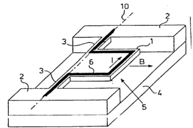
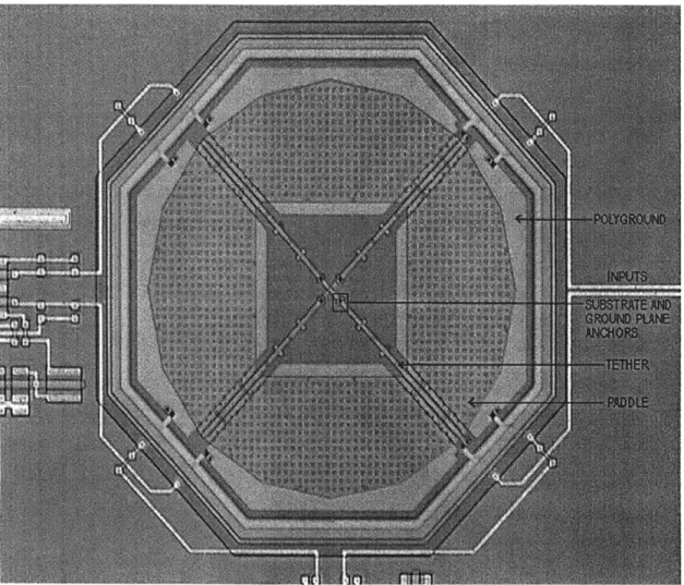
2-1 The ADI Magnetometer. The sensor is located in the center of the magnetometer while the inputs are on the right side of the magne-tometer. The on-chip circuitry located on the bottom and the left side of the magnetometer are identical to each other. The plane of the magnetometer is defined as the x-y plane. . . . . 17 2-2 Top view of the sensor. Since the only supports for the tethers are the
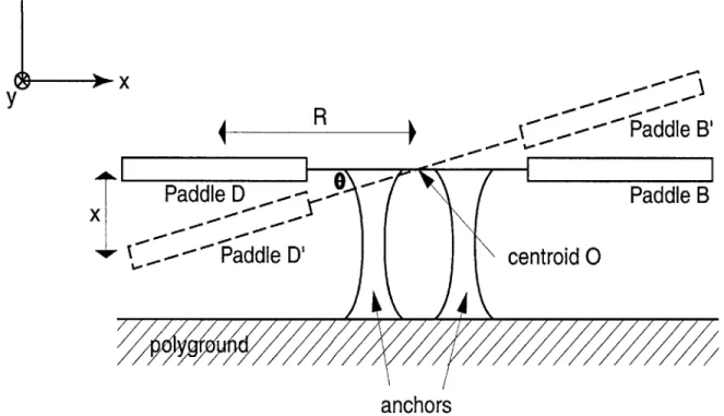
anchors in the center, the structure of the sensor is similar to that of an um brella. . . . . 19 2-3 Side view of the sensor . . . . 20 2-4 Route of current flow through the tethers and paddles. The dashed
line represents the current going through the polyground located un-derneath the tether. The solid line represents the current going through the tether... ... 22 2-5 Side view of the movement of paddles B and D to B' and D'
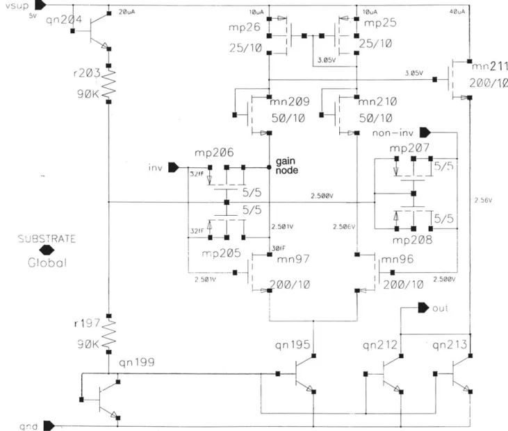
respec-tively in the presence of the Lorentz force. . . . . 23 2-6 Schematic of the on-chip circuit . . . . 24
3-1 The off-chip circuit. It has four stages (from left to right): the driving circuit, the amplifier, the rectifier, and the filter. The magnetometer
is located within the dotted lines. . . . . 28
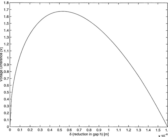
3-2 Plot of Voltage Difference vs. 6 (reduction in gap h) . . . . 30
3-3 A circuit model representing the relative displacement, A, and the out-put of the on-chip circuit . . . . 33
4-1 A sample output of the magnetometer, outl . . . . 39
4-2 A sample output of the amplifier, outla . . . . 39
4-3 A sample output of the rectifier, outir . . . . 40
4-4 A sample output of the filter, out1f . . . . 40
4-5 The magnetic field being bypassed away from the magnetometer chip due to the kovar leads. ... ... 42
List of Tables
4.1 Voltage outputs of the on-chip magnetometer (outi and out2), amplifier (outla and out2a), rectifier (outir and out2r) and filter (out1f and out2f) in mV (peak-to-peak). Outi measures the B-field in the x-direction while out2 measures the B field in the y-direction. . . . . 41
Chapter 1
A General Overview of
Magnetometers
The magnetometer is exactly what its name suggests it to be: a magnet meter. A magnetometer (also referred to as a magnetic sensor) measures the magnitude and direction of an external magnetic field. A magnetometer is useful in many areas, including navigation, automotive products and electronic devices.
The Analog Devices Inc. (ADI) magnetometer is a micromachined magnetic field sensor (MFS) which uses the Lorentz force to detect an external magnetic field. How-ever, before delving specifically into the ADI magnetometer, this chapter focuses on gaining a general understanding of the many different underlying mechanisms of mag-netometers, and also on providing some background research on patented microma-chined magnetometers.
1.1
The Underlying Mechanisms of Magnetometers
This section focuses on the classification, background, and the advantages and disad-vantages of various kinds of magnetometers. There are two main ways to classify a magnetometer:
2. Classification according to the underlying mechanism such as Hall effect, mag-netoresistive sensing, Lorentz force etc.
The more common classification in literature is the classification according to underlying mechanism. This chapter will elaborate on the more popular underlying mechanisms for the magnetometer: the Hall effect, magnetoresistive sensing, fluxgate, and the Lorentz force.
1.1.1
The Hall Effect
The discovery of the Hall effect by E.H. Hall in 1879 led to the birth of solid-state magnetic sensors. Hall was able to measure a cross-current in a thin gold layer on glass under the influence of a magnetic field. This was proof that the magnetic field exerts a force on the electric current in a conductor and not on a conductor itself, as was claimed by Maxwell[10]. The cross-current accumulates an excess charge, resulting in a transverse electrostatic field between the opposite edges of the gold layer.
However, there was not much progress on solid-state magnetic field sensors until the silicon-based integrated circuit (IC) technology came of age 30 years ago. Since the 1970s, the Hall effect has been the underlying mechanism of magnetic field sensors due to its cost-effective way of measuring magnetic fields in the range of 1mT.
The Hall sensors' range of 1mT is sufficient in most applications. For exam-ple, they can be used as non-contact switches, brushless electromotors (instead of commutators), and also to determine the position of the crankshaft in engines[7]. Unfortunately, for special applications such as the measurement of the deviation of the Earth's magnetic field or the measurement of biomagnetism, the Hall sensor's res-olution is insufficient. Besides poor resres-olution, the other problems with Hall sensors are the offset and the often limited dynamic range[6].
1.1.2
The Magnetoresistive Sensor
Magnetoresistive (MR) sensors are made up of thin strips of permalloy (NiFe magnetic film about 25nm thick). If a bias current is applied to the permalloy, the magnetic
flux across the permalloy will cause a change in resistance and therefore modify the current flow[1]. These MR sensors show sensitivities well below 10pT with a response time of less than ips. This allows for reliable magnetic readings in moving vehicles at rates up to 1000 times a second.
The MR sensor's high sensitivity, good repeatablity and small size make it ideal for navigation systems[2]. Other examples of the use of MR sensors in the past few decades is in the sensing of gear teeth on anti-lock breaks of automobiles, magnetic bubble memories, and read heads in the computer disk drive industry[3].
1.1.3
The Fluxgate Sensor
Compared to magnetoresistive sensors, the fluxgate sensor requires no electrical con-tacts to the magnetic material. This makes the fluxgate sensor easier to fabricate on a monolithic system consisting of a sensor and electronics on the same chip[5].
The fluxgate sensor consists of a core of magnetic material such as nickel-iron alloy surrounded by an excitation coil and a pickup coil. The excitation coil drives the core periodically into saturation and further decreases its magnetization. When an external changing magnetic field is applied to the core periodically, the differential permeability of the core varies periodically with the external changing magnetic field. This changing core magnetization induces a large voltage in the pickup coil[8].
In the 1970s, fluxgate sensors were popularly used in space missions and low-altitude satellites where ruggedness, stability and reliability were important factors. Nowadays, fluxgate sensors are predominantly used in high-resolution measurements of dc fields because they offer a resolution of better than 1 nT. The disadvantage is that the 3 dB frequency limit is of the order of 20 to 50 Hz and the sensor dimensions are of the order of 10 to 30 mm[11].
1.1.4
The Lorentz Force Mechanism
The Lorentz force is generated by the interaction of a defined current through a con-ducting beam and an external perpendicular magnetic field. The generated Lorentz
force causes a lateral displacement of the conducting beam. The displacement of the beam is converted into a capacitance change which is detected by an electronic circuitry. A sensitivity of up to 100pT has been demonstrated[4].
A majority of magnetometers use the Lorentz force to obtain a cantilever plate deflection. Cantilever-type magnetometers have many practical applications, ranging from micromirrors for spatial light modulation and deflection, optical shutters, chop-pers and swtiches, to HDTV and resonant subanogram discrete mass biosensors[9].
1.2
Patented Micromachined Magnetometers
Researching the patented literature on micromachined magnetometers is useful to gauge how the ADI magnetometer stands with respect to the other magnetometers in the industry. The following is a summary of the underlying mechanism of some patented micromachined magnetometers:
" UK Patent GB2,136,581 by F. Rudolf filed on March 7, 1984.
Please refer to Figure 1-1. The flap (1) contains a conductor (6) that carries a current i. An external magnetic field, B, will result in the Lorentz force (normal to the flap) causing the flap to turn about its hinge (3). The change in distance between the flap and the fixed plate (5) underneath it causes a capacitance change which is measured by an external circuit.
" European Patent EP389,390 by E. Donzier et al. filed on March 19, 1990. Please refer to Figure 1-2. A piezoresistive material is embedded on beams (5) and (6). In addition, there is also a current loop carrying current i in (5) and (6). An external magnetic field, B, will result in the Lorentz force twisting one side of the beam upwards and the other side downwards. The twisting of the beam will change the pressure throughout the piezoresistive material, thus creating a voltage drop across the material that is measured by an external circuit.
10
A#41
5
Figure 1-1: UK Patent GB2,136,581 by F. Rudolf filed on March 7, 1984
F
B
5 6
1
/
4/4-Figure 1-3: European Patent EP392,945 by E. Donzier et al. filed on October 17, 1990 Please refer to Figure 1-3. Two thin conducting layers (1) and (3) are separated by an insulating material (2) and they reside over a cavity. Layer (3) conducts a current i, while layer (1) is at a different voltage and acts as one end of a capacitor. Plate (14) is the other end of the capacitor. An external magnetic field, B, will result in the Lorentz force causing the three layers (1), (2) and (3) to move. The displacement of layer (3) will cause a capacitance change between layer (1) and plate (14) which is measured by an external circuit.
e US Patent US5,036,286 by Holm-Kennedy et al. filed on July 30, 1991.
Please refer to Figure 1-4. The magnetic material (1) is attached to a movable silicon device platform (2). An external magnetic field will cause the magnetic material to move from its original position. This movement causes a displace-ment in the device platform which is transduced into an electrical signal where a change in capacitance is measured.
Chapter 2
The ADI Magnetometer
The ADI magnetometer was designed by John Geen in March 1997 and has already been fabricated before the commencement of this thesis project. Before any char-acterization is possible, it is necessary to understand how the ADI magnetometer works. This chapter concentrates on gaining an understanding of the structure and underlying mechanism of the ADI magnetometer.
2.1
Structure of the ADI Magnetometer
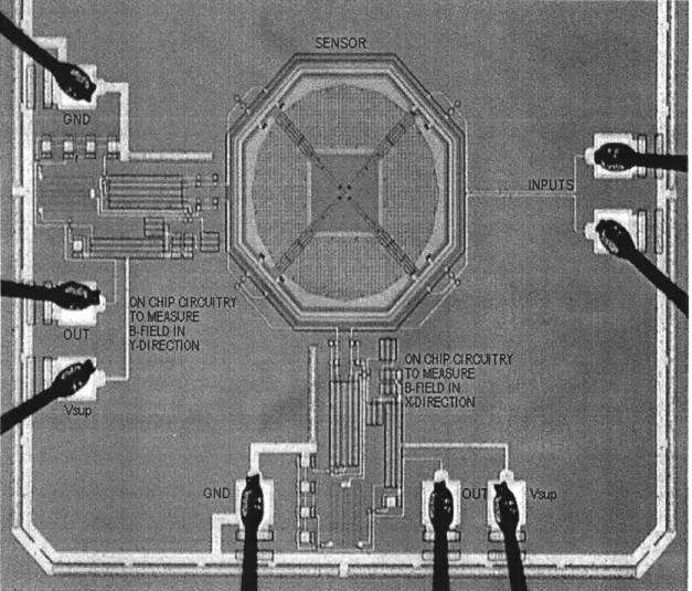
The ADI magnetometer consists of two parts (Figure 2-1): 1. the sensor located at the center of the magnetometer, and
2. the on-chip circuitry located around the sensor.
2.1.1
Structure of the Sensor
The sensor (Figure 2-2) is made up of four paddles and four tethers. Each tether is supported by a substrate anchor and a ground plane anchor located in the center of the sensor. Figure 2-3 shows the tether suspended in mid-air, exactly 1.6pm above the silicon polyground. As a consequence, the paddles, which are connected only to the outer end of the tethers, are also 1.6pum above the silicon polyground. This leaves the paddles free to tilt in a cantilever motion in the presence of the Lorentz force.
Figure 2-1: The ADI Magnetometer. The sensor is located in the center of the magnetometer while the inputs are on the right side of the magnetometer. The on-chip circuitry located on the bottom and the left side of the magnetometer are identical to each other. The plane of the magnetometer is defined as the x-y plane.
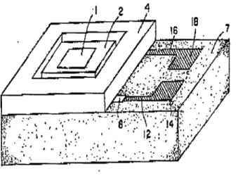
Figure 2-2: Top view of the sensor. Since the only supports for the tethers are the anchors in the center, the structure of the sensor is similar to that of an umbrella.
An easy way to understand the structure of the sensor is to think of an analogy between the sensor and an umbrella. The structure of the sensor can be thought of as similar to the structure of an umbrella where the anchors and tethers of the sensor are the frame of the umbrella, while the paddles of the sensor are the fabric of the umbrella. The paddles are free to tilt in the presence of the Lorentz force just as the fabric of the umbrella is able to tilt in the presence of a strong wind.
2.1.2
Structure of the On-Chip Circuitry
Referring to Figure 2-1, the on-chip circuitry consists of a square wave current input located to the right of the sensor, and two single ended outputs: the output below
polyground (Si) substrate
anchor ground plane anchor joint to tether paddle 1.6um I, N+
Figure 2-3: Side view of the sensor
the sensor measures magnetic field in the x-direction, while the output to the left of the sensor measures magnetic field in the y-direction.
2.2
The Mechanism of the ADI Magnetometer
The ADI magnetometer works on the principle of the Lorentz force: if a current i is driven along the paddle of length 1 with a magnetic field B present which is perpendicular and in the same plane as i , a Lorentz force
F = lI -
I
x B (2.1)is generated which is normal to both i and B.
This section studies in detail the underlying mechanism of how the sensor detects a magnetic field, outputs a corresponding electric signal, and how the on-chip circuitry amplifies this electric signal.
- -I- - 0 - - -P - - - - - - - - -
-2.2.1
The Underlying Mechanism of the Sensor
A square wave current is fed into the input ports of the ADI magnetometer. The current flow route for a half cycle is shown in Figure 2-4. For the other half cycle, the current flows in the direction opposite to the route shown in Figure 2-4.
The operation of the magnetometer is best described with an example. Please refer again to Figure 2-4. Assume that there is a magnetic field in the x-direction and that current is flowing around the magnetometer as shown. As a result of the Lorentz force, paddle D will move in the minus z-direction (into the page) while paddle B will move in the positive z-direction (out of the page). The Lorentz force does not affect paddles A and C because the magnetic field is parallel to the current flow of these plates.
Figure 2-5 shows from the side view, the movement of paddle D to D' and paddle B to B'. The gap between paddle D and the polyground is now smaller while the gap between paddle B and the polyground is now wider. Since the paddle and the polyground act as the two plates of a capacitor, this change in gap changes the capacitance of this capacitor. Since the voltage of the paddle and polyground remain the same, the charge on the paddle and the polyground changes when the capacitance changes. The amount of charge increases on the polyground below paddle D, while the amount of charge decreases symmetrically on the polyground below paddle B. The changes in the amount of charge on the two polygrounds are detected by the nodes inv and non-inv respectively on the on-chip circuit.
2.2.2
The Underlying Mechanism of the On-Chip Circuit
Figure 2-6 shows the schematic of the on-chip circuit. The on-chip circuit is basically a simple amplifier that amplifies the change in charge on the polyground. This section will first delve into how the nodes of the on-chip circuit are biased, and then proceed to give an example of how the on-chip circuit works.
y zx SENSOR 4i A A 2i 4i 2i 4i i D B < INPUT \4i 4i 2i C \ i i4
Figure 2-4: Route of current flow through the tethers and paddles. The dashed line represents the current going through the polyground located underneath the tether. The solid line represents the current going through the tether.
Z
x
R-- - ---R---
Paddle
B'
SPaddlePaddle
B
.- -~~Paddle
JD'
centroid 0
anchors
Figure 2-5: Side view of the movement of paddles B and D to B' and D' respectively in the presence of the Lorentz force.
vsup 5V an2 4 r203 90K n SUBSTRATE C9 b 0 197 90K qn
20uA 10uA 10uA
mp26 i mp25 25/10 25/10 mn209 KUmn210 50/10 M 50/10 mp206 i3nvF 5/5 -5/5 gain node 2.500V 2.50 IV 2.506V 30fF mpS 2 Kmn97 2 501V' U-200/10 3. 5V 40 non-Inv mp207
V
5/5 mp208 2/mn96 I 2.500V _200/10 oun qn 195 qn2121 qn213 199 qr-Figure 2-6: Schematic of the on-chip circuit
uA
mn 211
200/10
2.5 6V
Biasing the Nodes
V,, is powered up to 5V. The BJT qn199 is a diode connected bias transistor. Resis-tors r203 and r197 are placed in series with qn199 to act as a voltage divider and set the polyground (global substrate) at 2.5V. Besides that, each resistor's value of 90kQ ensures that a current of 20pA flows down the wire. The BJT qn204 is placed in series with qn199 to obtain symmetry in the voltage divider. The BJTs qn195, qn212 and qn213 mirror qn199 (since they all have the same base and emitter voltage) and
also pull down 20pA.
The FETs mp207 and mp208 are connected as back diodes. The back-to-back diodes permit rapid biasing of the nodes at DC. Because the equilibrium current to the node is only on the order of a few pA of leakage, the DC impedance (resistance) of the back-to-back diodes is considerably greater than their capacitive impedance. This is shown below:
=V D at DC where
kT= 25mV and iD is at most a couple of pA.
q
Therefore, the DC impedance (resistance) of the diode is on the order of 10GQ. On the other hand, with the circuit running at 1kHz, the capacitive impedance is:
1 =1.6GQ
100fFx27r-.khz =
Hence, the non-inv node is a high impedance and rapid biasing node biased at 2.5V. Consequently, FET mn96 has its gate biased at 2.5V and turns on, allowing current to flow from its drain to source. The same current that flows through mn96 also flows through mp25. Since FET mp26 is the current mirror of mp25 the same amount of current flows through FET mn97.
FET mn97 and FET mn96 have the same size and they both act as differential pair transistors as well as gain transistors. The inv node is biased at 2.5V, not only because of the symmetry of these FETs, but also because of the negative feedback
that happens from the output of the amplifier (the gain node) that stabilizes the working point. This amplifier is a pseudo-differential transcapacitance amplifier.
The FET mn211 is a source follower with its source connected to the output node. The FET mn209 acts as a spacer transistor to offset the V, of mn211 so that the voltage at the source of mn211 follows the gain node voltage. Since only a quarter of the current flows through mn209 compared to mn211, the width of mn209 is only a quarter of mn211. The FET mn210 is added to retain symmetry with mn209.
Example of the Mechanism of the On-Chip Circuit
Referring to section 2.2.1, let us assume that due to a tilt in the paddles there is an increase in the amount of charge by AVn in one polyground (connected to inv) and a decrease in charge by AVin, in the other polyground (connected to non-inv). Now the potential at inv is at +AVin and the potential at non-inv is at -AVi. The increase in potential at inv will pull more current (+gmAVin) through mn97, while the decrease in potential at non-inv will pull less current (-gmVin) through mn96 and also through mp25. Since mp26 is the current mirror of mp25, it will follow mp25 and pull (-gmAVin). The difference in current going into the gain node (-gmAVin from mp26) and out of the gain node (+gmAVin from mp25) forces the gain node to change its potential to satisfy Kirchoff's Current Law (KCL). The source follower mn211 will follow the change in potential of the gain node and pass the result to the output node.
Chapter 3
Characterizing the ADI
Magnetometer
This is where the thesis project begins. This chapter explains the calculation, design and implementation of an off-chip circuit that characterizes the magnetometer. The off-chip circuit is divided into four stages:
1. A driving circuit that powers up and drives the magnetometer.
2. An amplifier that amplifies the magnetometer's on-chip output. 3. A rectifier that transforms the amplified output to dc.
4. A filter that filters the high frequency noise of the rectified output.
3.1
Designing the Driving Circuit
3.1.1
Calibration Technique
A bar magnet is used as a convenient source of test magnetic field at a known distance. This was calibrated using a commercial gaussmeter. The magnetic field from the bar magnet is measured to be 8.2mT at 2cm.
3.1.2
Calculating the Input Voltage
Figure 2-4 shows the on-chip input voltage, V, directly connected to the sensor. In addition, the magnetometer in Figure 3-1 shows that the voltage of the sensor, Vsensor,
is half of V. Therefore, V can be obtained by computing Venso, first.
Since the voltage of the polyground, Voy, is already set at 2.5V by the on-chip circuitry (section 2.2.2), the main concern in building the driving circuit is in setting the voltage of the sensor, Vsensor. Ideally, the voltage difference between Vsensor and
V 01Y should be as large as possible. This is because the bigger the difference in voltage, the more charge is stored between the sensor and the polyground, which means the more sensitive the magnetometer will be to any movement of the sensor. However, there is a limit. Due to the difference in voltage, there will be an electrical force of
attraction between the sensor and the polyground. If the electrical force of attraction is bigger than the mechanical restoring force of the sensor, the sensor will collapse onto the polyground.
The optimal voltage difference, V, is calculated as follows: the electrical force of attraction, Fh, and the mechanical restoring force, Fm, are set equal to each other (equilibrium position) to find the optimal voltage difference, V.
Electrical Force of Attraction, Fh Fh =6 where
E = Energy stored in a capacitor = !CV2 2 2h y2 Therefore,
Fh= -E2 2 where
o= Permittivity of free space =8.854 x 1 V-2~ A = Area of 4 paddles = 156 x 10-9m2
V = Optimal voltage difference =
IVsensor
- Voly Ih = gap between the sensor and polyground = 1.6pum
Mechanical Restoring Force, Fm
CD o 0 i- CD CD~C CD -CD -1 CD 0 9 - '-CD CD Ft e+CD CD1 -- + CDCD U4 U5 U6 U7 U8 U9 ou 5V 226kn U9 330nF Okf2 LJ6A.. 10n 18.3kf2 1MD 226kf 2kf U5 20ko t1 outla In outir out1f0 2 1
DRVNGCRUI mgntmteswihndotdlie MPLFIR I RECIFERFITE
1 0kO U12a 5V Ula OV 1 kHz U2b NDQ 5V 10 1 % --15V 0 Ou Mq .5V
out2 out2a out2r out2f
Ukn d20k [ n226k- 10nF 1 U7 lOkk 26k2 lkf MU4 226k.Q 226kfl 20kflUQ 1 kW 1 kn U0 kc A A -60nF ~U6 +U + L460nF r330n U8 U2c 2kJo 83n 13kn 13kn 2k 0n 1 .k V V U b U2d 1 13 k 2610n 460nF j~j 226k<0 SU7 10kf2 10krl U3c 5V
r-/
-1*K = Mechanical Spring Constant of the sensor = Mw2 where
M = Mass of sensor = 1.07pig
w = Natural frequency of the sensor (translation along z-axis) = 27r -8.7kHz J = reduction in the original gap, h
Net restoring force, Fm + Fh = K6 + -cAV2
(h-6)2
At equilibrium position, Fm + Fh = 0. Rearranging the equation to obtain V in terms of 6:
2K
V= 1 (h2-262h+ 63) (3.1)
The graph of V vs. 6 is plotted from Equation 3.1.
The optimal voltage difference is just a little before the pull-in voltage at 1.67V. The pull-in voltage is when the sensor collapses onto the polyground. Hence, the further away from the pull-in voltage, the more robust the sensor is to shock. However, the trade-off is that less charge would be stored between the sensor and polyground, making the sensor less sensitive. Referring to Figure 3-2, the voltage difference, V, is chosen to be at 1.5V.
Therefore:
Vsensor = VOIY + V = 2.5V + 1.5V = 4V or
Vsensor = Voiy - V = 2.5V - 1.5V = 1V
The former is chosen because a higher voltage Vsensor would mean a higher input voltage, V. A higher V would enable more current to be passed through the sensor, making the sensor more sensitive to magnetic fields.
Hence, input voltage, V, (peak-to-peak):
1.8 1.7 1.6 1.5 1.4 1.3 1.2 1.1 1 0.9 0.8 0.7 0.6 0.5 0.4 0.3 0.2 0.1 0 C 1.1 1.2 1.3 1.4
Figure 3-2: Plot of Voltage Difference vs. 6 (reduction in gap h)
I I CD~ 0 C a) 40 0 0.1 0.2 0.3 0.4 0.5 0.6 0.7 0.8 0.9 1 8 (reduction in gap h) [m] 1.5 1.6 x 10⁶
--At this voltage, there is a change in gap between the sensor and the polyground by 6 = 0.27pm. The new gap, hN, (after powering up the input voltage to V) of the magnetometer is
hN = h - 6 = 1.6pm - 0.27pim = 1.33pum (3.3)
3.1.3
Calculating the Relative Displacement of the Sensor
Now that the voltage of the sensor, Vsensor, has been obtained, the relative displace-ment of the sensor, A, in the presence of an external magnetic field can be calculated. As shown in Figure 2-5, the sensor moves an angle 9 in the presence of the torque, T, of the Lorentz force about centroid 0. To find the relative displacement, A, 6 must be obtained first. This is done by using the rotational analog of Hooke's Law1:
T = KO - 0 where
KO = Angular mechanical spring constant = J - 2 47 x 10-1 N?, where
J = Moment of inertia about centroid 0 = 21.37 x 10- 18kgm2 w = Resonant frequency of the sensor = 27r x 7.45kHz
Rearranging the above equation to find 9: 0 - Ko r - 2-F.R _ 2-B-i-l-R Ko where
Ke
B = 8.2mT (magnetic field from a bar magnet used to provide a test field) i = 14 x 2 x 1k8 = 308A peak-to-peak2
1 = Length of paddle = 360pm
R = Distance from the center of mass of paddle to 0 (Figure 2-5) = 175pm Therefore, 0 = 6.77 x 10-rad
'Hooke's Law: F = k - x where F = force exerted on structure, k = linear mechanical spring constant of structure, and x = linear displacement of structure.
2
This is the current going through one paddle (hence the factor of 1/4) and is the peak-to-peak value of a current which is inverted each half cycle. The magnitude of current in each half cycle is
Since 6 < 1 and x < R, it can be approximated that:
0 = I- whereR
x = Displacement of sensor due to the Lorentz force (Figure 2-5)
Hence, the relative displacement, A, in the presence of a magnetic field, B = 8.2mT, is: X R - 0
A* = 0.89 x 10⁻³ (3.4)
hN hN
where hN = (h - 6) = 1.33pm (from Equation 3.3)
3.1.4
Calculating the Expected Output
Now that A has been obtained in the presence of an 8.2mT magnetic field, the cor-responding voltage output (on-chip), V0st, can be calculated. Figure 3-3 is a circuit
model relating the relative displacement of the sensor, A, to the output of the on-chip circuit. The values for the circuit devices are obtained as follows:
C= Capacitance from one paddle to the polyground = 'O'P = 0.26pF where
fo = Permittivity of free space = 8.854 x 1 0-12F
m
a= Area of 1 paddle = 39 x 10- 9m2
hN= 1.33prm
Capacitance from the polyground to the ground plane = pg = 9.4pF where
E = Permittivity of SiO2 = 3.27 x 10⁻¹¹ F
apg = Area of the polyground underneath 1 paddle = 49 x 10- 9m2 hpg = Gap between polyground and ground plane = 0.17pm
R =
2.3Mf1
Cp=
0.26pF
II
I~
I
C=
94fF
wvi
C
=
9.4pF
IVoutg.= 87pS
Figure 3-3: A circuit model representing the relative displacement, A, and the output of the on-chip circuit
I
Cm = Miller capacitance = Cmp206 + Cmp205 + Cmn97 = 94fF where
Cmp206, Cmp205 and Cmn97 are the cumulative capacitance of the inv node (Figure 2-6).
The values of the resistor, R = 2.3MQ, and transconductance, gm = 87pS are ob-tained from the simulation program ADICE. Therefore, the gain of this circuit is: Gain = R - gm = 200
The calculation of the change in the output voltage, Vot, proceeds as follows (please refer to Figure 3-3):
V,, = Gain-V1 = 200V1
V1 = C where
Cpg+Cm Gai~n
Q= V-A-Cp where
V= Voltage difference between the paddle and polyground = 1.5V (Section 3.1.2
A = 0.89 x 10⁻³ (from Equation 3.4) Hence, the output voltage:
Vot = 2.5mV. (3.5)
which is just within the range of detection, but not quantitative measurement, of an oscilloscope. Subsequent circuitry is implemented with a gain of 100 x 1 x 10 (from2 the amplifier, filter, and rectifier respectively) to bring the total gain to 500. Hence, the expected output is 1.25V.
3.1.5
Stage 1: Implementation of the Driving Circuit
The driving circuit is shown as part of the off-chip circuit shown in Figure 3-1. An H-switch (consisting of an ADG2123
device labeled U2a, U2b, U2c, and U2d) is built to drive the current back and forth through the magnetometer, simulating a square wave current input. A square wave input voltage (5V peak-to-peak from OV to 5V at 1kHz) from a signal generator, together with a complementary waveform from the ADG212 device labeled Ula is responsible for the switching of the H-switch. The 10kQ resistor acts as a pull-up enabling the use of switch Ula as an inverter, while the 3kQ resistor is added to prevent a short circuit in between switching. Because of the voltage drop across the 3kQ resistor, the power supply is increased to approximately 10.5V to maintain an 8V peak-to-peak square wave input at the node V (the input to the magnetometer).
As mentioned earlier, the 5V power supply biases the polyground at 2.5V (sec-tion 2.2.2) while the 10.5V power supply biases the input voltage at 8V, which in turn biases the sensor at 4V (section 3.1.2). The two power supplies have different time constants in powering up. To ensure that the difference in potential between the polyground and sensor is not more than 1.67V (the sensor will collapse onto the polyground if this happens; refer to Figure 3-2), a diode is placed between the 5V node and the V node. A diode is also placed between the 10V power supply and the 3kQ resistor. The next section explains the proper method of powering up the driving circuit to prevent the sensor from collapsing onto the polyground.
The outputs of the magnetometer (which is calculated in Section 3.1.4) are la-beled outl and out2 for detection of magnetic fields in the x-direction and y-direction respectively.
3
The ADG212 is a monolithic CMOS device comprising of four independently selectable switches. When the input is high, the switch turns on.
3.1.6
Method for Powering Up the Driving Circuit
First, the signal generator input is connected to Ula. Next, the 5V power supply is slowly powered up to 5V, making sure that the potential at the V node is following the potential at the 5V node with an offset of less than 1.67V. Then, the 10.5V power supply is slowly powered up until the voltage at the V node reaches 8V.
To turn off the circuit, the above steps are done in reverse.
3.2
Stage 2: Amplifying the Output of the Magnetometer
The amplifier inputs are nodes outl and out2 and the outputs are nodes outla and out2a. The OP074 devices labeled U4 and U5 amplifies the magnetometer on-chip outputs (outl and out2) by a factor of 100. The gain bandwidth product of the OP07 is typically 0.6MHz i.e. 6khz at a gain of 100. This is sufficient to suppress the high frequency and switching noise from the sensor. The 20kQ resistors ensure that the impedances facing the inverting and non-inverting nodes of U4 and U5 are symmetrical.
3.3
Stage 3: Rectifying the Amplified Output
The rectifier inputs are nodes outla and out2a and the outputs are nodes outir and out2r. The rectifier consists of the ADG212 device labeled U3a, U3b, U3c, and U3d,
and the OP07 devices U6 and U7. The ADG212 device acts as switches forcing the OP07 devices to have a gain of -1 during one half of the duty cycle and a gain of 1 during the other half of the duty cycle. This will rectify the square wave inputs outla and out2a into dc outputs (outir and out2r). Note however, that a factor of two in the output is lost after they are rectified.
The 460nF capacitors present at the outputs of U4 and U5 isolate the dc offsets from the inputs of the ground-referenced ADG212 switches (U3a, U3b, U3c, and U3d), minimizing the transient which must be handled by the buffer amplifiers U6 and U7.
4
3.4
Stage 4: Filtering the Rectified Output
The devices U8 and U9 form two-pole low pass filters with a dc gain of 10 and a pole frequency at 70Hz. The filters remove the ripple which is present on the outputs of the synchronous full-wave rectifiers leaving a dc voltage which represents the magnetic field.
Chapter 4
Results and Discussion
This chapter presents the results of the characterization of the ADI magnetometer, and discusses the differences between the calculated value and the experimental values obtained. Recommendations and suggestions for future work are also proposed.
4.1
Results of the Characterization
Referring to the circuit in Figure 3-1, sample outputs for the magnetometer outi, amplifier outla, rectifier out1r, and filter outif, are shown in Figure 4-2 to Figure 4-4 exactly as they appear on an oscilloscope.
Figure 4-1 and Figure 4-2 are ac coupled with their dc at 2.5V. Because of the noise present in these two outputs, it is difficult to measure with accuracy their change in voltage in the presence of the bar magnet (8.2 mT magnetic field). It can be seen qualitatively, however, that the peak-to-peak square wave gets larger in the presence of a positive magnetic field. In contrast, the peak-to-peak square wave gets smaller in the presence of a negative magnetic field.
Figure 4-3 and Figure 4-4 are dc coupled because the 460nF capacitors in the rectifier remove the large dc offset (Section 3.3). A positive magnetic field would increase the offset voltage, while a negative magnetic field would decrease the offset voltage. Hence, the change in voltage at out1r and out1f in the presence of the bar magnet can be measured with accuracy using a multimeter.
1md
tri d
Os 200s/d iv 2ms
Figure 4-1: A sample output of the magnetometer, outl
1v
tr d
-1v
fN\
Os 200s/d iv 2ms
Figure 4-2: A sample output of the amplifier, outla
1 V 200W /div trig'd -1v Os 200us /d i k)
Figure 4-3: A sample output of the rectifier, out1r
1eV 2V /div inoti trig'd I -10V Os 200jAs/dI v
Figure 4-4: A sample output of the filter, outif
40
/
2ms . vw wvw-d-NOIW %f
The results of the characterization of the ADI magnetometer are tabulated in Table 4.1. The -B field is -8.2mT and is obtained by turning the bar magnet around.
Device # 1 2 3 4 5 Field B -B B -B B -B B -B B J-B outi 0.5 -0.5 0.5 -0.5 0.5 -0.5 0.5 -0.5 0.5 -0.5 out2 0.5 -0.5 0.5 -0.5 0.5 -0.5 0.5 -0.5 0.5 -0.5 outla 40 -40 30 -30 30 -30 30 -30 30 -30 out2a 40 -40 30 -30 30 -30 30 -30 30 -30 outir 20 -20 15 -15 15 -15 15 -15 15 -15 out2r 20 -20 15 -15 15 -15 13 -13 13 -13 outif 200 -200 150 -150 160 -130 130 -130 140 -140 out2f 200 -200 150 -150 130 -160 150 -140 150 -160
Table 4.1: Voltage outputs of the on-chip magnetometer (outi and out2), amplifier (outla and out2a), rectifier (outir and out2r) and filter (outif and out2f) in mV (peak-to-peak). Outi measures the B-field in the x-direction while out2 measures the B field in the y-direction.
4.2
Discussion in Discrepancy Between Expected
and Experimental Results
As seen in the Table 4.1, the average output from the magnetometer, outi and out2, in the presence of the magnet bar is 0.5 mV peak-to-peak. This value is a factor of 5 lower than the calculated value of 2.5mV in Section 3.1.4.
The reason for this discrepancy is partly due to the packaging of the magnetometer which has kovarl leads. The kovar leads causes the magnetic field to bypass the magnetometer chip, as shown in Figure 4-5. Hence, the magnetometer chip does not receive the expected magnetic field of 8.2mT from the magnet bar.
Another reason for this discrepancy is that the peak-to-peak output from the magnetometer, e.g. outputl in Figure 4-1, is too noisy to be measured accurately. The oscilloscope reading could easily be off by a factor of 3.
The experimental amplified gain, outla and out2a, on average, is about 60. This
B
magnetometer
chip
B
X17
B
kovar lead
~.- pmagnetometer
chip
Figure 4-5: The magnetic field to the kovar leads.
being bypassed away from the magnetometer chip due
F---w
77q
F7 F77
is almost a factor of 2 less than the calculated amplified gain, which is 100, and the small signal amplification which was also measured to be 100. A possible explanation for the discrepancy is the non-linearity of the amplifier.
The experimental rectified output, out1r and out2r, is a factor of 2 less than the experimental amplified output, which is exactly what is expected.
The experimental filtered output, out1f and out2f, on average, is about a factor of 10 more than the experimental rectified output, just as expected. However, for device #3, #4, and #5, the filtered output due to magnetic field B is the inverse of the filtered output due to magnetic field -B. This is despite the response to the
±B fields symmetrical in the earlier stages of the circuit. Unfortunately, there was
no time to resolve this observation.
The experimental filtered outputs range from 200mV to 130mV, which means that the filtered outputs are not repeatable from device to device. This could be due to the difference of the position of the sensor (not exactly 1.6pm above the ground plane) from device to device. Another reason could be that the position of the magnetometer chip within the package is not well controlled from device to device, such that the kovar leads bypasses the magnetic field to different extents.
4.3
Recommendations
To obtain experimental outputs that are closer to the expected outputs, the kovar leads should be changed with leads which are not of ferro-magnetic material. Only then will the whole applied magnetic field, and not just a fraction of it, affect the
magnetometer chip.
In addition, the experimental values of the magnetometer output and amplified output have to be measured with more accuracy. This can be done with a digital oscilloscope with a sensitivity of up to 1mV. This would erase some uncertainty on the exact value of the experimental output.
4.4
Summary
The ADI magnetometer has been successfully characterized. A circuit has been built that does the following: drives an input into the magnetometer, and amplifies, rectifies and filters the magnetometer's output. The calculated (expected) sensor output in the presence of a magnet bar with a magnetic field of 8.2mT is 2.5mV. However, the experimental value obtained is 0.5mV. The subsequent circuitry (amplification, rectification and filtering) separates this output (0.5mV) from interfering signals and
raises its magnitude to about 150mV.
Although the test field (8.2mT) is large, the output signal (0.5mV) obtained is also large by the standards of micro-machined sensors. For example, the output of ADI's gyroscope is resolved to O.1pV. Therefore, the ADI magnetometer would definitely be able to detect magnetic fields of lower magnitudes. This thesis provides the ground work for further characterization of the ADI magnetometer.
4.5
Future Work
A different material for the sensor can be used to make a more sensitive magnetometer. The off-chip circuit and its corresponding power supplies can be miniaturized to make the whole magnetometer (inclusive of its driving circuit, amplifier, rectifier and filter) portable. This would make it easier to test the magnetometer with more accurately generated magnetic fields such as those from a Helmholtz coil.
Bibliography
[1] G. Bartington. Sensors for low level low frequency magnetic fields. In Low level low frequency Magnetic Fields, pages 2/1-2/9. IEE Colloquium, 1994.
[2] M.J. Caruso. Applications of magnetoresistive sensors in navigation systems. Society of Automative Engineers Publication, pages 15-21, 97602(1997).
[3] K.L. Dickinson. An introduction to high resolution patterned magnetoresistive sensors and their application in digital tachometers. In Pulp and Paper Industry Technical Conference, pages 31-36, 1994.
[4] H. Emmerich, M. Schofthaler, and U. Knauss. A novel micromachined magnetic-field sensor. In Micro Electro Mechanical Systems, pages 94-99. Twelfth IEEE International Conference, 1999.
[5] R. Gottfried-Gottfried, W. Budde, R. Jdhne, H. Kiick, B. Sauer, S. Ulbricht, and U. Wende. A miniaturized magnetic-field sensor system consisting of a planar fluxgate sensor and a CMOS readout circuitry. Sensors and Actuators A, 54:443-447, 1996.
[6] Zs. Kadar, A. Bossche, P.M. Sarro, and J.R. Mollinger. Magnetic-field measure-ments using an integrated resonant magnetic field sensor. Sensors and Actuators A, 70:225-232, 1998.
[7] S Kordic. Integrated silicon magnetic-field sensors. Sensors and Actuators, 10:347-378, 1986.
[8] F. Primdahl. The fluxgate magnetometer. J. Phys. E: Sci. Instrum., 12:241-253, 1979.
[9] B. Shen, W. Allegretto, M. Hu, and A.M. Robinson. CMOS micromachined cantilever-in-cantilever devices with magnetic actuation. IEEE Electron Device Letters, 17(7):372-374, July 1996.
[10] K. Russell. Sopka. The discovery of the hall effect: Edwin hall's hitherto un-published account, in c. 1. chien and c. r. westgate (eds.), the hall effect and its applications. Proc. of the Commemorative Symp., pages 523-545, 1979.
[11] K. Weyand and V. Bosse. Fluxgate magnetometer for low-frequency magnetic electromagnetic compatibility measurements. IEEE Transactions on Instrumen-tation and Measurement, 46(2):617-620, April 1997.