HAL Id: hal-01643511
https://hal.archives-ouvertes.fr/hal-01643511
Submitted on 21 Nov 2017
HAL is a multi-disciplinary open access archive for the deposit and dissemination of sci-entific research documents, whether they are pub-lished or not. The documents may come from teaching and research institutions in France or abroad, or from public or private research centers.
L’archive ouverte pluridisciplinaire HAL, est destinée au dépôt et à la diffusion de documents scientifiques de niveau recherche, publiés ou non, émanant des établissements d’enseignement et de recherche français ou étrangers, des laboratoires publics ou privés.
A. Lefebvre, D. Costantini, I. Doyen, Q. Lévesque, E. Lorent, D. Jacolin, J-J
Greffet, S. Boutami, H. Benisty
To cite this version:
A. Lefebvre, D. Costantini, I. Doyen, Q. Lévesque, E. Lorent, et al.. CMOS compatible metal-insulator-metal plasmonic perfect absorbers. Optical Materials Express, OSA pub, 2016, 6 (7), pp. 2389-2396 �10.1364/OME.6.002389�. �hal-01643511�
CMOS compatible metal-insulator-metal
plasmonic perfect absorbers
A.
L
EFEBVRE,
1,2D.
C
OSTANTINI,
2I.
D
OYEN,
2Q.
L
ÉVESQUE,
2E.
L
ORENT,
1D.
J
ACOLIN,
1J-J.
G
REFFET,
2S.
B
OUTAMI,
1,* ANDH.
B
ENISTY21CEA, LETI, MINATEC Campus, 17 Ave. des Martyrs, F-38054 Grenoble Cedex 9, France 2Laboratoire Charles Fabry, Institut d'Optique, CNRS, Université Paris-Sud, 2, Avenue Augustin
Fresnel, 91127 Palaiseau cedex, France
Abstract: We report the design, fabrication and characterization of CMOS compatible
metal-insulator-metal (MIM) plasmonic resonators made of tungsten and silicon nitride for the mid-infrared range. These structures give rise to spectrally selective emission/absorption, which is of particular interest in the field of non-dispersive infrared (NDIR) gas spectroscopy. In this paper, we demonstrate large scale fabrication on 200 mm silicon wafer of such devices, and show some of their main characteristics, such as tunability, multi-spectral sources, polarization-independance and consistency between reflectivity and emissivity measurements.
©2016 Optical Society of America
OCIS codes: (160.3918) Metamaterials; (230.5750) Resonators; (250.5403) Plasmonics.
References and links
1. X. Liu, S. Cheng, H. Liu, S. Hu, D. Zhang, and H. Ning, “A Survey on Gas Sensing Technology,” Sensors (Basel) 12(7), 9635–9665 (2012).
2. D. Bauer, M. Heeger, M. Gebhard, and W. Benecke, “Design and fabrication of a thermal infrared emitter,” Sens. Actuators Phys. 55(1), 57–63 (1996).
3. J. Hildenbrand, J. Korvink, J. Wollenstein, C. Peter, A. Kurzinger, F. Naumann, M. Ebert, and F. Lamprecht, “Micromachined Mid-Infrared Emitter for Fast Transient Temperature Operation for Optical Gas Sensing Systems,” IEEE Sens. J. 10(2), 353–362 (2010).
4. P. Barritault, M. Brun, S. Gidon, and S. Nicoletti, “Mid-IR source based on a free- standing microhotplate for autonomous CO2 sensing in indoor applications,” Sens. Actuators Phys. 172(2), 379–385 (2011).
5. A. S. Gawarikar, R. P. Shea, and J. J. Talghader, “Radiation efficiency of narrowband coherent thermal emitters,” AIP Adv. 3(3), 032113 (2012).
6. I. Puscasu and W. L. Schaich, “Narrow-band, tunable infrared emission from arrays of microstrip patches,” Appl. Phys. Lett. 92(23), 233102 (2008).
7. J. Le Perchec, Y. Desieres, and R. E. de Lamaestre, “Plasmon-based photosensors comprising a very thin semiconducting region,” Appl. Phys. Lett. 94(18), 181104 (2009).
8. X. Liu, T. Tyler, T. Starr, A. F. Starr, N. M. Jokerst, and W. J. Padilla, “Taming the blackbody with infrared metamaterials as selective thermal emitters,” Phys. Rev. Lett. 107(4), 045901 (2011).
9. N. Liu, M. Mesch, T. Weiss, M. Hentschel, and H. Giessen, “Infrared Perfect Absorber and its Application As Plasmonic Sensor,” Nano Lett. 10(7), 2342–2348 (2010).
10. J. A. Mason, S. Smith, and D. Wasserman, “Strong absorption and selective thermal emission from a midinfrared metamaterial,” Appl. Phys. Lett. 98(24), 241105 (2011).
11. G. Brucoli, P. Bouchon, R. Haïdar, M. Besbes, H. Benisty, and J.-J. Greffet, “High efficiency quasi-monochromatic infrared emitter,” Appl. Phys. Lett. 104(8), 081101 (2014).
12. A. Lefebvre, D. Costantini, G. Brucoli, S. Boutami, J.-J. Greffet, and H. Benisty, “Influence of emissivity tailoring on radiative membranes thermal behavior for gas sensing applications,” Sens. Actuators B Chem. 213, 53–58 (2015).
13. Y. Cui, Y. He, Y. Jin, F. Ding, L. Yang, Y. Ye, S. Zhong, Y. Lin, and S. He, “Plasmonic and metamaterial structures as electromagnetic absorbers,” Laser Photonics Rev. 8(4), 495–520 (2014).
14. P. R. West, S. Ishii, G. V. Naik, N. K. Emani, V. M. Shalaev, and A. Boltasseva, “Searching for better plasmonic materials,” Laser Photonics Rev. 4(6), 795–808 (2010).
15. E. D. Palik, Handbook of Optical Constants of Solids, Vol. 3 (Academic Press, 1998).
16. J. Le Perchec, Y. Desieres, N. Rochat, and R. E. de Lamaestre, “Subwavelength optical absorber with an integrated photon sorter,” Appl. Phys. Lett. 100(11), 113305 (2012).
17. A. Sakurai, B. Zhao, and Z. M. Zhang, “Effect of polarization on dual-band infrared metamaterial emitters or absorbers,” J. Quant. Spectrosc. Radiat. Transf. 158, 111–118 (2015).
#258736 http://dx.doi.org/10.1364/OME.6.002389
18. P.-E. Chang, Y.-W. Jiang, H.-H. Chen, Y.-T. Chang, Y.-T. Wu, L. D.-C. Tzuang, Y.-H. Ye, and S.-C. Lee, “Wavelength selective plasmonic thermal emitter by polarization utilizing Fabry-Pérot type resonances,” Appl. Phys. Lett. 98(7), 073111 (2011).
1. Introduction
Among the various infrared gas sensors currently proposed, many offer high sensitivity, selectivity and long lifetime compared with alternative sensing methods such as electrochemical or catalytic detection [1]. However, these good sensors remain bulky and expensive, thus making them unpractical for many applications such as the carbon dioxide (CO2) detection targeted here. In order to overcome these limitations, a lot of work has been done recently toward low-cost, efficient infrared sources in the form of microhotplates in order to replace traditional blackbody filaments [2–4], since the source constrains the sensor design and its footprint.
Let us explain why a low-cost mass-produced spectrally narrow source is advantageous for infrared gas sensing. We refer to non-dispersive infrared (NDIR) gas spectroscopy whereby the concentration of a diluted chemical compound is determined by measuring its absorption at its fingerprint absorption lines using the Beer-Lambert law. A high sensitivity in a reasonably short cell (say an unfolded infrared path below 40 cm) therefore requires a well calibrated intensity. For thermal sources with the temperature as the single determinant of emission in the infrared spectrum, it is thus welcome to feature, in addition to radiation at the fingerprint line, a similarly narrow out-of-band window that will see virtually no absorption whatsoever, to serve as the reference channel. Therefore the desired emitter should emit in two bands. The infrared vibrational fingerprints of most gases have quality factors (inverse relative linewidth λ/Δλ) generally well over 10. The use of spectrally sharp sources that avoid spoiling energy radiated otherwise at unwanted wavelengths would thus greatly improve the energy efficiency of such sensors [5], of interest for battery-powered appliances similar to, e.g. smoke detectors. The offer for adjustable narrow band emitters is undoubtedly dominated by Metal-Insulator-Metal (MIM) structures. They exhibit metal-like low emissivity on all the spectrum, apart from a peak at their resonant frequency [6–10]. They are thus an efficient way of turning wideband blackbody sources into sharp spectrum emitters. We report here on the feasibility of such sources in a CMOS foundry, on 200 mm silicon wafers, using CMOS compatible materials and processes. This paves the way to cheap and efficient infrared thermal sources, which could open new markets to NDIR gas sensors, typically in frugal appliances requesting decade-long battery-based operation for indoor air quality control.
In this paper, we first recall the principle of operation of MIM structures, and the design rules in order to suitably tune the resonance for any gas absorption line or even for multiple lines. The fabrication steps of such sources in a CMOS foundry are then described. Finally, experimental characterization with an angularly-resolved Fourier-Transform Infrared (FTIR) spectrometer provides both angular and spectral data, and sheds light on crucial features of MIM resonators that are very useful for future practitioners: influence of the geometry, role of protective layers, invariance to polarization, multi-resonances sorting, etc.
2. Design and fabrication
Our design aim is to include MIM resonators [6–12] onto microhotplates [2–4]. Microhotplates are essentially membranes comprising etched conductive path to heat them. These metallic heating parts are typically using a thin Pt layer clad by insulators. It can then be planarized and the MIM surface elaborated on top of it using a uniform metallic plane. A low bottom emissivity is then easily obtained when the partially absorptive Pt heater layer is not present. On the top side, the issue of MIM integration on a microhotplate then boils down to the proper design of the dielectric spacer and the metal patches, with CMOS compatibility, but mostly to the top. Hence we present here the MIM design first, and discuss CMOS compatibility later.
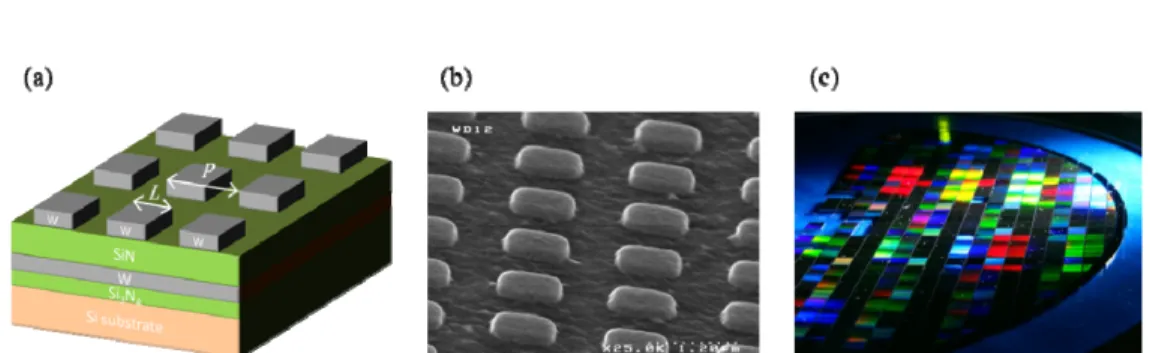
An array of MIM resonators, schematically illustrated on Fig. 1(a), consists of a thin insulator layer sandwiched between a large bottom uniform metallic layer, and top metallic patches. These patches are laid-out on a grid whose pitch must be smaller than the emission wavelength to ensure that no lattice-induced diffraction occurs. The pitch does not influence much the resonance, though, as the MIMs exhibit a plasmonic resonance highly localized below the patches, and thus very few collective effects. This key property will be discussed in more details in the next section. At the interface between the insulating and the metallic layers, surface plasmons can be created, giving birth to a localized Gap Surface Plasmon (GSP) mode. The structure behaves mostly like a metal, thus exhibiting very low emissivity at all but the MIMs resonant frequency. At this frequency, the GSP mode is excited, its enhanced amplitude leading to losses in the metal and to high overall absorption for impinging light. The emission being equal to the absorption as stated by virtue of Kirchhoff’s law, this structure can also be considered as a quasi monochromatic emitter. The important point is to get any parasitic emission (extra resonances or other effects) outside the broad peak of the blackbody spectrum. Overall, the device has to be designed in view of its future use as a membrane to minimize thermal leaks with proper arms to heat it [11], and vacuum encapsulation to suppress air convection as one of the heat leakage channels [12]. However, here, we do not consider the membrane and encapsulation part: we focus on the attainment of the right infrared properties of the MIM array in the CMOS context.
The resonant frequency λr of a MIM is set by the width of the metallic patches L according to the apparently simple formula L = λr/2neff, where neff is the often unusually high effective index of the GSP mode. In this sense, the MIM structure can be seen as a horizontal Fabry-Perot like resonator, where the reflectivity of the GSP mode is obtained at the edges of the metallic patches. In spite of their open nature, the mismatch between the large neff and the outer medium lower index ensures a large (say >70%) GSP modal reflection. The structure can also be seen as a patch antenna. Current on the inner faces are those of the resonant GSP modes, while current near the patch edges are mostly responsible for the coupling [9,10]. In our case, thanks to such a high index neff, a width as small as 800 nm was chosen to target the main absorption peak of carbon dioxide (CO2) at σ = 2350 cm−1 (λ = 4.26 µm). Noting that the thicknesses of the metallic layers play little role in the resonance, it is welcome that the insulator thickness provides a degree of freedom to tune the GSP-air coupling in order to reach maximum absorptivity at resonance (associated to critical coupling) [13]. In our case, we designed the three MIM layers to be 100 nm thick each. As for the period P, we chose P = 1.5 µm. This period keeps the surface plasmon polaritons (SPP) signature gently above the selective absorption line, as will be discussed in detail in the next section.
Given the CMOS compatibility requirement of our devices, we use tungsten (W) as the metal, and silicon nitride (SiN) for the insulator. Noble metals such as gold or silver are well-known to exhibit better plasmonic performances [14], but their use is restricted in a CMOS foundry as they are contaminants for circuitry. Developing a full CMOS-compatible process with conventional lithography is necessary for reducing fabrication costs, and thus make MIMs suitable for industrial applications. The process flow goes as follow: first, a stoichiometric silicon nitride layer is deposited by Low Pressure Chemical Vapour Deposition (LPCVD) at 750°C on the silicon substrate. This layer does not play any optical role, but improves the adherence of the backplane Physical Vapor Deposition (PVD) tungsten layer on top of it. Then the silicon nitride insulator is deposited by Plasma Enhanced Chemical Vapor Deposition (PECVD), and another tungsten layer is deposited once again by PVD. The patches are then defined by deep-UV lithography, and etched by Reactive Ion Etching (RIE). A Scanning Electron Microscope (SEM) image of the patches is displayed on Fig. 1(b). Different variants of MIMs were implemented on the mask, giving the final 200 mm wafer a piecewise iridescent aspect in the visible, as captured on Fig. 1(c).
Fig. 1. (a) Illustration of the MIM structure; (b) Scanning Electron Microscope (SEM) image of the realized resonators; (c) 200 mm silicon wafer with MIMs. Each die is 5 × 5mm2 and consists of a specific kind of MIMs.
3. Results and discussion
The characterisation of the different MIM samples was performed with a Fourier-Transform Infrared (FTIR) Spectrometer (Vertex 70 Bruker). Specular reflectivity was measured with its internal globar IR source and a fitted nitrogen-cooled Mercury-Cadmium-Telluride (MCT) detector, as a function of wavenumber and angle of incidence. The Bruker reflection module was used for that purpose, allowing a focus spot below ~2 mm . Measurements were normalized relative to the reflectivity of a uniform gold sample, which is very close to unity in this mid-infrared frequency region. Emissivity is obtained by
E
= −
1
R
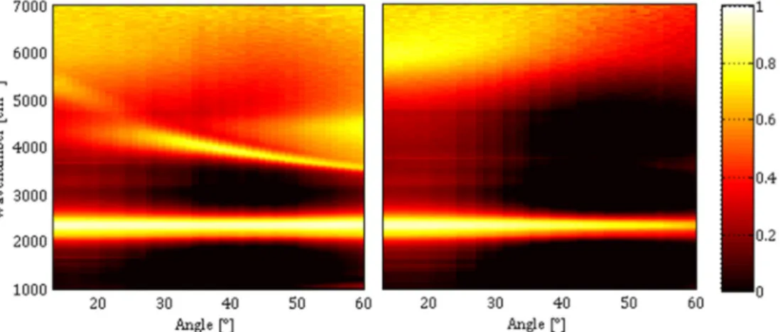
, as the transmittivity of the sample is zero, thanks to the metallic backplane.Figure 2 compares absorption simulations with the full angular characterization of the sample with L = 803 nm patch size along with the related simulation carried out with Rigorous Coupled Wave Analysis (RCWA). The results are displayed between σ = 1000 cm−1 and σ = 7000 cm−1 (λ = 1.43 µm and λ = 10 µm), and for 13° to 60° relative to normal incidence (which is the largest range we can have in our experimental setup). The simulation of Fig. 2(a) concerns the structure as shown in Fig. 1(a), while Fig. 2(b) is a simulation with an added 100 nm SiN protective layer deposited on top of the structure: such a layer will be used for the high-temperature measurement (500°C) described below, it protects tungsten from oxidation. In Fig. 2(a), it is seen that the resonance at σ = 2300 cm−1 is mostly insensitive to the angle, a feature which derives from the localized nature of the GSP resonance of MIM resonators. The weak resonant dispersive and absorptive branch spanning between 3500 cm−1 and 6000 cm−1 corresponds to the propagative surface plasmon polariton (SPP) coupled via the periodicity of the metallic patches. The period of the structure (here P = 1.5 µm) does not change the absorption of the MIM resonance, but contributes to shift this faint SPP dispersion line. In Fig. 2(b), we see that the change induced by the extra SiN layer on top is essentially a spectral shift with negligible broadening for the MIM line, whose frequency is now around 2000 cm−1. We also see that the landscape in the high frequency range changes (3000-6500 cm−1). We are not making an explicit use of this in this paper, but we note that the changed coupling to the outside, at the MIM edges, affects the spectral landscape in this region. Hence, discrepancies that can be seen between Fig. 2(a) (without protective layer) and Fig. 2(c) in this range such as the broad valley of low emissivity near 5000 cm−1 and 30-60° could have their origin in the details of the MIM edges, e.g. in their irregularity.
Fig. 2. (a) Emissivity simulation of L = 803 nm MIM resonators as those of Fig. 1(a), and colorbar on top; (b) same simulation with an extra SiN 100-nm-thick added protective layer; inducing a red shift of the resonance; (c) characterization of realized MIMs. The angular range of this characterization is the one not shaded in (a,b) . Simulations are carried out with RCWA, while characterizations rely on a setup involving an angularly resolved FTIR.
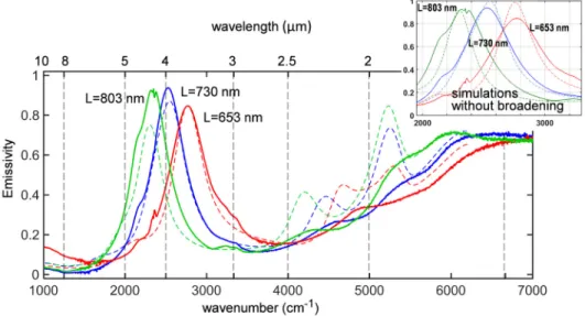
We then checked the influence of the resonators size, by measuring the emissivity of three samples containing MIM with patch sizes of L = 657 nm, L = 730 nm and L = 803 nm. The results are displayed on Fig. 3 alongside corresponding simulations, at 13° from normal incidence. For the simulations, the inset shows that the bare RCWA simulations (inset) are somewhat too narrow and too large, as discussed below. We thus include an empirical Lorentzian-type broadening (convolution) with a [1 + |(ω-ωo)/Γ|m]−1 law with Γ = 80 cm−1 and m = 3 that is less sensitive than a true Lorentzian (m = 2) to adjacent features, to get a very good agreement with the best case (L = 730 nm).
Fig. 3. Measured and simulated MIM spectral emissivities from the reflectivity spectrum at 13° from normal incidence, for three different sizes L of patches as indicated. Solid lines: experimental; dashed lines: simulation with empirical Lorentizan-type broadening included; inset: peak region with non-broadened RCWA simulations (dashed lines).
The resonance is clearly visible between 2000 cm−1 and 3000 cm−1, and redshifts with the increasing size of the patches. This agrees with the GSP resonance trends effectively
described by the abovementioned basic trend L = λr/2neff. Although the resonant frequency is well described by simulation, the experimental amplitude of the resonance is in near perfect agreement for the largest sizes, but clearly below the expectation by ~15% when it comes to the size expected to provide crictical coupling and R~1. This is probably due to imprecisions in the fabrication, which can partially detune the resonators from critical coupling. Furthermore, the tungsten refractive index was taken from Palik’s handbook [15], and may not correspond exactly to that of the tungsten deposited on these samples. This could be a good explanation for the broader peaks, with a Full Width at Half Maximum (FWHM) observed experimentally typically 25% above the expected value. The empirical broadening practiced above takes such possible factors into account. We will see that its interest is to be relevant to the bi-frequency configuration. The rise in emissivity over 4000 cm−1 is caused by the lower reflectivity of the tungsten, which is not as good a metal in this frequency range as noble metals.
Fig. 4. Illustration of a bi-MIM behavior: (a),(b): Simulated magnetic field intensity at resonance inside the insulating layer, for the two resonant frequencies; (c) SEM image of the device, with patches of lengths L1=814nm and L2 =726nm; (d) Comparison of the simulated and measured spectra at 13° from normal incidence (simulation with broadening with the same function as used in Fig. 3, showing the same degree of smearing as experimental data).. Inset:same spectra as the main figure, with an added dash-dotted line showing in addition the non broadened spectrum, with the two peaks related to the two mode patterns (a,b).
From this successful achievement of monochromatic CMOS-compatible MIM emitters, we took advantage of the large absorption cross-section of the MIM to develop bispectral structures [8, 16, 17]. For NDIR applications, it is often relevant to use a reference
measurement in order to overcome variations due to temperature, humidity, or aging of the source. This additional measurement cannot be taken through a CO2-free reference gas cell. Instead, it is taken at a nearby wavelength where no absorption occurs for the gas in consideration. It is thus essential to be able to design sources emitting a two different wavelengths of modest separation. Figure 4. illustrates the results obtained for a structure designed to emit simultaneously at σ = 2300 cm−1 and σ = 2560 cm−1. The structure consists of two patches with different sizes lengths L1=814 nm and L2 =726 nm set in a staggered arrangement on a square grid of period P 2.26 m= µ . Each patch then absorbs a specific frequency.
Although the two absorption peaks are not fully merged in simulation without empirical broadening (shown in inset of Fig. 4(d), same parameter as Fig. 4), they tend to merge substantially in the experiment, a trend that we ascribe mostly to the lower quality factor of the resonances, combined with a ~20% difference in peak amplitude. We remark that the broadened version of Fig. 4(d) displays the right degree of smearing of the peak as the experimental data, with an almost flat top in the simulation, while it is an almost straight and tilted line due to the imbalance of the two peaks in the experiment. However, light is still emitted at these two frequencies, thus validating the possibility of implementing a reference channel with this kind of nanostructuration. The large absorption cross section of MIMs, typically an order of magnitude larger than their physical area, allows two different MIMs organized in matrix to totally absorb the incident light at their respective resonant wavelength, although they each cover approximately half of the substrate surface, which can be seen as spectral sorting.
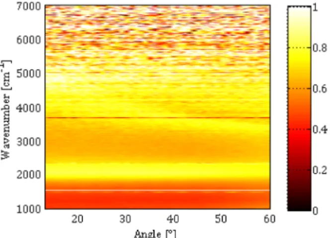
The invariance of the structure by 90° rotation ensures that the emission is identical in both TE and TM polarization. This was verified experimentally by adding a polarizer on the optical path between the source and the sample. The results are presented on Fig. 5 for patches of length L = 803nm. The gold reference was also measured for the sole TE or TM polarization, which is why the emissivities reach 100% instead of the expected 50%. The real emissivity is the average of the plotted polarized emissivities.
Fig. 5. MIMs emissivity characterization in TM (left) and TE (right) polarization using a polarizer on the optical path of the FTIR.
The only noticeable difference between the two polarizations is the presence of the propagative SPP dispersion curve in the TM spectrum, since only the TM’s vertical field component excites the SPP. The selective GSP resonance is thus polarization-independent, granting maximum optical flux at the resonant frequency when this structure is used as an emitter. Polarization effects are more extensively discussed in [9,18], for example.
Finally, the MIM emissivity was directly measured by heating the sample at 500°C, now using it directly as an external source for the FTIR spectrometer. A 100 nm thick silicon nitride layer was added on top of the previous stack to prevent the tungsten premature oxidation. This has been seen in Fig. 2 to induce a substantial redshift, and some extra broadening as well. The measured emissivity is presented on Fig. 6.
Fig. 6. Direct measurement of the emissivity using the L = 803 nm heated sample as an external source for the FTIR.
Although the measurement is quite noisy at high frequencies due to the very low amount of photons collected, the resonance can still be observed around 2100 cm−1, a bit lower than the 2300 cm−1 measured beforehand. This redshift was clarified by taking into account in simulation the additional silicon nitride layer on top of the structure, which in the simplest view increases the effective index of the resonant mode (the phase shift upon reflection may also be affected). The low contrast is attributed to the very small size of the sample (5 × 5 mm2), which makes it difficult to image only the sample. Hence a fraction of the heater around it is likely to contribute to the background. Nevertheless, this measurement confirms that these CMOS-compatible structures do act as spectrally selective emitters at typical useful temperatures (an optimized nitride coating should allow us to heat the emitters up to 700°C).
4. Conclusion
In this work, we have outlined the conception and realisation of spectrally selective MIM structures, in a CMOS compatible foundry on 200 mm Si wafers, in areas large enough to behave as thermal emitters of sizable absolute irradiance at their emission peak, here the CO2 absorption band λ = 4.26 µm. The samples were characterized using an angularly resolved FTIR spectrometer, showing a lithographically tunable resonance, with the expected angle- and polarization-independent feature. The possibility to design bi-spectral structures is also a key element in order to achieve efficient integrated sensors with an included reference channel. These results are promising in the prospect of using these sources on MEMS-like emitters in order to increase the efficiency of NDIR gas sensors. The next step is to directly integrate these structures on suspended microhotplates, using the Joule effect in tungsten or in another underlying metal layer to heat them to their working temperature.