HAL Id: hal-01715882
https://hal.archives-ouvertes.fr/hal-01715882
Submitted on 16 Mar 2018
HAL is a multi-disciplinary open access
archive for the deposit and dissemination of
sci-entific research documents, whether they are
pub-lished or not. The documents may come from
teaching and research institutions in France or
abroad, or from public or private research centers.
L’archive ouverte pluridisciplinaire HAL, est
destinée au dépôt et à la diffusion de documents
scientifiques de niveau recherche, publiés ou non,
émanant des établissements d’enseignement et de
recherche français ou étrangers, des laboratoires
publics ou privés.
Observation and manipulation of
tris(dibenzoylmethanato)ruthenium molecules by low
temperature scanning tunnelling microscopy
Loranne Vernisse, Olivier Guillermet, Jacques Bonvoisin, Roland Coratger
To cite this version:
Loranne Vernisse, Olivier Guillermet, Jacques Bonvoisin, Roland Coratger. Observation and
manip-ulation of tris(dibenzoylmethanato)ruthenium molecules by low temperature scanning tunnelling
mi-croscopy. Surface Science, Elsevier, 2014, 619, pp.98-104. �10.1016/j.susc.2013.09.017�. �hal-01715882�
low temperature scanning tunneling microscopy
L. Vernisse, O. Guillermet, J. Bonvoisin, and R. Coratger
CEMES, CNRS UPR 8011 et Universit´e Paul Sabatier, 29 rue J. Marvig, BP 94347, F-31055 Toulouse, France∗
(Dated: September 24, 2013)
The behaviour of tris(dibenzoylmethanato)ruthenium molecules has been studied using low tem-perature scanning tunneling microscopy after adsorption on Ag(111) and Cu(111). On both surfaces, the molecules present two adsorption geometries : a bi-lobed and a chiral threefold structure. This latter form can stand up to adopt a bi-lobed conformation which is oriented along the dense crys-tallographic directions. The molecular geometries after adsorption can be modified using the STM tip. In one of these modifications, a switch between two different conformations has been observed. The data recorded during the experiments show that this phenomenon is induced by the electric field in the STM junction.
Keywords: Scanning tunneling microscopy, UHV, low temperature, adsorption, ruthenium complexes, switch
I. INTRODUCTION
In molecular electronics, charge transfer in single molecules is of fundamental importance in the building of future active components [1]. Accordingly, a great number of investigations deals with the properties of molecules adsorbed on flat surfaces which can be used for this purpose. This interest is due to the fact that the behaviour of these molecules can be substantially changed when they are deposited on a substrate as com-pared to the properties observed in the gas phase. In-deed, the interactions with the surface significantly dis-rupts their electronic states which then couple each other [2, 3]. Among these molecules, only a few examples deal with the study of mixed valence complexes [4, 5]. These molecules are of peculiar interest since charge transfer between the redox centres offers the opportunity to per-form charge engineering at the molecular scale. In this context, it is important to characterize single molecules since most of the usual characterisation techniques aver-age their physical and chemical properties. This explains that in the recent years, scanning tunneling microscopy (STM) and its amazing resolution has largely been used to investigate a wide variety of molecules. These latter are then deposited on metal surfaces [6], semiconduct-ing substrates [7, 8] or ultra-thin insulatsemiconduct-ing layers [9] from crucibles or more simply from filaments heated by Joule effect. These constraints imply that the molecules should be able to support ultra high vacuum (UHV) con-ditions, evaporation process and adsorption on the sub-strate without any perturbations [10]. Then, their sta-bility appears as a key point for in depth STM investiga-tions. These conditions are generally fulfilled for planar molecules [11] but the situation is more complex for large 3D compounds which is generally the case for mixed va-lence complexes.
∗vernisse@cemes.fr
Another point concerns the ability of these molecules to exhibit different switching states, characterized by different chemical and/or physical properties [12]. For mixed valence complexes, this is particularly important since the different oxidation states are linked to charge transfer through the molecule. In STM experiments, the switch is generally due to inelastic electrons tunneling through the junction [13, 14]. One of the most striking examples concerns azobenzene derivatives adsorbed on noble Au(111) surfaces which can be switched between the cis and trans isomers as a function of tunneling cur-rent [14]. More rarely, the field generated by the applied bias voltage leads to conformational changes [15]. For molecular landers, these changes allow to manipulate the molecule on the surface because the electrical field in-duces a dipole in the molecular legs [16]. The molecular charge in mixed valence moieties is generally induced by sudden bias voltage variations [17] and then, one has to anticipate the possible resulting conformations. Thus, in accordance with the two points discussed above, mixed valence complexes should be first, easily deposited and then, manipulated with the tip if one is interested by their different charging states after adsorption.
In previous papers, we reported the first STM char-acterization of mononuclear ruthenium complexes with different ligands [18, 19]. These molecules are of pecu-liar interest in the route towards the synthesis of larger entities devoted to charge transfer. We also showed that their evaporation on Ag(111) resulted in two different ad-sorption geometries, bi-lobed and threefold objects, the latter presenting two chiral structures.
In this article, we have particularly studied tip-dependant modifications of the molecular geometry after adsorption of tris(dibenzoylmethanato)ruthenium (Ru(dbm)3) on Ag(111) and Cu(111). On the two
sub-strates, the adsorption geometries are the same. A first set of manipulations shows the transformation of a three-fold object to a bi-lobed conformation. It is also demon-strated that the bi-lobed structure presents an unex-pected property which consists in a switch between two
2 different conformations controlled using the STM tip.
FIG. 1. Chemical structure of the Ru(dbm)3 molecule.
Car-bon atoms are in grey, hydrogen in white, oxygen in red. The central blue atom is ruthenium.
II. EXPERIMENTAL DETAILS
Scanning tunneling and atomic force microscopy exper-iments have been performed at liquid helium temperature (T = 4, 5 K) on a commercial STM-AFM (LT Omicron) working with a base pressure of 2× 10⁻¹¹ mbar. The Ag(111) and Cu(111) crystals are cleaned by repeated Ar+ bombardment cycles at E = 600 eV followed by
an-nealing at 800 K for one hour. The Ru(dbm)3 molecule
(Fig 1) is a three-dimensional object containing 85 atoms. The molecules are deposited on a W filament 0.15 mm in diameter. This filament is submitted to high temperature outgassing cycles before evaporation. In these manipu-lations, the substrate was held at liquid helium temper-ature and the molecules are directly evaporated on the STM head through a small hole 4 mm in diameter drilled in one of the windows of the He cryostat. The filament temperature is estimated to be∼250◦C. The small dis-tance between the filament and the surface supports very small evaporation rates with typical values in the 1/1000 monolayer range. These conditions are used for single molecule experiments in which the thermal diffusion is inhibited. STM tips made of tungsten wires 0.25 mm in diameter were prepared by electrochemical etching in ambient conditions and substantially cleaned in UHV us-ing direct current heatus-ing. Bias voltage is applied to the sample. The tuning fork tips used in NC-AFM/STM were made of platinum-iridium wires 0.05 mm in diam-eter cut by focused ion beam. The images have been presented using the WSXM software [20].
III. RESULTS
A. Details of the adsorption geometry
Large scale STM images of the Ag(111) and the Cu(111) surfaces after Ru(dbm)3 evaporation are shown
in Figs. 2a and b. These images show that the two differ-ent objects already described in [18] on Ag(111) are the same on Cu(111). The most common structure consists in a two lobed entity (called type B) with an apparent height of about 4 ˚A (insert in Fig 3).
FIG. 2. STM image 75× 75 nm2 of the Ru(dbm)3molecules
after evaporation on (a) the Ag(111) and (b) Cu(111) sub-strate held at low temperature (Vs = −1 V, It = 1 pA,
T = 4.5 K).
FIG. 3. Orientation of the bi-lobed structure on Cu(111). The orientation of the top ligand of most of the molecules are represented with white lines. Insert : Close up view (5× 5 nm2) of the bi-lobe structure called B. (Vs = 1.5 V, It =
15 pA, T = 4.5 K)
The orientation of these bi-lobed structures with re-spect to the underlying structure is not randomly
dis-tributed. To show this effect, white lines have been drawn in Fig. 3 along the direction of the bi-lobed shape molecules. We noticed that these lines are oriented along the three crystallographic [110] type directions of the sample. This observation is confirmed by the distance between two lines, which is always a multiple of the Cu lattice parameter, for example in Fig 3. This observation is also supported by the orientation of the molecule in the calculated images described in [18]. The same results are observed on the Ag(111) surface, which has a different lattice parameter than the Cu(111). This confirms that this effect is not due to the substrate but is an effect of the adsorption of the dbm ligands themselves along close packed directions.
The second type of object can be described as a three-fold structure (called type T ) presenting a lower apparent height of about 3 ˚A. Details of this structure are pre-sented in Fig. 4 where small scale images performed on two of these objects are shown. These objects present two different orientations once adsorbed on the surface since the rotation of their peripheral groups is anticlockwise (Fig. 4a) or clockwise (Fig. 4b). Among the T structures, the right and left handed configurations are equally dis-tributed on the surface. Note also that this geometry and the resulting chirality is the same whatever the substrate.
FIG. 4. Close up view (3.6× 3.6 nm2) of the second
three-fold structures called T type showing two eniantomers of the structure (Vs= 1.5 V, It= 15 pA, T = 4.5 K).
The images presented so far show that the molecule adsorbs in two different ways on the surface. These re-sults have been confirmed by molecular mechanics cal-culations in which the type B geometry corresponds to two dbm groups parallel to the surface and the T type to three phenyl groups forming an octahedral struc-ture [18]. Therefore, the bi-lobed strucstruc-ture can be assim-ilated to a standing up form and the threefold structure to a laying down one. For clarity, these two forms are sketched in Fig. 5. Statistics show that the ratio is about
B/T = 80/20 between the two structures present on the
surface, whatever the substrate, Ag(111) or Cu(111).
B. STM manipulation
To confirm that the two forms are produced by the same molecule, we show that it is possible to change its adsorption geometry or its appearance using the STM tip. Such manipulations are nevertheless tightly
depen-FIG. 5. Schema of the two adsorption geometries on the sur-face. The corresponding structure is added. a) Bi-lobed (B) and b) threefold (T) form
dant on the tip shape. Details of these experiments are presented below.
1. Adsorption geometry modification
The first observed manipulation consists in ”picking up” a threefold object (type T ) in order to produce a bi-lobed conformation (type B). An example of this ex-periment is presented Fig.6.
FIG. 6. STM images 15× 15 nm2conducted during the mod-ification of a type T in a type B structure: a) before manipu-lation 1 (dashed white circle), b) after manipumanipu-lation 1 (white circle) and before manipulation 2 (blue dashed circle) and c) after modification 2 (full blue circle) (Vt= 1.5 V, It= 15 pA,
T = 4.5 K).
Fig. 6a shows a type B and two type T molecules. In a first step, the tip is placed above the white dash circled molecule (1). Next, the bias voltage is increased to a value of 2.5 V, while the feedback loop maintains the tunneling current constant. This induces a sudden change in the molecular adsorption geometry to the bi-lobed conformation (B type) as seen in the white circle of Fig. 6b. The same procedure can be applied to the second T molecule (blue dashed circle ). The tip is placed again above the considered molecule (2). After the rise of the bias voltage to 2.5 V, the molecule geometry changes again to a type B geometry (full blue circle in Fig. 6c). This process is reproducible only if the tip has a rather blunt shape. This phenomenon can be explained by a large area in the tip sample junction in which a high electric field is applied. By the way, the electrostatic force due to the presence of the electric field has an effect on the whole molecule, which induces a modification of the adsorption geometry instead of breaking bonds [21]. On
4 the other hand, it is impossible to change the chirality
of a T object whatever the sign and value of the applied voltage.
It is also impossible to obtain a threefold object (T type) from a B form object. This is explained by the flat adsorption of two dbm moieties on the surface, which induces the formation of a very stable structure on the substrate. The last dbm points upward and has a larger degree of freedom. In this case, the high electric field breaks the chemical bonds instead of desorb the two other ligands. As a consequence, the molecule cannot lay down and does not exhibit a T type geometry.
2. Switch manipulation
Following the experiments reported before, it has been observed than sharper the tip, more unstable become the molecules when the bias voltage exceeds +2 V. This phe-nomenon is only observed on type B molecules. Indeed, when a sharp tip is placed above a bi-lobed molecule and the bias voltage is raised up to about 2.1 V, a slight change of the B conformation is observed. The result of this manipulation is presented in Fig. 7a.
FIG. 7. a) STM image of a modified type B molecule called ”state 1” [The two marks on the molecule are discussed in the text] b) NC-AFM image of the same molecule in constant height mode (4× 4 nm2, and Vt = 200 mV, Amplitude = 100 pm, T = 4.5 K) c) STM image of a modified type B molecule called ”state 2”.
This image shows that the bi-lobe structure is still vis-ible but with smaller lobes. Indeed, the apparent height only reaches 2.6 ˚A against 3.8 ˚A before the experiment. The square shape of the base made of two dbm is thus highlighted. This peculiar geometry called ”state 1” in the following was investigated by non-contact AFM. As seen in Fig 7b, the NC-AFM image performed at con-stant height shows two cycles with four sides. It has been shown that the NC-AFM contrast strongly depends on the tip sample distance [22] and only the parts of the molecule within the same range of distance to the tip are resolved. Due to the three-dimensional geometry of the molecule and possible deformation of phenyl rings around the Ru center due to the electrical field, the up-ward dbm ligand is tilted with respect to the vertical. Note that such a NC-AFM contrast is never observed on unperturbed molecules since their upper dbm ligands al-ways point strictly vertically. This two four sides cycles are therefore attributed to four of the six C-C bonds of
the dbm ligand pointing upwards, the two others being closer to the Ru center. In addition, the ring diameter corresponds to the theoretical value. This image mostly shows that the molecule retains its structure after the bias voltage increases.
In the same experimental conditions, a second geom-etry is also observed. The top bi-lobe structure has ro-tated about 30◦ and appears to be oriented along the side of the square base instead along the diagonal. This second geometry is called ”state 2” and is presented in Fig.7c.
The modification of the bi-lobed form can be per-formed on the Ag(111) or Cu(111) surfaces if the tip is sharper enough. In addition, a switch between the two states can be observed. When the tip is located above one of the molecule lobes, the tip-surface distance varia-tions can be recorded as a function of time, the tunneling current being kept constant. At low polarisation, the z tip position does not change, which means the molecule remains in its original state. When the bias voltage ex-ceeds the threshold value of +2.1 V, the switch between the states 1 and 2 takes place, resulting in sudden jumps in the tip height.
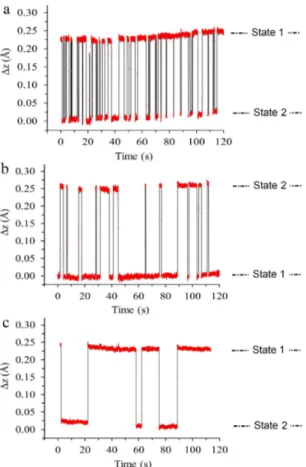
Figs. 8a and 8b illustrate this phenomenon. These curves conducted over several minutes at a bias volt-age of 2.2 V show that the tip height is time dependent and presents two distinct levels. In a first experiment (Fig. 8a), a bias voltage of 2.2 V is applied on the bot-tom lobe in the state 1 (black circle in Fig. 7a). Then, the bi-lobed structure evolves to the state 2 (Fig 7c). The lobe is then out of the tip. As a consequence, state 1 corresponds to the high level of the graph, since state 2 corresponds to the low level. A calculation of the aver-age residing time on each state shows the tip stays about 2.52± 0.02 seconds in state 1 and 1.32 ± 0.02 seconds in state 2. In a second experiment (Fig. 8b), the tip is placed above the blue circle of Fig. 7a. The tip height switches between state 1 where it is above the square base (low level) and state 2 where it is above a lobe of the bi-lobed structure (high level). The residing times are 1.7± 0.02 sec in state 2 and 5.6 ± 0.02 sec in state 1 respectively. The molecule preferentially adopts the low level state and then, the geometry presented in Fig. 7a. In both cases, the height variation is about 0.25 ˚A and corresponds to the rotation of the upper dbm under the tip.
The life time of each state is random but the number of switches as a function of time depends on the bias voltage. To show this dependence, the tip is again located above the blue circle of Fig. 7a but a bias voltage of 2.1 V is applied. Fig. 8c shows the variations of the tip height as a time function. The curve exhibits the same two steps shape but the time length of each state is longer than for an applied voltage of 2.2 V. This value is about 20.25± 0.02 sec for the high level state against 9.15 ± 0.02 sec for the low level state. Therefore, the molecular conformations are more stable than at 2.2 V, especially state 1. This can be explain by the low electrical field,
FIG. 8. Variations of the tip height as a function of time over a type B structure at a bias voltage of 2.2 V while the tip is positioned above a) the black circle, b) the blue circle in Fig 7a. c) Variations of the tip height as a function of time at a bias voltage of 2.1 V while the tip is positioned above the black circle. These data have been extracted from a more complete data set recorded during 6 mn.
which can engage the switch but is not high enough to increase the transition rate. This phenomenon occurs for a very small bias range (from 2.1 V to 2.2 V since at 2.3 V the molecule is damaged) and does not depend on the tunneling current.
Using the variations of the tip height as a function of time, it is then possible to block with a high reproducibil-ity the molecular configuration in its initial state (state 1 and initial state after adsorption) or in a new confor-mation (state 2). For this, the bias voltage is decreased below 2 V while the tip is on the chosen state. The tip scan is thus resumed and a new image is recorded to confirm the result of the manipulation.
IV. DISCUSSION
Most of the experiments performed so far on mixed va-lence complexes deal with the observation of di-nuclear complexes deposited on metallic surfaces at relative high coverage [4, 5]. The molecular interactions within the
layer generally led to the formation of more or less self assembled domains in which the characterization of single molecules was rather difficult. However, the study of sin-gle moieties which can be further used to construct large molecules, appears fundamental. From this point of view, our experiments demonstrate that the Ru(dbm)3
com-plex can be easily evaporated using a standard technique to obtain isolated molecules on a metallic surface. The role of the dbm ligand is particularly interesting since it allows evaporation and adsorption on the surface with-out any damage to the molecule. This interest is also enhanced when one considers the two adsorption geome-tries of Ru(dbm)3. The capacity to access a bi-lobed
form from a threefold geometry thanks to the STM tip shows these two configurations come from the same entire molecule and not a damaged one.
This particular property of dbm ligands is first under-lined by the higher stability of the B form, where two dbm are lying flat on the substrate. Indeed, the adsorp-tion energy of this latter was found to be 0.60 eV, while the T form only reaches 0.34 eV on Ag(111) [18]. Thus, about 80% of the observed molecules present the B form after adsorption. Moreover, these objects are oriented af-ter adsorption along the three crystallographic [110] type directions of the sample. The same results observed on both Cu(111) and Ag(111) surfaces, which have differ-ent lattice parameters, confirm that this is due to the flat adsorption of the two dbm ligands on the substrate along close packed directions. In addition, it has been shown that a T form can be irreversibly ”picked up” in order to produce a bi-lobed geometry. The irreversibility of the process, i.e. the impossibility to produce a T form from a bi-lobed geometry, confirms the higher stability of the molecule when the dbm ligands are adsorbed flat on the surface. All theses observations also suggest that the bi-lobe conformation will be more sensitive to the elec-trostatic field produced by the STM tip because of the dbm ligands pointing upwards. This sensitivity largely explains the presence of a molecular switch.
A molecular switch implies a reversible transformation between at least two distinct stable switching states, usu-ally geometrical or valence isomers [23–26]. For example, M. Lastapis et al. selectively activated different reversible movements of an individual biphenyl molecule adsorbed on a Si(100) surface due to the application of a nega-tive voltage of about -3 V [27]. Similarly, L. Grill et al. observed the isomerization of azobenzene [28]. They showed that azobenzene adopts two different geometrical conformations: a planar (trans) and a non planar three-dimensional (cis) form. The reversible switch is engaged by voltage pulses of about 6 V above a molecular island. Specific intra-molecular conformations or peculiar molec-ular adsorption geometries can also be achieved on a sur-face while they would not be present after evaporation, because they are energetically not favoured [29, 30]. Gen-erally, these experiments are performed on small and/or flat molecules. These latter are easily manipulated or are particularly sensitive to the electric field locally produced
6 by the STM tip to switch between different molecular
states. For large bulky objects, these experiments are more difficult to perform and suffer from a lack of repro-ducibility. This can be partly explained by the relative fragility of such large structures.
Then, the ability to observe a reproducible switch on the Ru(dbm)3 molecule is particularly interesting. As
said before, only the two lobed structure exhibits this characteristic, this adsorption geometry being particu-larly suited for this manipulation. The results show that a first step is yet required to engage the switching process. This involves applying a bias voltage above +2 V above the molecule during a couple of seconds. A slight mod-ification of the molecular appearance is then observed. The molecule reaches an ”intermediate state” where the two lobes become slightly asymmetric and present a lower corrugation.
In this intermediate state, the ruthenium complex ex-hibits two distinct switching conformations which are voltage dependant: a square base adsorbed on the Ag(111) surface and a bi lobe structure pointing upwards with two distinct orientations (Fig.8). To switch between these two conformations, the tip is fixed above one of the two lobes and the positive bias voltage is increased (with a maximal value of +2.2 V). We noticed the molecule is stable at negative voltages down to -3.5 V and the switch appears only for positive voltage from +2.1 V (applied bias voltages below -3.5 V or above 2.2 V destroy the molecule) Moreover, if the bias voltage is fixed just be-low the switch threshold and if the applied current is increased until 70 pA (which is more than 10 times the initial value), the intermediate state is still stable. The only way to engage the molecular switch is to increase the bias voltage above 2 V, independently of the current used. The switching rate only depends on the voltage value and not on the tunneling current (Figs. 8c and d.). This confirms that no inelastic effect comes into play in this process. The bias voltage range is rather small (from 2.1 to 2.2 V), so that a statistical analysis is difficult to achieve. However, the different residing times shows that the state 1 is more stable.
The tip shape is also important to perform a given ma-nipulation. If the tip is fine enough, these two conforma-tions can switch in a controlled and reversible way. The modification is therefore closely linked to the localisation area of the electric field under the tip [31, 32]. Using a simple geometrical model of Coelho and Debeau [33], it is possible to calculate the lateral extension of the elec-trical field between a plane and an hyperbolic tip. Given the tunnelling currents and bias voltages used in these experiments, the tip-to-sample distance is estimated to be d≈1 nm. Thus, a tip curvature radius of 8 ˚A implies that the area around the tip apex in which the field is between Emax= Vt/d and 75 % of Emaxcorresponds to
the size of the molecule (diameter of 1.48 nm, Fig. 1). This area is more than 3 times larger (6.2 nm2) when the curvature radius is only 12 ˚A. Then, the tip has to be terminated by a single atom to perform the switch
ex-periments on the B state (the field is located on a precise point of the molecule). For a blunt tip made of an atomic cluster fixed on a macroscopic base, the lateral extension of the field is used to manipulate the whole T molecule to produce a B structure or to cause eventually a lateral displacement of this latter. As a consequence, the B form does not evolve to the intermediate state and no switch is observed.
The switching from T to B type occurs at a bias voltage of 2.5 V, i.e. a value higher than the threshold for disso-ciation of a B molecule (2.3 V). This difference can also be explained by an effect of the electric field in the STM junction. On T objects, the corrugation is about 3 ˚A and the adsorption geometry is relatively flat (three dbm ly-ing on the surface, Fig. 5b). For B type molecules, the apparent height is 4 ˚A but a dbm group points upwards. The first adsorption calculations show that the two struc-tures present a height difference of about 2.5 ˚A [18]. This implies that the molecule-tip distance is larger on a T type than on a B structure, resulting in a lower electric field. A T type molecule is then able to switch in a B type at 2.5 V while a B type would be dissociated at the same voltage.
Another point to consider is the irreversibility of the process. Indeed, the switched molecule never returns to the original bi-lobed shape presenting the highest corrugation, whatever the value and sign of the applied bias voltage (this latter being smaller than 2.3 V to avoid fragmentation). A first hypothesis suggests that the applied bias voltage could give to the molecule enough energy to adopt a new adsorption geometry as the substrate is held at 4 K during evaporation. From this point of view, Ru(dbm)3 are relatively fragile as
compared to planar molecules which can be imaged at voltages above 3 V without any problem. Then, the change in geometry is probably not sufficient to explain the irreversibility of the switching process. It was then assumed that the first step necessary to allow the switch is accompanied by a modification of the oxidation degree of the Ru atom. Indeed, this atom can change its oxidation state from Ru(III) to Ru(II) due to electron injection induced by the STM tip. This effect has already been observed on Cu complexes. Indeed, Leoni et al. reported the switching behaviour of a Cu(dbm)2
complex where the transition between a square planar and a 3D tetrahedral geometry was due to the transition between the Cu(II) and Cu(I) oxidation states [30]. However, as opposed to our experimental results, their process is perfectly reversible. In the Ru(dbm)3 case, it
is unlikely that the negative charge irreversibly remains on the ruthenium, which discards this hypothesis.
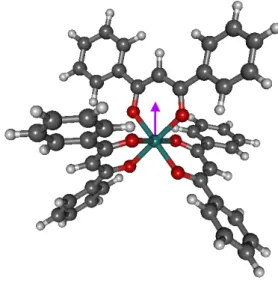
As explained before, the process is driven by the elec-tric field in the STM junction. The electric field can induce deformation for permanently charged atom or molecules [34]. It can also interact with dipolar moments of certain molecules [16]. The Ru(III) ion exhibits an octahedral low spin d5 configuration. The degenerate
FIG. 9. Structure obtained by DFT calculations in gaz phase showing the dipole moment orientation (purple arrow). A value of 0.98 D has been obtained.
ground-state leads to a break in degeneracy which stabi-lizes the molecule and reduces its symmetry according to the Jahn-Teller effect [35]. In a previous paper (supple-mentary data in [18]), it was noticed that two Ru-O bond lengths in the Ru(dbm)3 compound are slightly longer
than the four others (about 0.03 ˚A). A dipole moment of 0.98 D has been also calculated for the compound in gas phase using DFT calculations [36]. As seen in Fig 9, this dipole moment takes place between the Ru atom and one of the dbm.
After adsorption, the B type molecule is even more distorted due to the interaction with the surface and its dipole moment should increase. Moreover, the AFM im-age shows that in the intermediate state, the upper dbm ligand is tilted compared to the original bi-lobed shape (Fig.7b). This also involves a tilt of the dipole moment. If this moment is not collinear to the electric field cre-ated by the tip, the state becomes unstable and sets off a rotational movement of the upper lobe limited by the steric hindrance within the molecule. The rotation of the whole upper dbm ligand can be also accompanied by a small rotation of each phenyl group. Indeed, the rotation of these later requires only a few tenths of eV [37].
Sim-ple molecular dynamics calculations demonstrate that a rotation of about 20 degrees of the upper dbm moiety is possible. This movement also includes a small rotation of the two phenyls of a few degrees in good agreement with the hypothesis previously discussed and with the NC-AFM observations. The effect of the electrical field on the molecular dipole moment is linked to the presence of the so-called intermediate state which in turn implies a molecular structure modification. It is assumed that this intermediate state is related to the dissociation of one of the top C-H bonds of the molecule. Controlled break-ing of C-H bonds have already been conducted usbreak-ing an STM tip [38, 39]. Particularly, Ho et al. have broken C-H bonds on different molecules and observed that the H atom was imaged such as a small depression on a cop-per surface. This is good agreement with the small de-pression observed in the molecule center in state 2. The dehydrogenation can also explain that the bi-lobed ge-ometry needs a positive voltage and a sharp tip to access the ”intermediate state” and is also consistent with the irreversibility of the phenomenon.
V. SUMMARY
It has been observed that tris(dibenzoyl-methanato)ruthenium complex adsorbs in two different ways on Ag(111) and Cu(111) surfaces: a bi-lobed and a chiral threefold structure. We have shown that the threefold structure can stand up to adopt a bi-lobed conformation, in which the upper ligand and then, all the molecule is oriented along a dense crystallographic direction. This last structure can irreversibly adopt a new conformation which is able to switch between two geometries. The switch itself is caused by an applied bias voltage from 2.1 V. These results are consistent with a first dehydrogenation of the molecule followed by a tilted dipole moment sensitive to the local electrical field produced by the tip. Calculations are in hand to solve the very interesting but also complex phenomenon. Finally, the results show that it is possible to manipulate large 3D objects, which is very promising for future molecular electronic devices made of mixed valence complexes with several ruthenium centers.
[1] C. Joachim, J. K. Gimzewski, A. Aviram Nature 408 (2000) 541.
[2] N. Koch, S. Duhm, J. P. Rabe Phys. Rev. Lett. 95 (2005) 237601.
[3] F. Jackel, U. G. E. Perera, V. Iancu, K. F. Braun, N. Koch, J. P. Rabe, S. W. Hla, Phys. Rev. Lett. 100 (2008) 126102.
[4] Y. Lu, R. C. Quardokus, C. S. Lent, F. Justaud, C. Lap-inte, S. A. Kandel, J. Am. Chem. Soc. 132 (2010) 13519.
[5] R. C. Quardokus, Y. Lu, N. A. Wasio, C.S. Lent, F. Justaud, C. Lapinte, S.A. Kandel, J. Am. Chem. Soc.
134 (2012) 1710.
[6] J.V. Barth, Ann. Rev. Phys. Chem. 58 (2007) 375. [7] Ch. Nacci, J. Lagoute, X. Liu, S. F¨olsch, Appl. Phys. A
93 (2008) 313.
[8] S. Info, Y. Cao, K.S. Yong, Z.Q. Wang, W.S. Chin, Y.H. Lai, J.F. Deng, G.Q. Xu, J. Am. Chem. Soc. 122 (2000) 1812.
8
[9] J. Repp, G. Meyer, S.M. Stojkovic, A. Gourdon, C. Joachim, Phys. Rev. Lett. 94 (2005) 26803.
[10] S.E. Grillo, H. Tang, C. Coudret, S. Gauthier, Chem.
Phys. Lett. 355 (2002) 289.
[11] B. Calmettes, S. Nagarajan, A. Gourdon, M. Abel, L. Porte, R. Coratger, Angew. Chem. Int. 47 (2008) 6994. [12] S.J. van der Molen, P. Liljeroth, J. Phys. Condens.
Mat-ter 22 (2010) 133001.
[13] P. Liljeroth, J. Repp, G. Meyer, Science 317 (2007) 1203. [14] M. Alemani, S. Selvanathan, F. Ample, M. V. Peters, K.H. Rieder, F. Moresco, C. Joachim, S. Hecht, L. Grill,
J. Phys. Chem. C 112 (2008) 10509.
[15] C. Girard, C. Joachim, C. Chavy, P. Sautet, Surf. Sci.
282 (1993) 400.
[16] L. Grill, K.H. Rieder, F. Moresco, S. Stojkovic, A. Gour-don, C. Joachim, Nano Lett. 6 (2006) 2685.
[17] Y.L. Huang, Y. Lu, H. Huang, S. Kera, N. Ueno, W. Chen, Small 8 (2012) 1423.
[18] S. Munery, N. Ratel-Ramond, Y. Benjalal, L. Vernisse, O. Guillermet, X. Bouju, R. Coratger, J. Bonvoisin, Eur.
J. Inorg. Chem. 17 (2011) 2698.
[19] L. Vernisse, S. Munery, N. Ratel-Ramond, Y. Benjalal, O. Guillermet, X. Bouju, R. Coratger, J. Bonvoisin, J.
Phys. Chem. C 116 (2012) 13715.
[20] I. Horcas, R. Fernandez, J. M. Gomez-Rodriguez, J. Gomez-Herrero, A. M. Baro, Rev. Sci. Instrum. 78 (2007) 013705.
[21] C. Chapman and I. Paci, J. Phys. Chem. C 114 (2010) 20556.
[22] L. Gross, F. Mohn, N. Moll, P. Liljeroth, G.Meyer,
Sci-ence 325 (2009) 1110.
[23] S. Hla, JVST B 23(4) (2004) 1351.
[24] N. Lorente, R. Rurali, H. Tang, J. Phys.: Condens.
Mat-ter 17 (13) (2005) 1049.
[25] F. Moresco, G. Meyer, K.-H. Rieder, H. Tang, A. Gour-don, C. Joachim, Phys. Rev. Lett. 86 (2001) 672. [26] B.-Y. Choi, S.-J. Kahng, S. Kim, H. Kim, H. W. Kim,
Y. J. Song, J. Ihm, Y. Kuk, Phys. Rev. Lett. 96 (2006) 156106.
[27] M. Lastapis, M. Martin, D. Riedel, L. Hellner, G. Comtet, G. Dujardin, Science 5724 (2005) 1000. [28] M. Alemani, M. V. Peters, S. Hecht, K.-H. Rieder, F.
Moresco, L. Grill, J. Am. Chem. Soc. 128, (2006) 14446. [29] B. L. Ferringa, Molecular Switches (Wiley-VCH,
Wein-heim, 2001)
[30] T. Leoni, O. Guillermet, H. Walch, V. Langlais, A. Scheuermann, J. Bonvoisin, S. Gauthier, Phys. Rev. Lett.
106 (2011) 216103.
[31] G. F¨uchsel, T. Klamroth, J. Doki´c, P. Saalfrank, J. Phys.
Chem. B 110(33) (2006) 16337.
[32] L. Grill, K.-H. Rieder, F. Moresco, S. Stojkovic, A. Gour-don, C. Joachim, Nano Lett. 5 (2005) 859.
[33] R. Coelho and J. Debeau, J. Phys. D: Appl. Phys. 4 (1970) 1266.
[34] X. H. Qiu, G.V. Nazin, and W. Ho, Phys. Rev. Lett. 93 (2004) 196806.
[35] H. A. Jahn and E. Teller, Proc. R. Soc. London A
161(1937) 220.
[36] J. Bonvoisin and I. Ciofini, Dalton Trans. 42 (2013) 7943. [37] N. Henningsen, K. J. Franke, I. F. Torrente, G. Schulze, B. Priewisch, K. R¨uck-Braun, J. Doki`c, T. Klamroth, P. Saalfrank, and J. I. Pascual, J. Phys. Chem. C 111 (2007) 14843.
[38] L.J. Lauhon, W. Ho, Surf. Sci. 451 (2000) 219.
[39] Y. Kitaguchi, A. Shiotari, H. Okuyama, S. Hatta, and T. Aruga, J. Chem. Phys. 134 (2011) 174703.