An Optimization-based
Framework for Fast, Simultaneous Circuit &
System Design Space Exploration
by
Ranko Sredojevi6
Submitted to the Department of Electrical Engineering and Computer
Science
in partial fulfillment of the requirements for the degree of
Master of Science
at the
MASSACHUSETTS INSTITUTE OF TECHNOLOGY
February 2008
@
Massachusetts Institute of Technology 2008. All rights reserved.
Author ...
Department of Electrical EngineeriA aid Computer Science
I
January 31, 2008
Certified by...
/1
-7Vladimir Stojanovi6
Assistant Professor
Thesis Supervisor
MASSACHUSETTS OF TEOHNOAPR 0 7
Accepted by ....
...
Terry P. Orlando
Professor
Chairman, Department Committee on Graduate Students
WNSTITUM
LOGY
2008
'ARCHNES
Bridging the gap: An Optimization-based Framework for
Fast, Simultaneous Circuit & System Design Space
Exploration
by
Ranko Sredojevid
Submitted to the Department of Electrical Engineering and Computer Science on January 31, 2008, in partial fulfillment of the
requirements for the degree of Master of Science
Abstract
Design of modern mixed signal integrated circuits is becoming increasingly difficult. Continued MOSFET scaling is approaching the global power dissipation limits while increasing transistor variability, thus requiring careful allocation of power and area resources to achieve increasingly more aggressive performance specifications.
In this tightly constrained environment traditional iterative system-to-circuit re-design loop, is becoming inefficient. With complex system architectures and circuit specifications approaching technological limits of the process employed, the designers have less room to margin for the overhead of strict system and circuit design interde-pendencies. Severely constrained modern mixed IC design can take many iterations to converge in such a design flow. This is an expensive and' time consuming process. The situation is particularly acute in high-speed links. As an important building block of many systems (high speed I/O, on-chip communication, ... ) power efficiency and area footprint are of utmost importance. Design of these systems is challenging in both system and circuit domain. On one hand system architectures are becoming increasingly complex to provide necessary performance increase. On the other, circuit implementation of these increasingly complicated systems is difficult to achieve under tight power and area budget.
To bridge this gap between system and circuit design, we formulate a circuit-to-system optimization-driven framework. It is an equation-based description, powered by a human designer. Provided with equation-based model we use fast optimization tools to quickly scout the available design space. Presence of a designer in the flow is invaluable resource enabling significant saving by simplifying the models to cap-ture only the relevant information and constraining the search space to areas where meaningful solutions might be expected to be found. Thus, the computational ef-fort overhead that plagues the simulation-based design space exploration and design optimization is greatly reduced.
to bring, from the modeling point of view, very different problems such as circuit design and system design into the realm of an optimization engine that can solve them jointly, thus breaking the re-design loop or at least cutting it shorter.
Relying on signomial programming is necessary in order to accurately model all the necessary phenomenons that arise in electrical circuits and at system level. For example, defining regions of operation of transistors under polarization conditions can not be modeled accurately with simpler type of equations. Similarly, calculating the effect of filtering to a signal also requires possibility to handle signomial equations. Thus, signomial programming is necessary yet not fully explored and finding suitable formulation might take some experimenting as we will see in this thesis.
Signomial programming, as a general non-convex optimization problem, is still an active research area. Most of the solutions proposed so far involve local convexification of the problem in addition to branch & bound type of search. Furthermore, most of the non-convex problems are solved for one particular system of equations, and general methodology that is reliable and efficient is not known. Thus, a big part the work to be presented in this thesis is detailing how to construct a system formulation that the optimization engine can solve efficiently and reliably. We tested different formulations and their performance measured in terms of parsing and solving speed and accuracy. From these tests we motivate and explain how a series of transformations we introduce improve our formulation and arrive to a well-behaved and reliable form.
We show how to apply our design flow in high-speed link design. By restructuring the traditional design flow we derive system and circuit abstractions. These sub-problems are interfaced through a set of well defined interface variables, which enables code level separation of problem descriptions, thus building a modular and easy to read and maintain system and circuit model.
Finally we develop a set of scripts to automate formulating parametrized system level description. We explain how our transformations influence the speed of this process as well as the size of the model produced.
Thesis Supervisor: Vladimir Stojanovid Title: Assistant Professor
Acknowledgments
I would like to dedicate this thesis to everyone who passed some knowledge onto me, to all my teachers.
This work is my accomplishment as much as it is of those who supported me on my way towards it; of those who gave me the knowledge to work on it and of all who believed in me and trusted me with this task. I have been very fortunate to learn from many different people and as it puts me in debt to them I apologize if I had forgotten someone. I will mention some of them here, in the same order as they appeared in my life.
In the first place, I want to thank my family; my mother Stanica and my father Radovin who tried to teach me how to work and how to be fair and responsible and to my sister Vesna with whose help I learned how to share and love. You have given me everything, even when I would have not deserved it, and I hope you think that I was worth it.
I would like to thank to all my friends, some of which I have known for as long as I can remember, and especially two people, Marko and Milos, who share most of my ideas about the world, yet they never hesitated to correct me if I were wrong. You always offered an alternative view, enough to make me find my way when I would get lost.
Big thanks go to all of my professors in Mathematical High-School in Belgrade, Serbia. Above all to my math and physics teachers, professors Dragovid, Cukid and Milid who gave me my first lectures in science, the ones I still remember today. You were wonderful examples of what a teacher should be.
A special thank you for my professors Aleksandra "Mom" Pavasovid, Jelena Popovi and Slavoljub Marjanovid who went out of their way to guide me and who, at times, had better vision of my path than even myself. I can only hope to be so unintrusively helpful to someone as they were to me. I had to earn this honor, though, in a wast sea of students admitted in my class. I was lucky and stubborn enough to make it through one of the toughest school 'drills' around: Department of Electronics
of the Faculty of Electrical Engineering in Belgrade, Serbia. Almost three years after my graduation, I am still discovering how well they laid out fundamental concepts of science and engineering for us, and I am still to find all the doors they left unlocked. A hearty hug to my 'second family' here in New England: Mira, Ranko, Milos and Marko Stevanovid. I will not forget the lessons in kindness that you are real example of.
My gratitude for improving my English from 'somewhat understandable' to 'fairly fluent', for reminding me that there are other things apart from my work, and for teaching me that loneliness is not the only path to achieving my goals, goes to miss Alexandra Muse Fallows.
I am very grateful to my research group at MIT. It has been good two and a half years, and I feel I improved in every respect; be it in understanding circuit design better with Byungsub Kim and Fred Chen or learning about communication theory concepts from Natasha Blitvic and Sanquan Song.
I was, first, introduced to optimization-based circuit design through works of Mar Hershenson, Sunderarjan Mohan and Dave Colleran, of Sabio Labs. This work would not be possible if it were not for them to bring me up to speed with optimization based circuit framework. I would also like to acknowledge Shyne Tseng and Almir Mutapcid for their support and guidance with optimization tools. This work was greatly advanced by solver tools obtained from Sabio Labs and Mosek.
Finally, I want to thank my research adviser, professor Vladimir Stojanovid, who trusted me with this project. While learning about high-speed communication sys-tems and optimization was always happening with him, I think I started learning something more important: patience and systematic approach to problems, which is important as stabilization objective model to my I-want-it-all-now-chaotic type of thinking. His advising style which would, in my opinion, best be described as a sliding-mode control gave me, at the same time, direction and some freedom. I know I have not been the easiest plant (student?) to control (deal with?), but I feel we converged to the same manifold (page?) in finite time (one more proof that it is, indeed, sliding mode control), and this work and this thesis are the results.
Contents
1 Introduction
1.1 M otivation . . . . 1.2 Previous work and important technologies . . . . 1.2.1 High-speed link example . . . . 1.2.2 Contributions of this thesis . . . . 1.3 High-speed link design . . . . 1.4 Sum m ary . . . .
2 System level design
2.1 System description . . . . 2.1.1 The signal processing chain . . . . 2.1.2 The timing subsystem . . . . 2.2 Performance metrics: BER and worst case eye diagram
2.2.1 The eye diagram . . . . 2.2.2 Worst case eye diagram . . . . 2.3 System level abstraction and hierarchy . . . . 2.4 System level formulations . . . . 2.4.1 Time domain formulation . . . . 2.4.2 Frequency domain approaches . . . . 2.5 Sum m ary . . . .
3 Circuit level optimization model
3.1 Transmit equalizer . . . . 13 13 15 16 18 19 20 21 . . . . 21 . . . . 22 . . . . 33 . . . . 34 . . . . 34 . . . . 37 . . . . 40 . . . . 44 . . . . 45 . . . . 46 56 59 59
3.2 Receive equalizer . . . . 64
3.3 Slicer . . . . 72
3.4 Sum m ary . . . . 73
4 Connecting the Circuit and System levels 75 4.1 Structure of the optimization code . . . . 75
4.2 Optimization results . . . . 78
4.2.1 4Gbps without DFE . . . . 79
4.2.2 6.25Gbps without DFE . . . . 84
4.2.3 8Gbps with system-level 1-tap DFE correction . . . . 88
4.2.4 10Gbps with system-level 4-tap DFE correction . . . . 91
4.2.5 Efficiency analysis . . . . 93
4.3 Sum m ary . . . . 94
5 Conclusions and Future Work 95 5.1 C onclusion . . . . 95
5.2 Future work . . . . 97
List of Figures
1-1 System-level view of a high-speed link . . . . 19
2-1 A 32 inch off-chip interconnect example . . . . 23
2-2 Principal idea of equalization . . . . 25
2-3 Separation of two non-intersecting sets . . . . 26
2-4 Delay of the transmit equalizer . . . . 29
2-5 Example eye diagram . . . . 35
2-6 The unwrapped eye . . . . 39
2-7 Comparing the unwrapped eye and simulated eye . . . . 39
2-8 Block diagram of our top level formulation . . . . 44
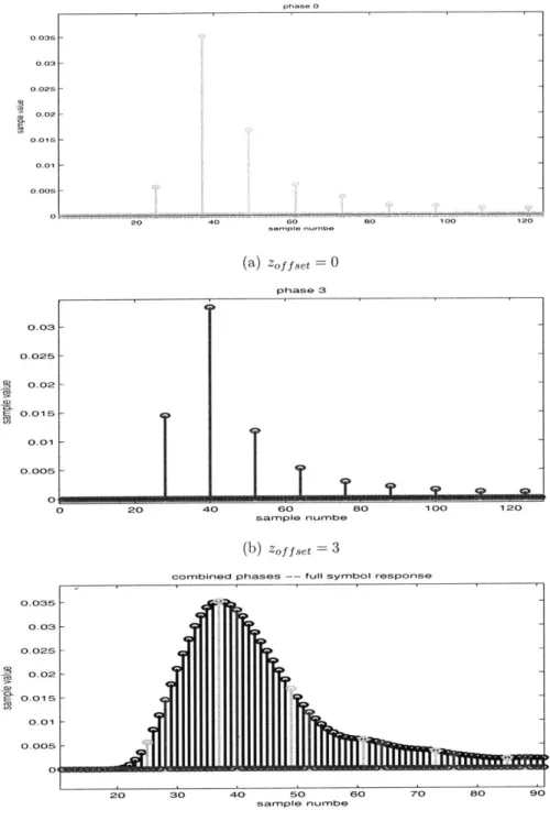
2-9 Phase sweeping process for extracting multiple sampling phases of the SR .. . . ... ... . . . .. ... .. .. . .... .... .. 52
3-1 Transmit equalizer block diagram . . . . 60
3-2 Differential switch - basic building block for tap-sharing txEQ imple-m entation . . . . 61
3-3 Transmit equalizer block diagram . . . . 64
4-1 Code hierarchy and linking: transmit pre-driver, transmit equalizer and receiver equalizer circuit formulations and signal description for-mulations before and after the receive equalizer can be seen. Red colored variables are exported to appropriate higher hierarchy level, while blue ones are selected internal variables. Linking level connects the appropriate interface variables. . . . . 77
4-2 Pulse response @ 4Gbps (i.e. the channel response to a 250ps-wide unit pulse) . . . . 79 4-3 Comparison of the solver generated and ideal equalized pulse response
for a given system level parameters . . . . 80 4-4 Model power change as a function of sampling phase . . . . 81 4-5 Pulse response A 6.25Gbps . . . . 84 4-6 Comparison of the solver generated and ideal equalized impulse
re-sponse for a given system level parameters @ 6.25Gbps . . . . 85 4-7 Model power change as a function of sampling phase . . . . 86 4-8 Pulse response L 8Gbps . . . . 88 4-9 Comparison of the solver generated and ideal equalized impulse
re-sponse and eye diagrams for a given system level parameters A 8Gbps 90 4-10 Pulse response A 10Gbps . . . . 91
List of Tables
2.1 Transmit equalizer (txEQ) system level variables . . . . 41
2.2 Receive equalizer (rxEQ) system level variables . . . . 43
2.3 Slicer system level variables . . . . 44
4.1 Design parameters for different sampling phases at 4Gbps . . . . 83
Chapter 1
Introduction
In this chapter we discuss the need for a new, more coherent approach to design of mixed-signal and analog integrated systems, focusing in particular on a high-speed link example. We discuss similar attempts or significant previous work and point out the technologies and conclusions we rely on. Further on, we introduce an example: a high speed link design. After describing performance measures for our example design, we focus on the difficulties of the traditional design flow. Finally, we introduce the formal description and setup of our example.
1.1
Motivation
Design of modern mixed signal integrated circuits is becoming increasingly difficult, mainly due to transistor scaling and always increasingly challenging performance specifications. Continued MOSFET scaling is approaching the global power dissipa-tion limits while increasing transistor variability, thus requiring careful allocadissipa-tion of power and area resources to achieve increasingly more aggressive performance speci-fications. Designers manage to overcome these challenges by modifying topology and better budgeting at the system level. However, the design cycle is becoming longer and more expensive [1]. One possible aid to this problem is creating a design flow that would provide tighter interaction between design hierarchy levels thus enabling faster design prototyping and design space exploration.
Currently, the mixed signal design is done in an iterative loop where system and circuit designers take turns, redesigning respective levels of design hierarchy. Usu-ally, one of the biggest challenges is connecting the system performance and resource allocation (e.g. power/area) estimate with subsystem performance, while providing realistic estimate of achievable designs at the circuit level. Usually, the system level designers start by assuming certain performance at the physical level. With these in mind, they design system level and define the necessary sub-system performance. After this system level budgeting is done circuit designers try to implement it. This design attempt will provide system designers with new information about achievable sub-system performance, and the iteration is repeated. Such iteration is performed until the assumptions taken at the system level happen to match the achieved per-formance at the circuit level; at this point the design loop converged.
With modern technologies it is not easy to predict performance before the actual design phase. The difficulty is due to smaller slack on specifications designers have, more complicated transistor modeling and harder trade-offs as the technology scales and device variability increases. Thus, even relatively small changes in specifications might prove to be challenging, requiring significant effort from the circuit designer, or even prove to be infeasible. Such sensitive design environment usually leads to a bad first estimate, and the design loop we described takes several iterations to converge. With increased design time costs this is becoming expensive and one of the main drawbacks to efficiently designing complex systems [1]. Furthermore, as average system complexity and size increase, power efficiency and area are becoming
as important as meeting the performance specifications.
Our aim in this thesis is to develop a design flow that brings system and circuit models jointly to a solution. We rely on system and circuit designers to provide reasonably accurate models of respective levels of design abstraction. Provided with such models, in a certain form, we plan to use optimization engine to explore the joint design space outlined by them. This approach, the system and circuit models are solved 'aware' of each other, and all inter-dependencies are guaranteed to be satisfied.
A good example to demonstrate this design methodology is a high-speed link (HSL). Basically, any data communication path in modern microprocessors, network communication equipment, etc. can be considered a HSL, [26, 18, 42]. Due to wire bandwidth limitations, HSLs are becoming more complicated systems, while on the other hand being tightly constrained by power, area and speed requirements due to high density of integration. These are very challenging and opposing system require-ments and interconnects still draw significant portion of power in modern designs [27]. Initial system design-redesign phase can take many turns before an acceptable design is achieved, and this process can include even some unsuccessful prototypes, thus increasing design time and cost significantly.
1.2
Previous work and important technologies
Developing a design flow assumes developing underlying CAD infrastructure as well as demonstrating actual circuit and system models. With this in mind, the previous work can be divided into two main areas: 1. optimization-aware modeling and optimization methods, and 2. circuit and system design and modeling.
To develop an optimization-driven framework we rely on many relatively recent results in optimization technology, optimization driven circuit design and appropriate tools. The optimization technology improved significantly in last couple of decades by introduction of interior point methods for convex mid-sized optimization problems. On this theoretical background most of the new solver infrastructure was imple-mented, resulting in high quality solvers for certain types of optimization problems such as the geometric programming, generalized geometric programming, linear pro-gramming, etc. The main challenge from this perspective is translating our system and circuit models into appropriate form that can be efficiently solved with a stan-dard optimization tool. For a good overview of the optimization in practical settings the reader is referred to [3].
This recent progress in the field of mathematical programming prompted a lot of work in attempts to apply these new achievements in engineering. The success
rate varies, and there are, still, many types of problems that appear in engineering applications where optimization theory still cannot give satisfactory solutions in an efficient manner.
As always, with no exact solution known, we see a lot of work in heuristic convex relaxation or brute force methods. Some work that is very relevant for the material laid out here can be found in [9, 23, 22, 12, 14, 13, 11]. In these reports the au-thors introduce assumption that transistor model can be represented in simple form through 'monomial' functions (i.e. generalizations of the power-function in multiple dimensions x" - x -), and that performance measures of circuit blocks can be ex-pressed in the generalized geometric (GP) programming form [3] starting from the transistor model parameters.
One should keep in mind that these works assume process technology nodes that were significantly easier to model than the current sub-100nm process nodes (the quadratic-law transistor model was reasonably good approximation of the measured results). Also, these works were circuit oriented without any treatment of the system level design and modeling. Furthermore, polarization of the circuits was usually omitted from the model and left to be checked once the solution is obtained. The significant contribution of these works is that they laid out the basis for the use of convex programming in circuit design [23, 28, 9, 22] and with further refinement (in terms of more accurate signomial-based models and appropriate solver extensions to handle signomial formulations like branch&bound guided convexification and GP approximation) represent the basis for our optimization-based approach. Out of these works, the GP-like optimization engine used in this work was derived.
1.2.1
High-speed link example
Serial links feature fairly complex system topologies. Usually multiple bit streams are serialized by a multiplexer, after which they are passed through pre-driver in-verter chain that serves as a link between digital logic (usually utilizing minimum size transistors) and analog transmit equalization filter that also serves as the out-put/channel driver. The clocking of the transmitter is derived from a phase-locked
loop (PLL). After the channel, the receiver signal path starts with an analog peaking amplifier/equalizer, followed by the clock-and-data recovery (CDR) loop. Finally, the de-serialization is performed, thus recovering the original bit streams.
As links do not perform any useful computation or processing but directly in-fluence the performance of the system as the interconnect infrastructure, it is quite natural to desire highest performance for a low price in terms of area and power consumption. One interesting problem with high speed links is strong coupling be-tween sub-systems. This is quite different from mainstream digital design where many blocks can be treated separately. This is not possible in the HSL design. As an ex-ample we can see the interaction of transmitter and receiver equalizers: they both perform almost the same task. The question that arises immediately is: which one is better? Do we need both? How should the link resources be allocated? Due to this complicated interactions of the building blocks performances designers still do not have final answers or methods to answer these types of questions in full and do it ef-ficiently. In such conditions designers try to simplify situation by introducing certain assumptions [21]. At times, the meaning and justification for such assumptions is not clearly expressed and it can be challenging to interpret the resulting trade-offs and impact of the assumptions we introduced. Furthermore, in the traditional design flow it is hard to formally write many such constraints and get insight into system/design sensitivity to them. Our goal in this work is to provide a more structured approach to express design constraints at the system and at the circuit level, and to do so in an unified manner.
Most generally, system level designers can apply any of the techniques developed in communication theory to high speed links. As always, there are certain aspects of the high-speed link design that are very specific and we should consider them when making initial assumptions and deciding on topology and system level functionality. As an example, we can notice that designers of HSLs seldom make use of coding techniques. While this is unusual, at first, as coding can increase the effective data rate helping to achieve the channel capacity, this choice makes sense once we take into account the complexity of decoder implementations, throughput requirements in
case of a HSL and the power overhead at such high data rates, [42].
In general, a good overall treatment of the high-speed link specific design and modeling issues can be found in [43]. It covers both system and circuit design, and describes the high-speed link environment and general setup. For this thesis the most important conclusions from [42] would be ones that have to do with system level design (equalization especially), the link environment, and link performance analysis to some extent. A possible extension of the work to be presented here might be incorporating timing jitter model into developed flow; for which a model is proposed in [431.
A simulation-based tool with a similar purpose to the one we are developing was described in [5], along with some modeling insights. There have been a couple of interesting simulation-based circuit optimization attempts, such as [31]. However, simulation based approach requires immense computing power in and does not scale beyond circuits with tens of transistors and simple simulation requirements [31].
1.2.2
Contributions of this thesis
To the best of our knowledge, major and original contributions of this work are
1. The first attempt to show an unified and highly structured flow for unified circuit and system design of HSLs
2. Robust system level formulation utilizing MOR-like techniques and transforma-tions to enable efficient parsing and solving
3. HSL design space exploration and tradeoffs
" Power consumption versus sampling phase choice
" Power allocation between predriver, transmit and receiver equalizer " Interaction between transmit side and receive side equalization efforts
1.3
High-speed link design
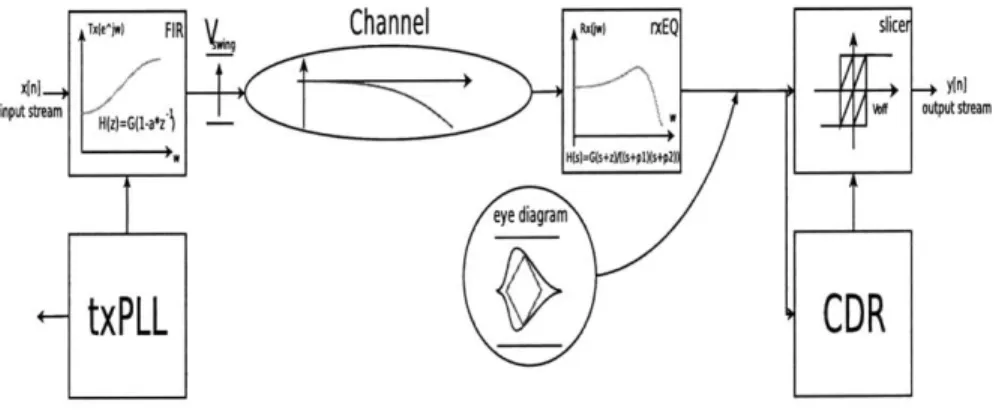
A system level model of a high-speed link is shown in Fig. 1-1. The transmit and linear receive filters are needed as equalizers in order to compensate for the frequency-selective (predominantly low-pass) channel characteristic. The effect of PLL and CDR jitter can be included through effective voltage noise models [43].
We aim to offer an answer to very important questions when new high-speed link design is being conceived:
" how limited resources (power, area/complexity) should be allocated in the de-sign
" what are the operating conditions of the circuits in the filter chain
" what is a reasonable (initial) design for these circuits
Our main goal is to answer these questions in relation to the ultimate performance measure for a high-speed link: the bit error rate (BER). In the light of our previous discussion our final goal is to try developing a flow that can help designing high-speed link with a certain performance (BER) for a given data rate, with as low as possible power consumption and bounded area. The design variables we are considering are: transistor sizes, biasing conditions such as polarization currents and voltage refer-ences, tap coefficients in digital equalizers and pole-zero placement of analog peaking
Tx*^jw FIR V
Channl
Rxv rE siinpu ShMotu H(z)sG(1-azzs) -)
~s)=tis
hreye diagram
+txPLL
r-
CDR
amplifiers. Thus, quasi formally we can express our design goals as the following optimization problem:
min Power
st. estimate(BER) < BERdesired
estimnate( Area) < Areadeired
circuit biasing constraints
variables : Ws, Ls, currents, equalization coefficients,
For simplicity, we focus on the signal processing chain in a link. We do not model any jitter or timing inaccuracies effects introduced in the circuits. To the first order this is justified as the residual ISI is the dominant error mechanism producing order of magnitude more errors than jitter-induced errors [42].
1.4
Summary
In this chapter we introduced the necessity of jointly solving circuit ans system levels for tightly constrained designs. We introduced the general idea we will use to approach the problem of system and circuit joint co-design, and introduced the most relevant past work that we base our method on. Finally we defined a concrete system we will use as a vehicle to demonstrate the performance of the method.
Building on the previous work in the field of equation-based circuit optimiza-tion we devised a set of MOR-like transformaoptimiza-tions that enable compact and robust formulation of the system level model of a HSL. Using this formulation enables us to formulate circuit and system (joint) optimization problem that is tractable and accurate.
Chapter 2
System level design
This chapter is dedicated to the system level model and design formulation. We will see how we can estimate the BER of the system, and what are the assumptions that need to be taken in order to do so. Furthermore, we will explain the subsys-tem integration and interface variables we pass between layers of the syssubsys-tem model abstraction.
From the formulation point of view we will see how certain problem-specific obser-vations can help us reduce the problem size. This will have big impact on our ability to formulate the optimization and use this flow.
2.1
System description
Here we explain the purpose of each sub-block of the system level and their mutual interaction at the top level of the design.
A high-speed link model we will be referring to in this chapter is shown in Fig. 1-1. We will, to the first order, distinguish between two main sub-systems:
" the signal processing chain and " the timing/clocking subsystem.
In the simplest model, these two subsystems operate in different domains: sig-nal processing is mostly observed through operations in voltage/current domain; the
clocking is an auxiliary subsystem needed for synchronization and could be modeled as an superimposed imperfect timing in the ideally synchronous core link. Alterna-tively, it can be modeled as some perturbation of the ideal signal processing result
[41].
2.1.1
The signal processing chain
The core of the link, in our case, is the signal processing chain consisting of " transmitter predriver
" transmit equalization FIR filter " the channel
" linear receive equalizer (peaking amplifier) " slicer/latch
Before we proceed we should define a couple of terms to be used.
Symbol response (SR) can be defined for linear systems. It is, basically, the con-volution of the impulse response of the channel and the symbol (basis function) used for communication. 1 If bit-space sampling is used it is the representation of the channel response at a certain sampling phase.
Sampling phase is the relative position within the symbol interval where receiver decides on transmitted symbol. In the HSL the clock and data recovery (CDR) subsystem determines the exact location of the sampling phase.
Main tap is the largest sample in the bit-space sampled SR, Fig. 2-1(a), of the system. This is the relative position where we expect forming of the appropriate sampling value. 2
'It has been observed that SR cannot be defined for certain single-ended systems as their falling and rising edges are not symmetric, thus, in binary communication, symbols 0 and 1 cannot be expressed using the same waveform. However, most of modern serial links operate in differential mode and this issue does not exist.
2
The position of the main tap is always found from the SR of the system. While this is influenced by the SR of the channel, this position can and will be changed due to effects of equalization, as we can see in Fig. 2-4(a) and Fig. 2-4(b). We will discuss this in much more depth in the section on equalization.
The channel
We refer to any type of medium used for transmission of data as the channel. In our example, it is some type of electrical interconnect (i.e. off-chip PCB traces, on-chip global routing layers, ...). We show a typical impulse response in Fig. 2-1(a) and the corresponding transfer function in Fig. 2-1(b). In case of oversampling the SR is convolution of the impulse response and symbol waveform, as we have mentioned.
Transfer function [dB] 10 -20 -30--40 -50 -60 -701-0 2 V 4 6 a 18 12 2 4 6 8
samp le numbef frequency [GHz)
(a) Typical SR of a channel (b) Typical transfer function magnitude
Figure 2-1: A 32 inch off-chip interconnect example
In this work we model the channel as an FIR filter. We chose this representation because it is easy to obtain from S-parameter measurements. It is also very convenient for automation as it is straightforward to switch between time and Z-domain in this form. Finally, any system can be represented in this form, to any desired accuracy.
From Fig. 2-1(b) we see that for a typical interconnect channel the -3dB band-width and the Nyquist frequency of signaling for gigabit rates are widely separated. On average, in high speed links, channel attenuation at the Nyquist frequency seems to be between 15dB and 30dB [41] which means that -3dB bandwidth can be at a frequency that is more than one decade lower than Nyquist frequency. Under these circumstances it is difficult or impossible to recognize incoming bit stream at the receiver side and we are forced to use equalization in order to reconstruct the
information [38, 15, 35, 41]. 6 main tap 0.14 pre-cursos 0p06scursoi4 0.04 0.02
Equalization: bandwidth extension model
Traditionally, in communications we treat equalization as an aid in achieving less in-tersymbol interference by extending the bandwidth of the system [43]. The intuition behind this approach is drawn from the frequency domain analysis of linear systems: extending bandwidth enables more of the significant components of the transmit-ted waveform to be passed through the system, thus providing higher fidelity when comparing input and output waveforms.
Note that this technique applies equally to analog and digital communication sys-tems. This is due to the fact that with this approach we set our goal to be preservation of the transmitted signal waveform despite the channel filtering. This approach can be formalized as Least Mean Square (LMS) parameter estimation problem [6, 39].
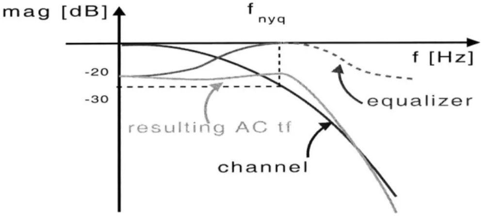
As HSL channels are predominantly low-pass, this bandwidth extension is achieved by introducing the high-pass filters at the transmitter or receiver side. The basic idea behind this equalization scheme is presented in Fig. 2-2. Ideally, we would invert the degradation introduced by the channel in full which is known as zero-forcing equalization (ZFE) [6], due to the fact that it removes all the ISI. The ZFE attempts to make the system response perfectly flat in the range of interest, as we explain in Fig. 2-2. This means that significant peaking might be necessary in order to counter-act the attenuation at high frequencies, Fig. 2-1(b). In Fig. 2-2 we see the channel characteristic in blue. The digital transmit-side equalizer transfer function is given in red up to the Nyquist frequency, and in dashed-red above for another Nyquist range. The resulting transfer function is given in green. The resulting transfer function (the green curve) should be an approximation of the flat all-pass filter in the range of the significant spectral components of the transmitted waveform. However, this is not always possible [6].
In the presence of noise, inverting the channel would amplifying the noise at high frequencies significantly, and potentially reduce the signal-to-noise ratio (SNR) [43]. Under these circumstances we employ the Unconstrained Minimum Mean Square Er-ror (U-MMSE) ' [39, 24, 41]. We note that one significant difference between ZFE
3
and U-MMSE is the objective function we are optimizing for. For ZFE algorithm the objective is minimization of the ISI. On the other hand, in U-MMSE the objec-tive is constructing equalizer that minimizes energy of errors (in a certain period of time) in presence of noise. In order to make this model more realistic, additional con-straint limiting the maximum output voltage from the transmitter (a concon-straint that is present in every circuit topology) can be introduced. Such optimization problems
are sometimes called Constrained MMSE (C-MMSE) [8].
mag
[dB] nyq -20 f [Hz] -20 -30equalizer
resUlting AG t f channelFigure 2-2: Principal idea of equalization
Finally, since in HSL environment the ISI is the dominant error generating mech-anism [42], our objective can be reduced to the maximization of the eye opening. In such circumstances model becomes a Linear Programming (LP) problem [37]. This brings us to a different interpretation of the role of an equalizer in the digital com-munication system.
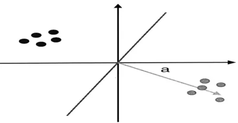
Equalization: symbol classification model
A different approach to equalization can be adopted from machine learning, machine vision and pattern classification. In this framework we construct equalizer to be linear separator of symbols in the received constellation [6, 16, 10]. The main idea of this approach can be seen in Fig. 2-3, for the case of binary signaling.
Here we can see two different sets of received symbols. In binary communication framework we can interpret each set as possible coordinates in equalizer state space
A kL
Figure 2-3: Separation of two non-intersecting sets
for different symbols being transmitted. Existence of multiple points in each set is clearly due to intersymbol interference as received values will depend on the particular sequence of symbols surrounding the symbol we try to decide on. Similar analysis is presented in [6].
In Fig. 2-3 vector a is, actually, vector of equalizer coefficients. We can observe that this vector has positive inner product with all the points in one of the sets, and negative inner product with points in the other set. This is equivalent to the existence of the separation hyperplane presented in the picture in red color. More on separation of sets can be found in [32, 29].
We can note that this approach does not, necessarily, try to match waveforms at the input and output of the system. Thus, this method is not suitable for analog communication systems. In these settings we are exploiting the fact that we are communicating in digital domain and the only function of equalization is to provide easy detection of the symbol which is easily associated with separation of sets. This is, exactly, the difference between the objective functions used to derive ZFE and MMSE versus eye maximizing LP program, as we have discussed in the previous section.
Transmit equalization FIR filter
This basically analog subcircuit has two main purposes:
* power amplification and impedance matching with the channel
* filtering to ameliorate severe intersymbol interference (ISI) generated in the channel
This analog front-end serves as a gateway from digital-logic's discrete time domain where we operate in terms of symbol-streams into analog domain where appropriate analog continuous-time representation of the bit sequence is transmitted over a lossy channel. It can be modeled as a very simple D/A converter.
The filtering operation is performed on a per-symbol basis. Thus, this module is a digital filter and has, to the first order, periodic magnitude of the frequency response. Since it is per-symbol filtering, the Nyquist frequencies of signaling and the Nyquist frequency of this filter cdincide. Usually, the transfer function of such a filter is written as
N
txF(z) az-k (2.1)
k=O
assuming that we only consider sampling times that are Tbit apart. Here we will introduce a slightly more general notation. We will assume that we have oversampled this system with oversampling ratio ovsRate. Under these circumstances, the transfer
function of this filter will be
N*ovsRate
txF(z) = amod(j, ovsRate) zd (2.2)
j=0
where mod(a, b) is standard notation for reminder of integer division. The reason for this 'complication' will become clear when we talk about CDR and sampling phase, as well as when we consider problems rising in debugging and the utility of an eye diagram.
As we can see in Fig. 2-2, high-pass transfer function in transmit equalization filter is achieved by attenuating the signal at low frequencies. The source of this attenuation can be traced to the circuit implementation of the filter. As it has to be a feasible circuit, we always have some maximum output signal swing that we can
achieve. For example, we can rarely achieve more than supply voltage, unless special techniques are used. More often some other constraints would limit achievable output swing. What this means at the system level is that for all the possible bit sequences the output from the transmit equalization FIR filter has to be limited. We can safely assume this limit to be unity, and scale appropriately. This means that
N
E akI 1 (2.3)
k=1
This equation is usually referred to as the peak power constraint or the peak swing constraint. Usually, some of the equalizer taps are negative, so DC gain given by
N
ak = txF(z - 0) (2.4)
k=1
is usually less then 1. In order to achieve some peaking and extend the bandwidth of the system through transmit side equalization we have to sacrifice the gain of the system. This is a very important property that brings up many questions about efficiency of transmit side equalization and trade-offs with receiver side equalization. Another important aspect of the equalizer is the delay it introduces in the signal chain. In Fig. 2-4(a) and Fig. 2-4(b) we can see two examples of equalized single bit response (SR) for two transmit equalizations with the delays of d = 0 and d = 1, respectively. It is obvious that by allowing for longer delays we potentially perform a better equalization as we can take into account not only the post-cursors in the SR, but some of the pre-cursors as well, Fig. 2-1(a). The tradeoff is observed in the fact that filters with a delay move relative position of the main sample in the SR vector. We should note that increasing delay in order to perform a better equalization is acceptable in systems which can tolerate delay but need as much bandwidth as possible. However, in systems which have very short delay and require small flight time (possibly some on-chip links), such approach might be undesirable.
As this work is a proof of concept we will mainly consider d = 0 transmit equal-ization settings, as it is easier to perform debugging and think about signals in this way. It should be straightforward to extend this to arbitrary delay by removing some
0 0.3 0 0.2 0. 0.1 0. 0.0 - 0.0 0. 0.3 0. 0.2 0. 0.1 0. 0.0
Comparing unequalized and equalized pulse response for d-O .4
unequalized syrnbol-sampled pulse response
5I -. 3rd order equalizer d-O
.3 -eye aperture is -0.122 5 -- eye aperture is 0. 169 2 1 - equalization coefficients: (0-66. -0.34. 0) 5 -0 2 4 6 10 12 14 16 18 2 sample number
(a) Second order FIR filter with delay d = 0
Comparing unequalized and equalized pulse response for d-1
4 1 1
unequalized symbol-sampled pulse response -0. 3rd order equalizer d-1 3- eye aperture is -0.12 eye aperture is .210 2-5 -1 1 equalizer coefficients: (-0.16.0.7.-027) 5[I 0 T 0 4
LT
3 -0.05 L 0 4 6 8 10 12 14 16 16 20 sample number(b) Second order FIR filter with delay d = 1
Figure 2-4: Delay of the transmit equalizer
of the constraints.
The optimal settings that maximize the worst case eye opening for transmit side equalization filter are known to be solution of a linear programming problem (LP), [37]. Furthermore, the peak swing constraint is straightforward to include. As the LP solver technology is well developed, it is easy to determine these optimal settings for a given channel and equalizer delay. We will talk more about worst case eye opening later in the text.
To combat reflections in the channel, the transmit equalizer output impedance is usually matched to the characteristic impedance of the channel (typically 500hm).
As this block also provides power amplification, the output transistors tend to be relatively large in size, and it is necessary to take into account their parasitic ca-pacitance. Otherwise it can severely degrade the performance of the system due to impedance mismatch, which causes channel degradation through reflections.
In case of an off-chip link, maybe even more serious source of parasitic capacitance are the ESD (Electrostatic Discharge) structure and pad capacitance at the output pad. This is introduced into the formulation as some fixed capacitance at the out-put. To take it into account we can follow the usual design procedure and impose a constraint that pole resulting from the output impedance of the equalizer has to be significantly higher in frequency than Nyquist frequency of communication. If it turns out to be a major drawback to the design, it would make sense to model it more accurately.
Linear receive equalizer
This is an analog front end in the receiver. It has almost the same functions as the transmit equalizer:
" match the impedance of the channel and buffer the signal before going into digital logic
" provide high-frequency peaking in attempt to extend the frequency range of the channel and decrease ISI
The main idea of this type of equalization is basically the same as for the transmit-side equalization, as we have explained in Fig. 2-2. The objective is to make overall transfer function as flat as possible in the region of interest. The region of interest is, again, defined as the range of spectral frequencies where transmitted signal has significant components. This is, of course, an attempt to make undistorted signal transmission. There are, however, some differences.
Firstly, this is a continuous-time system, which means that the transfer function is not periodic. Furthermore, the load of the output node is the input into decision
stage which might be less challenging to drive properly than the channel. Maybe most importantly, this block is capable of introducing gain into system transfer function.
Usually, this system is implemented as a selective amplifier with inductive peaking and transfer function
s
rxF(s) = G 2 (2.5)
or a system with capacitive source degeneration of a differential pair, producing sim-ilar peaking transfer characteristics:
1+
-rxF(s) = G (2.6)
(1 + ")(1 + ) )
In the first case the transfer function has complex-conjugate pair of poles produc-ing a peakproduc-ing characteristics. In the latter, the poles are always real, and we have to ensure such parameters that will produce the zero at the lower frequency than the poles, to achieve some peaking in the transfer function.
This is an analog system and to be incorporated into our formulation it has to be discretized. There are a couple of different approaches to discretization of an analog system (i.e. impulse invariance, pulse invariance, pole-zero mapping, ... ) [34]. For simplicity we usually employ the Tustin's mapping [34] as it enables simple and easy to track and debug interface between physical (circuit) parameters and top-level system parameters. The main concern when discretizing an analog signal is the accuracy of the digital approximation. This is directly related to the aliasing problem [33], and relatively high oversampling should be employed to accurately capture analog system behavior [34].
We will discuss the circuit model later on in the following chapters. At that point, we will also introduce the sampling method we used, in detail and give all the appropriate explanation. At the system level we only need the discretized Z-domain transfer function of the receive equalizer block. In our case, that means: equivalent gain and digital poles/zero locations.
Note that digital filters we derive from this circuit operate per-sample as opposed to per-symbol filtering of the transmit equalization filter. This is obvious from equa-tion (2.2) where we can see that transmit-side per-sample behavior is obtained by upsampling per-symbol response through zero-order hold.
To really answer a question of proper, implementation-aware equalization and system level design of a HSL we have to design a joint system and circuit optimization-based framework that can take all these effects into account.
Slicer/latch
This is a decision element. At this point in the receiver the transmitted bit sequence is being reconstructed from the received waveform. This block functions as a simple, but very fast, A/D converter. The performance of the whole link can be estimated from the knowledge of the signal quality and noise measure at the input to this block. It is often the case that slicer is being combined with FIR filtering in the feedback thus producing a nonlinear equalization structure known as decision feedback
equal-izer (DFE) [42]. This is especially the case with strong postcursor ISI where linear equalization is not powerful and efficient enough.
In our work we will not consider the DFE case. Modeling DFE at this (system) level is easy: we would just exclude certain number of postcursors from eye calculation, expecting the DFE to correct them. However, the circuit implementation might need some more attention as it is fairly complex subsystem. The goal of this thesis is to show potential of optimization-driven design flow in bringing circuit and system level design phases closer together.
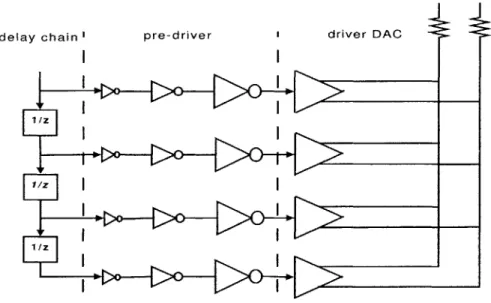
Transmitter predriver
Link designers use transmitter predriver as an interface between digital logic, usually being implemented in minimum size transistors, and transmit equalizer which presents significant input capacitive load due to large transistors we are forced to use in order to deliver significant signal power into the channel.
Implementation is usually very simple: inverter chain. Main contributions of this block are dynamic power and certain delay.
2.1.2
The timing subsystem
Both the transmitter and the receiver in a synchronous link need to have timing infor-mation. In our model, Fig. 1-1, the sub-blocks providing time-keeping functionality are transmit side PLL and CDR in the receiver.
It is customary to generate clocking for the transmitter by means of a phase locked loop (PLL) [7]. Such an architectural setup is convenient as only low-frequency clocks are distributed globally. This decreases number of high frequency lines in the design thus decreasing electromagnetic interference and power consumption. It is, also, necessary if the data rate is to be programmable or the reference clock does not meet timing jitter specifications.
The CDR loop is supposed to extract appropriate timing information from the incoming signal and adjust sampling phases in the receiver to optimally sample the incoming signal, if possible. It also contains some form of PLL.
The main trade-off in a PLL block is between clock quality in terms of phase noise/jitter and power [20] and it has been shown in [9] that circuit optimization can be used to assist this complicated trade-off. A reasonable design even for these blocks is somewhat dependent on the channel properties. All timing imperfections are being transmitted through the channel as edge modulation on the bit sequence [43]. Thus the overall effect, as seen at the receive end, is dependent on both PLL circuit and the channel.
While the effects of transmit jitter are, undoubtedly, important, they can be ameliorated with the appropriate equalization as it follows from the model in [43, 42]. This part of the system and its influence will not be considered in this work. For the time being, we will assume that we can perform ideal synchronization in the system. We will, however, try to provide an environment that is general and enables further manipulation of the data structures provided to make these kinds of extensions possible.
2.2
Performance metrics: BER and worst case eye
diagram
In our design objective for a HSL, we want to minimize power of the design, given performance specifications, as expressed in Formulation (1.1). Obviously, once the circuit constraints are met, system performance is expressed in terms of BER and power. Estimating power is straightforward from circuit model, once the circuit and system formulations are jointly described.
In order to estimate BER of a communication system designers usually consider signal and noise properties at the input of a decision element [431. Thus, the slicer decides based on the value of the sample at a sampling phase. Noise present in the system is usually modeled as AWGN coming from circuits and the channel. Consec-utively, system performance can be estimated once we can estimate sampled output value depending on the top level system parameters. This is achieved by constructing the eye diagram samples under worst case ISI at each sampling phase. Since ISI is dominant error mechanism [43] we use simplistic AWGN noise model at the input of the slicer with some given standard deviation.
In this subsection we explain how we construct the eye diagram. We look into influence of each sub-system to the eye diagram. Finally, we describe how we use it to find biasing conditions for circuits and how we try to calculate BER from it.
2.2.1
The eye diagram
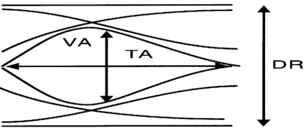
One of the most widely used tools to visualize performance of a digital communication system is the eye diagram of the signal at the input of the sampler (decision element). Open eye means that there exists a moment in each symbol frame where we can unambiguously decide which symbol was transmitted.
Ideally, it is obtained by overlying all the possible transitions during one symbol time on the same timing diagram. More practically, it is obtained on the scope or in simulation by overlying one symbol time long frames of the analyzed waveform,
which is usually transient response to a certain input symbol sequence.
D FR
Figure 2-5: Example eye diagram
An example eye diagram is presented in Fig. 2-5. Some of the most interesting characteristics are also indicated on the picture. The most interesting properties of an eye diagram are:
" voltage aperture (VA) - defined as the sampled value at the appropriate average sampling phase
" time aperture (TA) - defined as the horizontal (time domain) opening of the eye
" dynamic range (DR) - defined as the maximal deviation of the signal from the mean value
It is usually enough to know one sample phase of the eye in order to make a deci-sion. This means that we could, theoretically keep track of only symbol-space sampled SR of the system, and perform equalization according to the impact it makes to this particular sampling phase. Such approach would make sense from the formulation standpoint, as we have less equations to keep track of, thus saving in parsing and solving time and formulation file size. However, if we do keep track of one sampling phase only, we will not be able to provide any possibility to include the effect of the CDR to the system in the future. This is obvious if we remember that CDR operates by observing the symbol transitions (for example 0 to 1 and vice versa in binary
communication) while the data recovery path observes the signal at the appropriate moment between two transitions. Other way to note this is to say that the sampling clocks for data sampling and incoming timing extractions are, usually, in quadrature. Thus having multiple sampling phases of the eye diagram can be helpful dealing with the jitter and timing imperfections. Currently the optimization formulation we are providing needs to be given the sampling phase we expect the eye to be opened. With a little experimenting we can determine good candidates and proceed with other aspects of the design.
Finally, there is a strictly technical aspect of this choice to keep multiple phases. Having only one sampling phase makes debugging of the system level formulation much harder. In all equation-based optimization-driven design approaches one big issue arising is a debugging methodology. This is because we have only limited amount of data. As we noted before, the consequence of the presence of the designer in the loop introducing only relevant details. It greatly reduces the solution time thus improving the efficiency of this approach over simulation-based approaches. However, reducing amount of information can be a problem in debugging and testing phases, while a formulation is being developed.
Unlike with a simulation where we can observe many states of the system tracing the problem back to its cause, in optimization driven approach it is usually not pos-sible as we have only information on sensitivities of constraints that we specified. For example, if only one phase is available and the formulation cannot find an appropriate equalization to open the eye, we cannot know if the system does not have any chance of opening the eye, or the eye cannot be opened at that particular sampling phase. Having multiple phases inside the optimization run provides valuable information as we can see what the optimization engine is seeing in the system, and observe much more through analyzing decisions made for different sampling phases.
Thus, tracking multiple phases could be beneficial and we take that into account when formulating the system level optimization model. Through series of transfor-mations that we introduce, we manage to arrive to a simple, compact and reliable formulation, that enables quick parsing and solving and greatly reduces the
perfor-mance cost associated with keeping multiple sampling phases in the formulation.
2.2.2
Worst case eye diagram
If we agree to use the worst case scenario design, the eye diagram of the communi-cation can be simply calculated. As the usual SR of a communicommuni-cation channel has between 20 and 30, Fig. 2-1(a), significant samples this approach is well justified for low bit error rates (BER) of order less than le - 15, the usual HSL specifications. (We will verify this later and relate it to Fig. 2-7.)
In a (relatively rare) case of a channel that has many significant samples, this ap-proach can be too conservative as the worst case sequence estimated from a very long SR is very unlikely to happen. As an example we can note that 1015 is approximately expressed as 215. Thus this problem should not be considered unless the impulse response has more than (approximately) 45 significant samples. In the case of a very long impulse response some approximate analysis treating certain, reasonable, num-ber of most important samples in the SR as deterministic ISI and others as a source
of noise might bring more realistic results [431.
With previous discussion in mind, to determine the worst case input sequence, we start from the SR (ha) of the system. For the moment we will assume that the SR is bit-space sampled. At certain moment T we have, at the output of the system:
N
YT = hkbT-kAT (2.7)
k=1
which is just the convolution between SR of length N and the incoming bit sequence
bk. Suppose that the main tap of the system in question is at position hm. Suppose
also that we have transmitted symbol 1 (in binary case). The worst case scenario would yield sampling value of
N
ST = hm - I |hkI (2.8)
k=1, k$m
produces the main tap at time T and it is considered to be 1 (we assumed symbol 1 is being transmitted). All the other bits that produce any significant interference (basically those bits whose SR overlaps with sampling time T) are chosen in such a way to inflict maximum destructive interference at time T. This basically means that they are chosen according to the following formula
bT-(m+j)AT = -sgn(hm+j) (2.9)
where
j=-(m-1),...,N
-m andj
m.The same procedure we just described in case of symbol-space sampled SR can be performed in case we have an oversampled SR. The only modification is to carefully account for the interference at any point as it is still constructed from the symbol-spaced samples. For example: should we have a SR oversampled with ovsRate the worst case sample at any sampling phase k would be
N
s =hk - Jhj| (2.10)
j=1, jok, mod(j-k,ovsRate)=O
which is just a generalization of Eq. (2.8). As the waveform acquired in this process is longer than one symbol interval, it cannot be the eye diagram. An explanation is due.
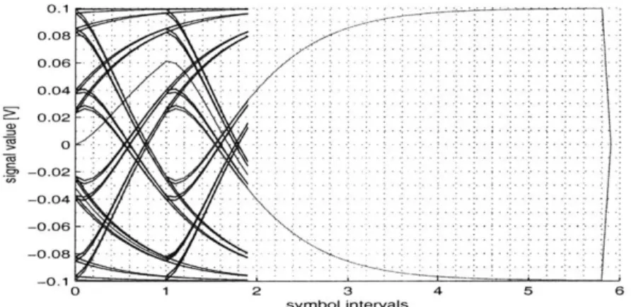
In Fig. 2-6 we can see how this waveform can be used to construct the real eye diagram. We also note that for clarity only one side of the real eye is shown. The other side we can be obtained by mirroring around the axis, or equivalently taking the negative of the lower part to get the upper part of the eye. We refer to this waveform as the unwrapped worst case eye.
In Fig. 2-7 we compare a simulated eye diagram (in blue) with the unwrapped eye (given in red). The unwrapped eye we calculate according to Eq. (2.10), while the eye diagram was obtained from a simulation for the channel presented in Fig. 2-1(b), by transmitting a pseudo random bit sequence (PRBS).
As we can see from Fig. 2-6 and Fig. 2-7 this waveform contains all the significant information provided by the eye diagram: voltage and time aperture and the dynamic