Publisher’s version / Version de l'éditeur:
Journal of Solid State Chemistry, 201, pp. 35-40, 2013-02-10
READ THESE TERMS AND CONDITIONS CAREFULLY BEFORE USING THIS WEBSITE.
https://nrc-publications.canada.ca/eng/copyright
Vous avez des questions? Nous pouvons vous aider. Pour communiquer directement avec un auteur, consultez la
première page de la revue dans laquelle son article a été publié afin de trouver ses coordonnées. Si vous n’arrivez pas à les repérer, communiquez avec nous à [email protected].
Questions? Contact the NRC Publications Archive team at
[email protected]. If you wish to email the authors directly, please see the first page of the publication for their contact information.
NRC Publications Archive
Archives des publications du CNRC
This publication could be one of several versions: author’s original, accepted manuscript or the publisher’s version. / La version de cette publication peut être l’une des suivantes : la version prépublication de l’auteur, la version acceptée du manuscrit ou la version de l’éditeur.
For the publisher’s version, please access the DOI link below./ Pour consulter la version de l’éditeur, utilisez le lien DOI ci-dessous.
https://doi.org/10.1016/j.jssc.2013.02.002
Access and use of this website and the material on it are subject to the Terms and Conditions set forth at
Characterization of carrier states in CuWO4 thin-films at elevated
temperatures using conductometric analysis
Gonzalez, Carlos M.; Dunford, Jeffrey L.; Du, Xiaomei; Post, Michael L.
https://publications-cnrc.canada.ca/fra/droits
L’accès à ce site Web et l’utilisation de son contenu sont assujettis aux conditions présentées dans le site LISEZ CES CONDITIONS ATTENTIVEMENT AVANT D’UTILISER CE SITE WEB.
NRC Publications Record / Notice d'Archives des publications de CNRC:
https://nrc-publications.canada.ca/eng/view/object/?id=90b48cb0-8dc6-4ee8-8791-1c1c7ac31811 https://publications-cnrc.canada.ca/fra/voir/objet/?id=90b48cb0-8dc6-4ee8-8791-1c1c7ac31811
Characterization of Carrier States in CuWO
4Thin-Films at Elevated
Temperatures Using Conductometric Analysis
C.M. Gonzalez,* J.L Dunford, X. Du, and M.L. Post
Energy Mining and Environment Portfolio, National Research Council of
Canada, 1200 Montreal Road, Ottawa, Ontario K1A 0R6
Abstract: CuWO4 thin-films were deposited by pulsed laser deposition onto an
insulating substrate. The temperature dependence of the electronic conductivity of CuWO4thin-films was determined over the 100 °C - 500 °C temperature range
in a synthetic air atmosphere. Additionally, variations of conductivity at 300 °C and 500 °C have been measured for oxygen partial pressures (0.1 atm < p(O2) <
0.9 atm) in nitrogen. The apparent activation energy ∆Ea for the electrical conduction has been estimated. The study of the temperature effect on the electron transport properties of CuWO4 thin-films reveals the operation of two
temperature-dependent oxygen states. The effect of varying oxygen concentration on the electronic properties is discussed in detail. The electrochemical nature of the operating oxygen states for the 100 °C - 500 °C temperature range is deduced using a physicochemical model that relates electronic conductivity with oxygen partial pressure and temperature.
Keywords:
semiconducting metal-oxide, surface characterization, electron transport, conductometric analysis, activation energy, oxygen states.
1. Introduction
The physicochemical characterization of semiconductor materials and, in particular, the material surface characterization, is a fundamental tool for the
optimization of the performance of the devices and technologies that have a working principle based on the electronic conduction of semiconducting materials, e.g. catalysts, photovoltaics, diodes, transistors, electronic circuits such as printed circuit boards, chemical sensors and transducers. Since these technologies exploit mechanisms that operate through, or near, the semiconducting surface, performance optimization requires comprehensive characterization of the interacting interface [1-2].
* Corresponding author. Tel.: +1 16136686811; fax: +1 16139912384. E-mail address: [email protected] (C.M. Gonzalez).
The electron transport properties of semiconducting metal oxides (thin and thick films) are commonly dependent on both intrinsic and extrinsic structural parameters, temperature and, in general, surface interaction with reactive gas-phase species. In particular, oxygen species (O-n) produced through chemisorption of molecular oxygen have been found to influence strongly the charge transport mechanism and surface reactivity toward redox species. Temporal changes in the electrochemical nature of semiconducting materials, and in particular metal-oxide surfaces, are originated in i) electron transfer events promoted by the surrounding gas-phase species (chemisorption and, in general, surface chemistry), ii) formation of surface states such as holes, oxygen vacancies and diffusive electrons (temperature effect), iii) diffusion of bulk defects to the surface and migration of surface states to the bulk (temperature effect and chemistry) and iv) segregation of lattice oxygen at high temperatures [1,3-5]. In particular, the formation of oxygen species arising from chemisorption of molecular oxygen promotes significant changes in surface electrochemical potential. This process yields
temperature-dependent oxygen species (e.g. O2ˉ, Oˉ, O2-) that exist as a result of both
the adsorption of molecular oxygen and electron transfer reactions. Oxygen species promote the operation of electrical fields in the metal-oxide surface, modify charge carrier concentration, cause bending of the conduction level and shifts in the energy of Fermi electrons near the metal-oxide surface [3-13].
Experimental techniques which are applied to surface characterization of semiconducting metal-oxides comprise the phenomenological approach (e.g.
impedance spectroscopy and conductometry) [10-15], spectroscopic techniques such as X-ray photoelectron spectroscopy (XPS), IR and Raman spectroscopies, electron paramagnetic resonance (EPR) [16-21], and imaging such as transmission electron (TEM) and scanning electron microscopies (SEM) [22-25]. In the present work,
conductometric analysis is used to characterise the oxygen states operating in CuWO4
thin-films in the 100 °C < T < 500 °C temperature range and under varying O2 partial
2. Experimental 2.1. Materials
CuWO4was prepared using a solid state reaction of a molar ratio of reactants
CuO : WO3= 1 : 1. The reagents were used as received, WO3(Alfa Aesar, 99.998 %)
and CuO (Alfa Aesar, 99.995 %). Sintering of the reaction mixture was carried out at 600 °C for 12 hours under flowing O2. Compacted pellets of CuWO4for use in film
deposition were prepared by isostatic pressing (2 Tonnes) in a mold, followed by sintering at T = 680 °C for 24 hours in flowing O2.
Thin-films of CuWO4were prepared from the pellets using the pulsed laser
deposition technique (PLD).Thin-films were grown on single crystal sapphire substrates, α-Al2O3 , using a Lambda Physik LPX305i laser. The operational conditions of the
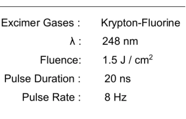
PLD process are described in detail elsewhere [26], and are summarized in Table 1. Films of approximate thickness ~ 200 nm were deposited and the thickness determined using profilometry (XP-2TM Stylus Profilometer, Ambios Technology, Inc.).
Table 1. Laser deposition parameters for the preparation of CuWO4nanometric
films.
Laser Deposition Parameters Excimer Gases : Krypton-Fluorine λ : 248 nm
Fluence: 1.5 J / cm2
Pulse Duration : 20 ns Pulse Rate : 8 Hz
2.2. Physicochemical Characterization
The laser target (CuWO4) and thin-films were characterized by X-ray diffraction
(XRD) using a Bruker-D8 diffractometer with unmonochromated cobalt radiation (λKα1=
1.78897 Å) and parallel beam geometry. The sample holder was stationary with both the XR-source tube and detector mobile. Phase determination was done by reference to
standard XRD patterns provided in the ICDD Powder Diffraction File Database (supplied as PDF-2 and compiled into DIFFRACTplusReference Database released in 2002).
Specimens were then examined using a JEOL 840A scanning electron microscope. All micrographs were obtaining using an accelerating voltage of 20 kV and a working distance of 15 mm.
The system for evaluating the electronic conductance of the films consisted of a custom-built computer-controlled system with a resistive heater (power supply Xantrex HPD 60-5), gas-supply manifold (MKS Type 1479A Mass-Flo®controllers) and Au
contact electrodes connected to a Keithley-2400 SourceMeter. For conductometric studies, gold electrode pads were deposited onto the thin-films using a thermal vacuum deposition procedure (Denton DV502A system) to ensure ohmic contact to the
measurement system electrodes. The electronic conductance (σ) was monitored to detect changes in the electron transport properties of the thin-films with changes in experimental conditions (e.g. temperature and p(O2) ). The gas sources for the
measurements were high purity O2(Linde, 4.5 grade) and N2(Linde, 5.0 grade).
Conductance was measured in two sets of experiments, initially with constant O2
concentration (pO2 = 0.2 atm, balance N2) with varying temperature (100 °C < T < 500
°C), and then under two isothermal conditions (T = 300 °C and 500 °C) with varying O2
partial pressure (0.1 < p[O2] < 0.9 atm). For all of the experiments, the total gas flow
rate was 250 cm3/ minute, and the total pressure, 1atm.
Prior to initiating conductometric measurements, the thin-films were annealed (T = 520 °C) in the test chamber for 48 hours under dry synthetic air (20 % O2 in N2) to
eliminate the interference of foreign surface adsorbates such as surface species arising from interaction with water vapor, CO2, CO, etc. The annealing treatment also offered a
means to annihilate unstable lattice defects that frequently form during thin-film growth, and allows the equilibration of the semiconducting thin-film with the background gas, thus promoting signal reproducibility. The thin-films were kept in the measurement chamber under dry synthetic air or the other O2/N2 mixtures for the duration of the
3. Results and Discussion 3.1. Structural Characterization
Figure 1 shows the XRDs for (1a) a representative CuWO4thin-film, (1b) the
PLD CuWO4target and (1c) the substrate α-Al2O3 .The formation of single phase
CuWO4was confirmed by comparing the XRDs for both the reaction product and the
PLD pellet with those from the database standard DIFFRACTplus– 2002 (CuWO
4
standard ID # 01-088-0269). No reflections from reagents were observed. The XRD for the PLD target (CuWO4), Figure 1b, displays the characteristic wolframite (triclinic)
pattern. As expected, the thin-film XRD (Fig. 1a) shows the substrate reflections. Since both the substrate (α-Al2O3) and the thin-film material (CuWO4) display XRD patterns
with reflections about similar 2θ angles, an overlap for some of the diffraction peaks occurred, specifically at 2θ ≈ 26.9° and 62.1°. This assessment is supported by a change in the observed order of intensity for the reflections arising from the substrate (compare Figure 1a with 1c). The thin-film XRD (Fig. 1a) displayed a reduced number of reflections compared with the bulk material. This suggests the formation of a CuWO4
film with a preferential orientation.
Figure 1. XRD spectra for (1a) a representative CuWO4 thin-film, (1b) the CuWO4
PLD target and, (1c) substrate α-Al2O3 .
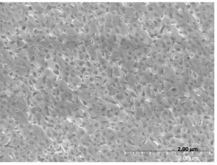
Scanning electron micrographs were obtained for a CuWO4thin-film, Figure 2. The micrograph shows distorted and elongated particles (5 nm to 100 nm) in contact
with larger grains. The majority of the smaller particles (grains) are embedded in the larger grains (> 500 nm).
Figure 2. SEM Micrograph of a CuWO4thin-film.
3.2.1. Temperature Effect on the Electron Transport Properties of CuWO4
Thin-Films
The electrical conductivity of semiconducting materials is a thermally activated process. Although transport of charge carriers across the semiconductor surface is a complex process, the electron transport dynamics is satisfactorily described by
Equation 1 [5-10,12-15,22,27-33]. This equation relates electronic conductivity (G) with temperature by means of an Arrhenius-like relationship (ln G
T 1
) Equation 1, G* is
an entropic parameter accounting for i) the granular morphology (grain size-distribution, quality of inter-grain contacts, crystal structure, lattice defects and surface states), ii) field effects arising from the coulombic charge of both the charge carriers and surface states (including oxygen states On-
)
, and iii) electron-lattice interactions[3-7,12,14,29,33]. G* is also a parameter that includes the influence on the surface by the gas-phase surroundings and accounts for the concentration of reactive gas-phase species (e.g. O2, CO, CO2, NOx, H2O, etc.). ∆Earepresents the energy required for the promotion of an electron in the proximity of the Fermi level (under the electrostatic
influence of surface states, including oxygen species) to a diffusive state, and kBis the Boltzmann’s constant. T kE exp * G G B a (1)
Differentiation of Equation 1 in logarithmic form (ln G) with respect to reciprocal temperature (
T1 ) yields Equation 2, which facilitates estimation of the activation energy ∆Eafor electronic conduction.
B a kE T 1 ln (2)
Equation 2 lists conductance σ instead of conductivity G. Within Drude’s model of electronic conduction, the conductivity GD and the conductance σ are related by
Equation 3, where A represents the cross-section of the conducting material and ℓ, the corresponding length.
A
GD
(
3)
Parameters A and ℓ (Equation 3) can be considered to be nearly independent of temperature (that is, for materials with small coefficient of thermal expansion, which is often the case for ceramics). Substitution of G by the related parameter σ (Equation 3) in the derivative of Equation 1 with
T 1 (that is, T 1G ln ) leads to Equation 2. Figure 3(ln R vs. T
1 , where R is the measured resistance) shows the
temperature effect (100 °C < T < 500 °C range) on the electron transport dynamics of a CuWO4 thin-film in dry synthetic air (20 % O2in N2). The electronic conductance (σ)
increased with temperature (ln R increased with T
1 ), which agrees with the thermally activated nature of the electron conductivity in semiconducting materials. The Arrhenius
plot in Figure 3shows two distinct temperature domains. These domains are
characterized by a change in slope of the plot with an onset temperature, in this case T ~ 250 °C. For the thin-films under investigation, the temperature-dependent domains appear within 100 °C < T < 250 °C with ΔEa= 0.34 eV, and within 250 °C < T < 500 °C
with ΔEa= 0.17 eV. The lower activation energy ΔEafound for the latter temperature
range has been explained as a result of the increase in the number of charge carriers caused by an increasing number of unstable lattice oxygen atoms
[1,7,9-10,12,19,21,27]. Similar transition temperatures for electronic conduction have been previously reported for CuWO4thin-films; i.e. transition temperature T ~ 200 °C, ΔEa =0.57 eV for the 37 °C < T < 200 °C temperature range, and ΔEa= 0.12 eV for the 200 °C < T < 340 °C temperature range [23]. The temperature dependence of activation energy for electronic conduction ΔEahas been explained as a consequence of varying field effects in the semiconductor surface [29,33-45]. The electrochemical changes that the interacting interface undergoes with temperature result in the operation of
temperature-dependent field effects. The variation in surface electrochemical potential is related to i) a change in the electrochemical nature of oxygen species with
temperature (O2⟶ O2ˉ ⟶ Oˉ ⟶ O2-), and an associated variation in surface charge
and number of conduction electrons, ii) the coulombic interaction between conduction electrons and oxygen states (formation of a depletion layer and band bending), iii) the reversibility of oxygen chemisorption (destabilization of chemical bonding with
increasing temperature, e.g. desorption of oxygen states resulting in a rise in the number of surface electrons and a corresponding change in surface charge), iv) an increase in the segregation of lattice oxygen atoms and migration of oxygen vacancies from the bulk to the surface with increasing temperature, and v) the effect of
temperature changes on the electron-lattice interactions (e.g. increase in the electron scatter with temperature) [46]. For instance, for WO3thin-films, it has been reported that
O2ˉ adsorbates are stable below 150 °C and coexist with HOˉ surface species
;
at highertemperatures, O2ˉadsorbates undergo stepwise reduction to Oˉ (stable in the 150 °C < T
< 300 °C range). As temperature continues to increase, Oˉ will further reduce to O2-,
which is stable above T ~ 300 °C [40]. Whereas for SnO2 thin-films, water and O2ˉ
and 500 °C, and O2- above 500 °C [35,39,47-48]. Based on these findings, the
temperature ranges in Figure 2 can be explained as being a result of the formation of two different oxygen states as temperature increases.
Figure 3. Temperature effect (ln R vs.
T1
) on the electronic resistance R of a
CuWO4 thin-film for the 100 °C < T < 500 °C temperature range under synthetic air(20 % O2in N2).
The temperature dependence found for ΔEa(Figure 3) could also be related to chemical and structural changes in the thin-film with increasing temperature such as bulk changes in the crystal lattice or formation of oxygen-depleted phases. However, the formation of oxygen-depleted phases (CuWO4-δ) as temperature increases is not
likely to arise in the temperature range studied since the process would produce a significant change in the electron conduction profile with temperature (which would likely result in a discontinuity in the relationship of conductance with temperature, and in the evolution of a metallic-regime for conductivity as a result of the formation of an
extensive intrinsic doping) [49]. Moreover, the resulting oxygen loss will produce the parallel reduction of W6+(or Cu2+) because charge balance requires that for each
This process involves a substantial reorganization of the electron density and significant changes in bonding parameters and crystal lattice. Consequently, the changes in both coulombic and structural parameters will impede the return to the conductance value corresponding to a predetermined reference state (defined in this study for the
stoichiometric single phase CuWO4in synthetic air 20 % O2in N2). This situation did not
arise for the experiment summarized in Figure 3. Another factor to consider is a phase transition near the frontier temperature (for the case studied T ~ 250 °C). However, CuWO4does not undergo a lattice transformation in the temperature range studied [50].
3.2.2. Characterization of Operating Oxygen Sates by Conductometric Analysis Equations 4 and 5 summarize the formation of the oxygen species in
semiconducting metal oxide surfaces [4-6,31,48]. In the model below, O0x represents an
unstable lattice oxygen, VOn+a single or double ionized oxygen vacancy, and On’-
,
thecorresponding oxygen species (O2ˉ, Oˉ, O2-).
O0x ⇄ ½ O2 + VOn+ + n eˉ (4)
½ O2 + n’e- ⇄ On ’- (5)
Equation 5 defines the effect of oxygen chemisorption on the electronic conduction of n-type metal-oxide materials, which is manifested through a reduction in electronic conductance with increasing [O2]. The electronic conductivity G relates to the number of
effective charge carriers through Equation 6, where [eˉ] is the concentration of charge carriers that participate in electronic conduction assuming that the contribution of
positive charge carriers to the electric conductance is negligible, μ denotes the electron mobility and e, electronic charge [38-39,42-43]. Equation 6 shows the relationship of electronic conductivity G with the charge carrier concentration [eˉ] and reveals that a reduction in the number of surface electrons as a result of oxygen chemisorption (Equation 5) leads to a decrease in surface conductivity. For the temperature range investigated (300 °C < T < 500 °C), the expected oxygen species On’-are Oˉ or O
2-[22,33,35,39-40,47,49-51]. The charge conduction mechanism has been considered to occur through electron conduction since typically mixed ionic-electronic conduction occurs at higher temperatures (T > 700 °C) which promotes the formation of a
significant number of oxygen vacancies (VO2+) and the formation of oxygen depleted
phases with mixed valence states [51-52].
e eGD (6)
Equation 7 has been used previously to evaluate the effect of oxygen
concentration on the electronic conductivity of semiconducting metal-oxides [37,45,52-57]. In the model, pO2 is the oxygen partial pressure, n relates to the number of charge
carriers that participate in the electronic conduction as indicated in Equation 4, ΔEais, as before, the apparent activation energy for conduction. G’ is considered a constant, temperature-independent term, with the same physical meaning as G* outlined in Section 3.2.1 (Equation 1), except that in this case G’ is a parameter independent of the concentration of reactive gas-phase species. It has been established that the electron conductivity of n-type semiconducting metal-oxides under the influence of oxygen states in intermediate and high temperature ranges (Oˉ or O2-) is primarily
controlled by the rate for promotion of electrons to a diffusion state (Equation 4) and, to a lesser extent, on the formation of new oxygen states with increasing [O2], Equation 5
[39]. Formation of an increasing number of oxygen states with both [O2] and
temperature features a kinetics limitation, which is related to a limited surface for formation of oxygen adsorbates (saturation effect), and electronic repulsion effects (interaction between conduction electrons and negative oxygen species), and a thermodynamic limitation related to both the destabilization of oxygen adsorbates with increasing temperature (which is evidenced by the reduction of effective coverage with temperature), and an increase in oxygen vacancies at high temperature [12,57-61].
T kE exp ' G pO G B a 2 n 2 1 2 (7)
The slope of a plot for ln G (or ln σ) vs. ln pO2, Equation 8, allows inferring the nature of
surface oxygen vacancies VOn+available for bonding interactions with molecular oxygen
and consequently the electrochemical nature of the oxygen species in operation at the investigated temperature range. For the relationship
2 pO ln G ln , ln G can be substituted
by ln σ since the thin-film cross-section, A, and length, ℓ , both relating G with σ (defined in Equation 3), are not parameters of the O2concentration.
2 n 2 1 pO lnln 2
(
8)Since the oxygen vacancies (VOn+) are ideal structural sites for the
accommodation of oxygen species (On’-), it is reasonable to consider that oxygen bonding interactions take place through an intermediate of such surface defects. Therefore, the electrochemical nature of the oxygen-states can be reasonably inferred from the charge of operating oxygen vacancies at a given temperature (Equation 4) [62]. Based on these considerations, the electrochemical nature of majority oxygen-species can be related to the electrochemical nature of surface vacancies. The
equilibrium constant Ke, Equation 9, for the process represented in Equation 4 offers a simple means to evaluate the effect of surrounding O2on the electrochemical nature of
oxygen states [39,42-43,51,63]. Lattice oxygen concentration [OOx] is not considered for
the estimation of Kesince the corresponding concentration in equilibrium with gas-phase species is approximately constant at any given [O2] (ratio for number of OOxto
lattice volume ≈ constant).
1/2 2 n n O e V e pO K (9)Based on Equation 4, the mass-action law for formation of charge carriers requires that the ratio [VOn+] to [eˉ]condequals
n 1 e V cond n O
, which allows rewriting
concentration of effective charge-carriers [eˉ] and oxygen concentration (pO2ˉm) for
n-type semiconductors.
e cond KepO22n12 (10)
Based on Equations 4 and 5, the formation of oxygen species (On’-) requires an interaction of majority oxygen vacancies (VOn+) with surrounding molecular O2and the
removal of an equivalent number of electrons (n). Thus, the formation of Oˉ will require the interaction of O2 with a single ionized vacancy (VO+) and consumption of a chemical
equivalent of electrons e‒(n = 1). Therefore, for a system where the majority oxygen
state is Oˉ, the slope (Sl) for the corresponding plot for ln σ vs. ln pO2should be equal to
4 1
(as indicated in Equation 8, with n = 1). Similarly, if O2- were the resulting
oxygen-state upon interaction between surrounding O2and predominant double ionized oxygen
vacancies (VO2+), then n = 2, and therefore the slope of a plot ln σ vs. ln pO2 should be
6 1
. Based on this, the study of the effect of [O2] on the surface conductance will allow
evaluating the electrochemical nature of the operating oxygen states at constant temperature.
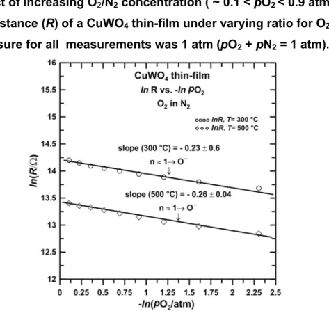
Figure 4shows the dependence of resistance (ln R) with the concentration of surrounding molecular oxygen (ln pO2) in N2at 300oC and 500 °C (total pressure 1atm).
The resistance R data for both temperatures can be defined as having a linear
relationship to ln pO2both with similar slopes (Sl), i.e. Sl(300 °C) = – 0.23 ± 0.06, and Sl (500 °C) = – 0.26 ± 0.04. These values as applied to the Equation 8 yield n ≈ 1 (as shown above, a slope of Sl~ 0.25 implies that the oxygen state On’-in dynamic
interaction with the surrounding molecular O2is Oˉ). The increasing resistance values
(ln R) with O2(ln pO2) is an indication of the n-type conductivity for the CuWO4
thin-films.
When differentiating Equation 7, the effective charge carrier mobility μ(defined in Equation 6) was considered to be independent of temperature, which is not strictly
true since μ∝ exp T k E B
, where Eμis the activation energy for electron mobility.
Nonetheless, for the present case this is a valid assumption, since the activation energy for mobility Eμof n-type semiconducting metal oxides is smaller than the activation energy for conduction ΔEa, usually by an order of magnitude [43,49,62]. For instance, in the case of bulk samples of oxygen-depleted tungsten oxides (WO3-δ), the estimates of
corresponding activation energies for Eμusing Hall mobility have been reported in the 0.01 eV < Eμ< 0.06 eV range, whereas for the same samples, the activation energy for electronic conduction was in the range ~ 0.1 eV < ΔEa< 0.2 eV [49].
Figure 4. Effect of increasing O2/N2 concentration ( ~ 0.1 < pO2< 0.9 atm) on the
electronic resistance (R) of a CuWO4thin-film under varying ratio for O2-to-N2.
The total pressure for all measurements was 1 atm (pO2+ pN2= 1 atm).
Since the operation of mixed conduction mechanisms usually produces sigmoid isotherms for plots of ln σ vs. ln pO2[40,52,62,65-67], the linearity of the relationship
between ln R and ln pO2for the isotherms in Figure 3 provides further evidence of the
operation of a charge conduction mechanism through diffusive electrons. The evaluation of the nature of oxygen states (On’-) for the thin-films under investigation using conductometry illustrates the potential of the method for studying semiconducting
interfaces and, by extension, for the study of surface reactions in catalytic processes that proceed through the intermediation of oxygen states On’-. The reasonable fit also
suggests that the CuWO4 films under study are free of impurities and that the
semiconducting metal-oxide surface reaches equilibrium with the surrounding gas
during measurement. In agreement with the temperature domains established using the Arrhenius plot Figure 3(which predicts the operation of two consecutive temperature-dependent oxygen states On'-, that is, a majority oxygen state that operates in the 100 °C < T < 250 °C range, and another majority oxygen state in the 250 °C < T < 500 °C range), Oˉ was the operating oxygen state identified at both T ~ 300 °C and T ~ 500 °C. Based on the results summarized above and other literature reports, the oxygen state operating in the 100 °C < T < 250 °C range can be assigned to O2-[22,33,35,40].
4. Conclusions
The qualitative description of surface species in semiconducting CuWO4
thin-films was carried using a model frequently invoked for the oxygen chemisorption process in n-type semiconducting metal-oxide surfaces. As established in a number of studies, the electronic conductance was satisfactorily characterized as a parameter of the oxygen concentration (G pO2m, where
2 n 2 1 m
) [
39-64]. In agreement with these reports, for the study under discussion the oxygen state On-operating in the intermediate-high temperature range (300 °C < T < 500 °C) was Oˉ. The agreement between theory and experiment indicates that, in the absence of moisture and other gas-phase species, the mode of charge conduction is through diffusive electrons, allowing eliminating a significant contribution from other charge conduction mechanisms (e.g. ionic conductivity, protonic conduction).This approach is an example of the use of a macroscopic property for
characterising chemisorbed species at the molecular level. Utilization of the physical model outlined herein for the characterization of extrinsic surface states, and, in particular, oxygen species requires the use of a single-phase semiconducting metal oxide. This work provides support for using conductometric analysis to study surface
states as a complementary technique to the spectroscopic characterization of semiconducting metal-oxide interfaces.
Acknowledgements
The authors thank the NRCan PERD-AFTER program for funding support for this work in activity C23.007. This article is recorded as National Research Council of
Canada, NRCC# 53116.
Bibliography:
[1] S. M. Sze, M.-K. Lee, Semiconductor Devices: Physics and Technology. John Wiley & Sons, 2012.
[2] H.L. Tuller, S.J. Litzelman, G.C. Whitfield, Chapter 10 Electrical Conduction in Nanostructured Ceramics. (Eds. R. Riedel, I.-W. Chen, Ceramics Science and Technology, Materials and Properties 2) Wiley-VCH, 2010.
[3] D. K.Aswal, Sh. Gupta, K. (Eds.) Science and Technology of Chemiresistors Gas Sensors. Nova Science Publishers, Inc. 2007.
[4] G. Pacchioni, ChemPhysChem. 4 (2003) 1041-1047.
[5] V.E. Bochenkov, G.B. Sergeev, Adv. Colloid Interface Sci. 116 (2005) 245-254. [6] H. Statz, G. A. Demars, Phys. Rev. 111 (1958) 169-182.
[7] N. Barsan, D. Koziej, U. Weimar, Sens. Actuators, B. 121 (2007) 18-35. [8] Q. Fu,T. Wagnera, Surf. Sci. Reports 62 (2007), 431-498.
[9] C. Malagu , V. Guidi, M. Stefancich, M.C. Carotta, G. J. Mertinelli, Appl. Phys. 91 (2002) 808-814.
[10] A. Varpula, S. Novikov, A. Haarahiltunen, P. Kuivalainen, Sens. and Actuators, B 159 (2011) 12-26.
[11] H. Geistlinger, Sens. Actuators, B 7 (1992) 619-625. [12] T. A. Goodwin, P. Mark, Prog. Surf. Sci. 1 (1971) 1-64.
[13] T. Sahm, A. Gurlo, N. Bârsan, U. Weimar, Sens. Actuators B 118 (2006) 78-83. [14] H. Geistlinger, Surf. Sci. 277 (1992) 429–441.
[15] S. A. Bilmes, D. Posadas, Colloids Surf. A 134 (1998) 47-57.
[16] J.-Ch. Dupin, D. Gonbeau, P. Vinatier, A Levasseur, Phys. Chem. Chem. Phys. 2 (2000) 1319-1324.
[17] D. Cappus, M. Menges, C. Xu, D. Ehrlich, B. Dillmann, C. A. Ventrice, J. Libuda, M. Bäumer, S. Wohlrab, F. Winkelmann, H. Kuhlenbeck, H.-J. Freund, J.
Electron. Spectrosc. Relat. Phenom. 68 (1994) 347-355.
[18] D. Cappus, M. Haßel, E. Neuhaus, M. Heber, F. Rohr, H.-J. Freund, Surf. Sci. 337 (1995) 268-277.
[19] A. P. Shpak, A. M. Korduban, M. M. Medvedskij, V. O. Kandyba, J. Electron. Spectrosc. Relat. Phenom. 156-158 (2007) 172-175.
[20] A.F. Carley, P.R. Davies, M.W. Roberts, Catal. Today 169 (2011) 118-124. [21] T. Herranz, X. Deng, A. Cabot, M. Salmeron, J. Catal. 283 (2011) 119-123. [22] M. Batzill, U. Diebold, Prog. Surf. Sci. 79 (2005) 47-154.
[23] P. K. Pandey, N.S. Bhave, R.B. Kharat, Mater. Lett. 59 (2005) 3149-3155. [24] J.-H. Lee, Sens. Actuators B 140 (2009) 319-336.
[26] Copper Tungstate Thin-films for Nitric Oxide Sensing. C.M.Gonzalez, X Du, J.L. Dunford, M.L. Post, Sens. Actuators B: Chem. (2012),
http://dx.doi.org/10.1016/j.snb.2012.06.067. [27] T. Ando, Rev. Mod. Phys. 54 (1982) 437-672. [28] P. A. Lee, Rev. Mod. Phys. 57 (1985) 287-337.
[29] K. Aguir, C. Lemire, D.B.B. Lollman, Sens. Actuators B 84 (2002) 1-5.
[30] D. Baresel, W. Gellert, W. Sarholz, P. Scharner , Sens. Actuators 6 (1984) 35-50. [31] M. J. Sienko, P. F. Weller, Inorg. Chem. 1 (1962) 324-331.
[32] Sahle, W.; Nygren, M. J. Solid State Chem. 48 (1983) 154-160.
[33] J.Ding, T.J. McAvoy, R.E. Cavicchi, S. Semancik, Sens. Actuators B 77 (2001) 597-613.
[34] J. Guérin, K. Aguir, M. Bendahan, Sens. Actuators B 119 (2006) 327-334. [35] D. Kohl, Sens. Actuators B 18 (1989) 71-113.
[36] G. Korotcenkov, B.K Cho, Sens. and Actuators B 142 (2009) 321-330. [37] G. Korotcenkov, Mater. Sci. Eng. B 139 (2007) 1-23.
[38] S. Saukko, U. Lassi, V. Lantto, M. Kroneld, S. Novikov, P. Kuivalainen, T. Rantala, J. Mizsei, Thin Solid Films 490 (2005) 48-53.
[39] J. McAleer, P. Moseley, J. Norris, D. Williams, J. Chem. Soc., Faraday Trans. I, 83 (1987) 1323-1346.
[40] W. Yu-De, C. Zhan-Xian, L. Yan-Feng, Z. Zhen-Lai, W. Xing-Hui, Solid-State Electron. 45 (2001), 639-644.
[41] K. Wetchakun, T. Samerjai, N. Tamaekong, C. Liewhiran, C. Siriwong, V. Kruefu, A. Wisitsoraat, A. Tuantranont, S. Phanichphant, Sens. Actuators B. 2011 In Press.
[42] P. T. Moseley, Meas. Sci. Technol. 8 (1997) 223-237. [43] N. Bârsan, Sens. Actuators B 17 (1994) 241-246.
[44] K. Aguir, C. Lemire, D.B.B. Lollman, Sens. Actuators B 84 (2002) 1-5. [45] P. T. Moseley, D. E. Williams, Polyhedron 8 (1989) 1615-1618.
[46] V. E. Henrich, Appl. Surf. Sci. 72 (1993) 277-284.
[47] F. Hellegouarch, F. Arefi-Khonsari, R. Planade, J. Amouroux, Sens. Actuators B. 73 (2001) 27-34.
[48] G. Geiland, Sens. Actuators. 2 (1982) 343-351.
[49] J. M. Berak, M. Sienko, J. Solid State Chem. 2 (1970) 109-133. [50] S.K. Arora, T. Mathew, Phys. State Solid 116 (1989) 405-413. [51] G. Geiland, Sens. Actuators 2 (1982) 343-351.
[52] A. Rothschild, W. Menesklou, H. L. Tuller, E. Ivers-Tiffée, Chem. Mater. 18 (2006) 3651-3659.
[53] P. Bonasewicz, W. Hirschwald, G. Neumann, Appl. Surf. Sci. 28 (1987) 135-146. [54] P. T. Moseley, Sens. Actuators B 6 (1992) 149-152.
[55] N. Yamazoe, K. Shimanoe, Sens. Actuators B 128 (2008) 566-573.
[56] P. Bonasewicwz, W. Hirschwald, G. Neumann, Phys. Stat. Sol. A 97 (1986) 593-599.
[57] C. O. Park, S. A. Akbar, J. Mater. Sci. 38 (2003) 4611-4637.
[58] T. A. Jones, J. G. Firth, B. Mann, Sens. Actuators B 8 (1985) 281-306. [59] H. Geistlinger, Sens. Actuators B 17 (1993) 47-60.
[60] N. Sergent, P. Gélin, L. Périer-Camby, H. Praliaud, G. Thomas, Sens. Actuators B 84 (2002) 176-188.
[61] Z. M. Jarzebski, J. P. Marton, J. Electrochem. Soc. 123 (1976) 299C–310C. [62] Z. M. Jarzebski, J. P. Marton, J. Electrochem. Soc. 123 (1976) 123, 333C–346C. [63] S. R. Bishop, T. S. Stefanik, H. L. Phys. Chem. Chem. Phys. 13 (2011)
10165-10173.
[64] S. R. Morrison, Surf. Sci. 10 (1968) 459-169.
[65] T. A. Goodwin, P. Mark, Prog. Surf. Sci. 1 (1971) 1-64. [66] H. L. Tuller, Sens. Actuators 4 (1983) 679-688.
Figure Captions
Figure 1. XRD spectra for (1a) a representative CuWO4 thin-film, (1b) the CuWO4
PLD target and, (1c) substrate α-Al2O3( ).
Figure 2. SEM Micrograph of a CuWO4thin-film.
Figure 3. Temperature effect (ln R vs.
T1
) on the electronic resistance R of a
CuWO4thin-film for the 100 °C < T < 500 °C temperature range under synthetic air(20 % O2in N2).
Figure 4. Effect of increasing O2/N2 concentration ( ~ 0.1 < pO2< 0.9 atm) on the
electronic resistance (R) of a CuWO4thin-film under varying ratio for O2-to-N2.