HAL Id: hal-03082581
https://hal.archives-ouvertes.fr/hal-03082581
Submitted on 18 Dec 2020HAL is a multi-disciplinary open access archive for the deposit and dissemination of sci-entific research documents, whether they are pub-lished or not. The documents may come from teaching and research institutions in France or abroad, or from public or private research centers.
L’archive ouverte pluridisciplinaire HAL, est destinée au dépôt et à la diffusion de documents scientifiques de niveau recherche, publiés ou non, émanant des établissements d’enseignement et de recherche français ou étrangers, des laboratoires publics ou privés.
Mg and In Codoped p-type AlN Nanowires for pn
Junction Realization
Alexandra-Madalina Siladie, Gwenolé Jacopin, Ana Cros, Nuria Garro, Eric
Robin, Damien Caliste, Pascal Pochet, Fabrice Donatini, Julien Pernot, Bruno
Daudin
To cite this version:
Alexandra-Madalina Siladie, Gwenolé Jacopin, Ana Cros, Nuria Garro, Eric Robin, et al.. Mg and In Codoped p-type AlN Nanowires for pn Junction Realization. Nano Letters, American Chemical Society, 2019, 19 (12), pp.8357-8364. �10.1021/acs.nanolett.9b01394�. �hal-03082581�
Mg and In co-doped p-type AlN nanowires for pn
junction realization
Alexandra-Madalina Siladie*†,, Gwénolé Jacopin ‡, Ana Cros §, Nuria Garro §, Eric Robin ⊥,
Damien Caliste ∥, Pascal Pochet ∥, Fabrice Donatini ‡, Julien Pernot ‡and Bruno Daudin †,
†,Univ. Grenoble Alpes, CEA, INAC-PHELIQS, NPSC, 38000 Grenoble, France
‡ Univ. Grenoble Alpes, CNRS, Grenoble INP, Institut Néel, 38000 Grenoble, France
§ Institute of Materials Science (ICMUV), Universidad de Valencia, Valencia, Spain
⊥ Univ. Grenoble Alpes, CEA, INAC-MEM, LEMMA, F-38000 Grenoble, France
∥ Univ. Grenoble Alpes, CEA, INAC-MEM, L-SIM, F-38000 Grenoble, France
Efficient, mercury-free deep ultraviolet (DUV) light emitting diodes (LEDs) are becoming a crucial challenge for many applications such as water purification. For decades, the poor p-type doping and difficult current injection of Al-rich AlGaN-based DUV LEDs have limited their efficiency and therefore their use. We present here the significant increase in AlN p –doping thanks to Mg/In codoping, which leads to an order of magnitude higher Mg solubility limit in AlN NWs. Optimal electrical activation of acceptor impurities has been further achieved by electron irradiation, resulting in tunnel conduction through the AlN NW p-n junction. The proposed theoretical scenario to account for enhanced Mg incorporation involves an easy ionization of
In-vacancy complex associated with a negative charging of Mg in In vicinity. This leads to favoured incorporation of negatively charged Mg into the AlN matrix, opening the path to the realization of highly efficient NW-based LEDs in the DUV range.
KEYWORDS: alluminium nitride nanowires, doping, co-doping, magnesium incorporation, electron beam induced current, Raman spectroscopy
Despite the clear social and environmental impact and the concomitant research effort, the efficiency of conventional UV light emitting diodes based on AlGaN with high AlN molar fractions is still limited by the high amount of extended crystallographic defects and the difficulties to achieve not only efficient p-type doping, but also good ohmic electrical contacts and enhanced light extraction. The first demonstration of a thin film based AlN pn junction has been reported by Taniyasu et al.1 More recently, T. Takano and co-workers have demonstrated that the optimization
of light extraction and the improvement of the p-type contact lead to the record external quantum efficiency, reported above 20%, for AlGaN-based LED at 275 nm2. In such a context, AlGaN and
AlN nanowires (NWs) offer an attractive change of paradigm. First of all, the absence of extended defects such, as dislocations, as well as the morphology of nitride NWs, are favourable to improve both internal quantum efficiency and light extraction. This particularly holds in the case of catalyst-free NWs grown by plasma-assisted molecular beam epitaxy (PA-MBE). Such NWs, with a diameter in the range of 50-150 nm and heights up to several micrometres, can be viewed as an ensemble of extended defect-free nanocrystals exhibiting excellent crystallographic and optical properties3,4. Moreover, in the case of layers, increasing concentrations of dopants are associated
with increasing strain till reaching the threshold of plastic relaxation5. Due to their large
surface-to-volume ratio, the solubility limit in NWs is likely to increase thanks to an easier strain relaxation with respect to layer6. As a demonstration, the high Si doping level in GaN NWs can reach the
Mott transition regime and a metallic behaviour7. In addition, the Mg ionization energy decreases
as a function of Mg content, which has been assigned to the formation of an impurity band for GaN layers8. The formation of such a band is even more likely in the case of NWs due to an expected
higher Mg solubility limit combined with peripheral accumulation9. As a whole, it appears that the
peculiar morphology of NWs is favouring specific n-type and p-type dopant incorporation mechanisms as well as p-type doping efficiency, and opens the path to the realization of efficient
devices in the UV emission range. As a matter of fact, the realization of NW-based UV LEDs has been reported by Z. Mi and co-workers10, including the realization of an AlN NW-based device11.
In the latter work, in absence of quantitative measurement of Mg concentration, the efficiency of p-type doping was inferred from current-voltage characteristics and the behaviour of the system was assigned to that of a p-i-n diode.
In the present work, we demonstrate that In co-doping allows the incorporation of Mg in AlN NWs, beyond a level of 1.5×10²⁰ Mg/cm3. The role of In in the enhancement of Mg incorporation
is assessed by theoretical ab-initio calculations. Using Si as n-type dopant, AlN p-i-n junctions have been realized. Electron beam induced current (EBIC) measurements have unambiguously evidenced the electrical field associated to these p-i-n junctions, as a demonstration of the dopant activation on both sides. Moreover, we have proven the Mg activation under electron beam irradiation, confirmed by both EBIC and I-V characteristics showing a p-i-n junction behaviour. Electroluminescence at 260 nm has been obtained and been assigned to the predominant recombination product of donor acceptor pair (DAP) transitions, opening the path towards optimisation steps and realization of a highly efficient deep-UV LED.
The AlN NWs studied in this work were elaborated by catalyst-free, plasma-assisted molecular beam epitaxy (PA-MBE) under nitrogen rich conditions. NWs were grown on a Si (111) substrate. A summary of the growth conditions is given in Table 1. Diameter of the NWs along the growth direction and from sample to sample varies from 75 nm to 100 nm. GaN NW stems length is approximately 600 nm long. AlN NW part is around 900 nm for samples A to D and approximately 600 nm for sample E, as deduced from field-emission scanning electron microscopy (FESEM).
Table 1. Summary of samples studied in this paper.
Sample No. TMg (°C) TIn (°C) TAl (°C) TSi (°C)
A 280 - 1135 900
B 280 700 1135 900
C 300 700 1135 900
D 300 800 1135 900
E (with 30 nm AlN nid insertion)
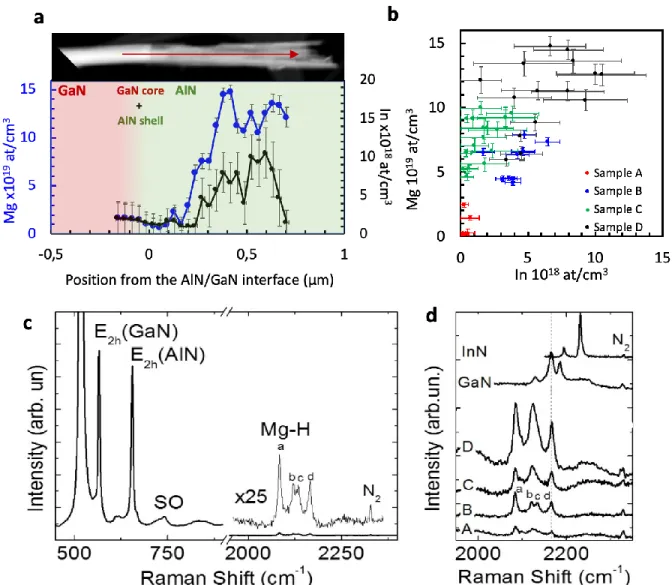
Figure 1. (a) TEM picture of dispersed nanowire from sample D and corresponding Mg (blue axis to the left) and In (black axis to the right) profiles along the growth axis. Mg and In profiles follow the same tendency, associated to eased incorporation of Mg in presence of In atoms. Note that the axis is expressed in × 1019𝑎𝑡 /𝑐𝑚3 for Mg and × 1018𝑎𝑡 /𝑐𝑚3 for In, respectively. (b) Mg concentration with respect to In
concentration showing the correlation between Mg and In incorporation. Reference sample A shows the lowest incorporation level whereas sample D shows the highest Mg and In content, consistent with co-doping conditions. (c) Raman spectrum of sample B showing the spectral range corresponding to E2h and
Mg-H modes. The intensity of the Mg-H modes has been multiplied by 25 for clarity. (d) Detail of the spectral range corresponding to the Mg-H modes of samples A to D. GaN NW9 and InN12 bulk Mg doped
Individual AlN NWs dispersed on a transmission electron microscopy (TEM) carbon grid were analyzed by EDX for each sample. Several points along the NWs growth axis were measured in order to determine statistically both Mg and In concentrations. The results are shown in Figure 1. Mg-In profiles were plotted in Figure 1.a with respect to the position from the AlN/GaN interface on individual nanowires extracted from sample D. Mg and In profiles are found to vary along the Mg-doped part of the sample, with an increasing concentration of Mg related to an increasing In concentration. A low concentration of Mg was found also in the Si-doped part and was associated to diffusion of Mg in the sample during growth as well as to the presence of a slightly Mg-doped AlN shell around the GaN stems. This mechanism was associated in GaN Mg-doped NWs to a preferential incorporation of Mg on m-planes during growth under N-rich conditions. 9
Figure 1b is showing the Mg concentration variation as a function of In concentration for all the samples. In absence of In co-doping, such as in the case of sample A, Mg concentration was found closely above detection limit of EDX technique which is of 1x10¹⁹ Mg/cm3. Indium concentration
for sample A is residual and is found to be at most 3x10¹⁸ In/cm3, close to the In detection limit in
the EDX set-up. By contrast, in presence of an In flux, the Mg content was found to increase with increasing In concentration, up to a maximum value of around 1.5x10²⁰ Mg/cm3 in sample D,
related to an In content below 1x10¹⁹ In/cm3. The concentration of In in these samples, though
higher than in sample A, is still one order of magnitude smaller than that of Mg. Results shown in figure 1.b establish a clear correlation between the incorporation of Mg and the presence of In.
Given the low In concentration (<0.01%), the formation of an AlInN ternary alloy can be safely discarded. These results were also confirmed by Raman spectroscopy.
Figure 1c shows the Raman spectrum of sample B. The E2h phonon mode characteristic of the
Additionally, the surface optical mode (SO) ascribed to GaN NWs appears as a distinctive feature. At the high frequency range and around 200 cm-1 below the stretching mode of the nitrogen
molecules from the air, four much weaker peaks are identified, labeled a, b, c and d. These are assigned to Mg-H complexes. This spectral region is shown in more detail in Figure 1d for samples A to D. The spectra of this figure have been normalized to the intensity of the E2h mode of AlN.
Consequently, the intensity of the Mg-H modes reflects the Mg content of the samples. The smallest Mg content is found in sample A, where no In co-doping has been used. The highest Mg content is displayed by sample D, doped with the highest Mg and In cell temperatures. For the sake of comparison, a reference spectrum corresponding to Mg doped GaN and InN have also been included. The frequencies of modes a (2185 cm-1), b (2123 cm-1), c (2135 cm-1) and d (2166 cm-1)
are the same for all samples, and their relative intensities remain similar. The main difference concerns peak b: its intensity is larger in samples C and D, the samples with the highest Mg and In contents. This is an indication that the configuration of Mg and H atoms changes when doping increases. Since they correspond to local modes, Mg-H vibrations are not expected to be very sensitive to the characteristics of the host lattice. However, comparison with Mg doped GaN indicates that in AlN most of the local modes appear at a smaller wave number. Interestingly, peak d is shared in both samples, indicating a common configuration of Mg and H in both lattices. The Raman spectrum of Mg doped InN is shown at the top, with two Mg-H related peaks shifted to higher frequency when compared to AlN and GaN. It is obvious that the In content of our samples is too small to detect any Mg-H mode related to InN.
To explain the improvement of Mg incorporation when AlN is In co-doped, we have investigated by means of ab initio calculations various scenarios. Calculations were performed with BigDFT 13
in orthorhombic 3D supercells containing 360 Al and N atoms in wurtzite structure. Such super-cells are large enough to compute the wavefunctions at Γ point only. The exchange and correlation
potential was defined by the Perdew-Burke-Ernzerhof (PBE) approximation14 and core electrons
were described by pseudo-potential formalism using the Hartwigsen-Goedecker-Hutter15
formulation. Since PBE is under-estimating the gap of AlN, our results are providing trends but cannot be taken quantitatively (AlN gap is found to be 4.1 eV in our PBE calculations, while it is experimentally observed around 6.2 eV). Two hypotheses can be postulated regarding the increase of Mg incorporation during growth in the presence of In. Firstly, it may be due to a direct electronic or elastic interaction between the two elements. Purely elastic effect can easily be discarded since both atoms have a positive formation volume, i.e. are both creating compressive stress into the AlN matrix, which cannot be mutually compensated. In order to test the possibility of a direct electronic interaction favouring Mg incorporation in presence of In, various situations involving substitutional In and Mg positions on the Al sub-lattice, including 1st and 2nd neighbors along the
c-axis or in the [100] and [110] directions have been calculated. However, no significant binding energies between the two elements have been found so that the hypothesis of an increased Mg incorporation mediated by a favourable electronic interaction with In can also be discarded. The alternative possibility of an indirect inter-play between the two elements, mediated by a third party has then been considered.
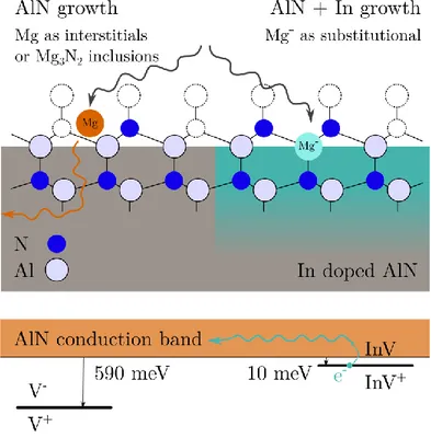
Figure 2. Better Mg incorporation in AlN in presence of indium. The InV complex is a shallow donor, easily sending an electron in the conduction band. The resulting ionization of an Mg atom is expected to ease Mg
-incorporation in Al-substitutional site in the wurtzite structure.
Such a scenario is depicted on Figure 2 and relies on the ionization of Mg atom into Mg- during
the growth process, followed by its eased incorporation in Al-substitutional site. We have considered a self-defect of AlN with a negative volume of formation to compensate for the elastic deformation induced by both In or Mg, namely the nitrogen vacancy VN. Various charge states for
different elements and complexes have been calculated. The most interesting complex, though, is the InVN one, made of a substitutional In atom with a N vacancy as 1st neighbor along the c-axis.
This is a very shallow donor, located 10 meV below the conduction band, leading to a Mg incorporation scenario along the following lines: In atoms are incorporated during growth and soon trap a N vacancy to accommodate the related elastic deformation. The InVN complex is then
Figure 2). Incoming Mg atoms can be ionized into Mg- with the electrons available from the CB.
The electronic structure of Mg- is closer to the one of Al than neutral Mg, easing its incorporation
in substitutional site in the growing wurtzite structure. By contrast, neutral or positively charged Mg tends to form Mg3N2 inclusions or interstitials Mg16 . The latter, being highly mobile, are
expected to diffuse at the nanowire edges as recently demonstrated by atom probe9.
It has to be stressed that VN alone is a deep donor located at 590 meV under the conduction band
(see left hand side in Figure 2), preventing it to efficiently ionize Mg. This highlights the specific role of InVN complexes as donors, while the nitrogen vacancy alone if indium is absent, cannot
significantly contribute to ionize Mg atoms. However, it has to be pointed out that the above calculations are performed at thermodynamic equilibrium and do not consider the kinetics of In-VN complex formation. In particular, the interaction between the surface VN reservoir and
substitutional In is expected to depend on the local density of reacting species. As a consequence, the resulting Mg/In co-doping ratio should depend not only on Mg and In fluxes but also on the AlN NW growth rate. The In-VN donors at the end of the growth process could compensate the
substitutional Mg acceptors. However, because the In-VN complexes concentration is expected to
be lower than the substitutional Mg acceptor concentration (the atomic concentration of In being at least 10 times lower than the Mg concentration), the compensation should remain partial and the In-VN contribution is beneficial as a whole for the hole conduction in the p-type region
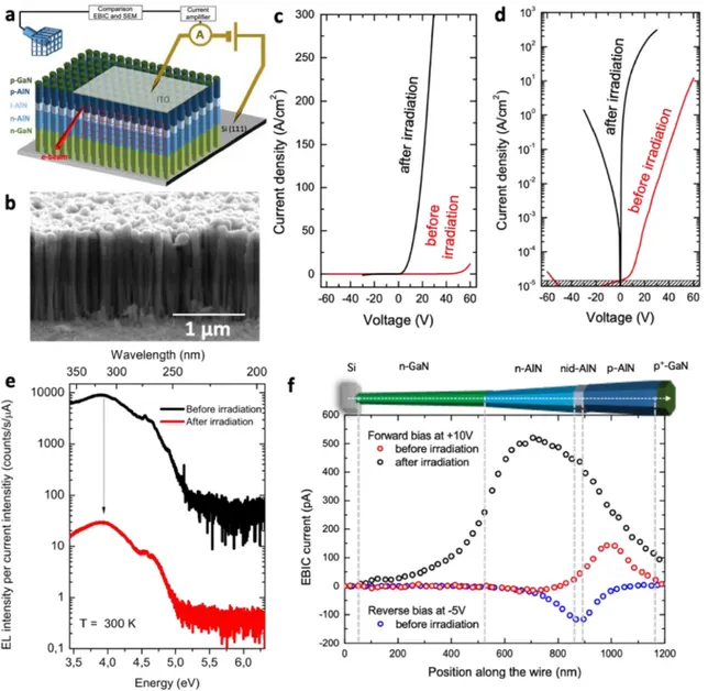
Figure 3. p-i-n diode characteristics and electrical p-type activation. (a) Schematics of the AlN p-i-n junction nanowire structure and experimental setup for electrical measurements. (b) SEM image of side-view contacted nanowires. Total length of nanowires is of approximately 1.2µm. (c) and (d) J-V characteristics of the p-i-n junction prior (red) and after (black) e-beam irradiation on a linear scale and semi-log scale, respectively. (e) Electroluminescence spectrum of sample E recorded before and after irradiation showing deep-defect emission within p-type AlN. f) SEM image and corresponding electron beam induced current (EBIC) profile measured along the dashed line of the image. The EBIC profiles have been performed before irradiation under reverse (-5V) and forward (+10V) bias regime.
Further electrical characterization was performed on sample E in order to assess the electrical activity of Mg. Figure 3a shows the schematic of the AlN p-i-n junction nanowire structure and the experimental setup for electrical measurements. The n-type GaN stem of the wire is approximately 600 nm long. Then, the AlN p-i-n junction is composed by 30 nm of undoped AlN sandwiched between n-type and p-type AlN sections of approximately 300 and 250 nm length, respectively. To ensure an efficient ohmic contact, a few nanometers thick highly doped p-type GaN (Mg content larger than 1019cm−3) was grown on top of the p-type AlN. 100 nm thick ITO ohmic contacts
were deposited directly on top of as-grown NWs of sample E. I-V measurements have been performed on 100x100 µm2 metal contacts in the SEM chamber thanks to nanomanipulators and
tungsten tips under vacuum. The voltage bias was applied on the top side contact while the backside contact was taken directly on the Si (111) substrate. Side-view contacted nanowires SEM image is shown in figure 3 b.
The current density J of the diode has been calculated by considering a filling factor of 80 %, as determined during experiments from top view SEM image. Typical J-V characteristics of the p-i-n jup-i-nctiop-i-n are reported ip-i-n Figure 3c ap-i-nd d with a lip-i-near scale ap-i-nd semi-log scale, respectively. J-V characteristics were observed to vary under e-beam irradiation. In the following, we will define “before irradiation”, the structures that have been exposed to an electron beam dose below 5mC/cm2 and “after irradiation”, the structures that have been exposed to an electron beam dose
above 3 C/cm2. To study the effect of the irradiation on a large surface, we irradiated the 100 by
100 m2 diode surface with an e-beam perpendicular to the sample surface The J-V characteristics
are rectifying whatever the e-beam irradiated dose.
Before irradiation, the current density of the diode exhibits a power law dependence versus voltage 𝐽~𝑉𝛼 in the forward regime, for voltage larger than 10 V. The 𝛼 value is estimated such
as 6 < 𝛼 < 12 depending on the diode. Such strong current increase versus voltage is generally observed in insulating semiconductors where multiplication mechanism occurs by impact ionization17. Assuming that the applied voltage holds on the most resistive 250 nm p-type part
(discussed below), the electric field can be evaluated between 0.5 and 2.4 MV/cm for V ranging between 10 V and 60 V, which are typical electric fields for impact ionization. Similar behavior under high electric fields has been shown in a p-i-n AlN structure by Taniyasu1 and is compatible
with J-V characteristics of a p-i-n AlN NW diode in the more recent article of Zhao et al18. In the
latter publication, the thin p-part of the p-i-n AlN junction of 15nm withstands large electric fields similar with that studied hereby. The reverse current density is below the detection limit (dashed area of the Figure 3 d) up to 50 V.
After e-beam irradiation, even if the rectifying behavior is maintained, the J-V plot shows a tunnel transport regime at the junction with current density much higher than before irradiation. An ohmic regime is observed in forward regime for bias voltage higher than 25V. In order to check the influence of the electron beam irradiation on the NW properties, electron beam induced current measurements (EBIC) have been done on single NWs.
To check the presence of electric field within the p-i-n junction, we performed EBIC profiles along a single NW before and after irradiation under forward and reverse bias voltage. In that specific case, the irradiation was performed using an e-beam configuration parallel to the sample surface in order to study NWs at the edge of the cleaved sample.
Observation conditions were chosen such as the e-beam irradiation dose is below the range defined previously. An electric field appears at the p-i-n junction of the sample under reverse bias (shown at –5V in Figure 3 f). Charge carriers created inside the NW or close to the p-i-n junction are separated by the intrinsic electric field localized within the p-i-n junction. This EBIC imaging clearly shows the presence of an electric field created at the p-i-n junction of the AlN NWs with an
associated space charge region (𝑤) thinner than 120 nm including the 30 nm intrinsic part of the p-i-n structure. An effective doping Neff can thus be determined from the applied potential V:
𝑁𝑒𝑓𝑓 = √
2 × 𝜀𝐴𝑙𝑁× (𝑉𝑏𝑖− 𝑉) 𝑞 × 𝑤
Where Vbi is the built-in potential, 𝜀𝐴𝑙𝑁 is the dielectric constant of AlN, q is the electric charge
and w the space charge region width. The effective doping of the NW is estimated to be higher or equal to 5×1017cm-3, indicating the presence of a highly p-doped and highly n-doped regions. In
order to check the presence of charge carriers within the structure, we performed EBIC measurement under forward regime. Prior to e-beam irradiation, the EBIC signal in forward regime appears only and systematically in the p-type AlN part of the junction indicating that the voltage drop occurs in the p-type part which is more resistive than the n-type. Also, we assign the insulating behaviour of the J-V characteristics in forward regime before irradiation to a low carrier concentration in the p-type region. Indeed, Taniyasu et al1 reported that Mg is a deep acceptor with
an ionization energy of 630 meV. In their epilayer, they measured a hole concentration of around 1011 cm-3 for a doping level in the range of 2×1019 cm-3. If we assume this hole density in the 250
nm long p-type part of the NW with an average radius of 50 nm, the equivalent number of holes in one NW is 1.5 × 10⁻⁴. This is equivalent to 200 holes in the volume corresponding to 250 nm long
p-type AlN NW section of a 100 µm × 100 µm diode. With the same assumptions, for the highest Mg concentration measured in this work by EDX, Nd, of 1.5 × 1020cm-3, the mean distance
between dopants, R, can be estimated to be 𝑅 = ( 3
4𝜋𝑁𝑑)
1/3, roughly equal to 2 nm, suggesting that
the electrical conductivity in the AlN NW section is indeed governed by hole hopping. After e-beam irradiation, EBIC signal in forward regime appears to be larger in the n-type AlN part of the
sample (Figure 3f), indicating that the p-type part became more conducting than the n-type. EBIC images at zero bias voltage are discussed in the Supplementary Information.
The scenario accounting for the increase of the conductivity following irradiation is indeed not clear. As a matter of fact, the dissociation of Mg−H complex appears as one of the possibilities, similar to the case of metal organic chemical vapor deposition (MOCVD)-grown GaN-Mg epilayers. However, the specificity of NW geometry should be considered: the electron irradiation could affect the near surface band bending or surface Fermi level pinning and accordingly change the core conductivity. This should be particularly important for AlN nanowires with diameter ranging from 75 to 100 nm.
Electroluminescence (EL) data shown in figure 3e put in evidence a drastic drop of EL intensity after e-beam irradiation. The relatively high EL intensity before e-beam irradiation, i.e. before Mg dopant activation, is consistent with the above-mentioned multiplication mechanism resulting from impact ionization. However, following Mg doping activation, the drop in EL intensity is consistent with the shift from a highly resistive regime in the p-AlN NW section to a highly conductive one and current tunneling through the p-n junction, drastically decreasing the radiative recombination probability.
The issue of efficient p-type doping of nitride semiconductors has been a subject of sustained interest for a long time. A compilation of literature results has led S. Brochen et al to conclude that the ionization energy of Mg substitutional to Ga in the low dopant concentration limit was 245 ±25 meV8. Such a high value implies to introduce large quantities of Mg to reach significant hole
concentrations at room temperature. However, the solubility of Mg in GaN layers is limited to about 1020/cm3 19. Above this concentration, Mg clustering associated with the formation of
pyramidal extended defects and partial polarity inversion has been observed20, leading to a marked
has been proposed, in order to improve the surface morphology and decrease the amount of electrically compensating point defects21. Remarkably, it has been shown by Brochen and
co-workers that the ionization energy of Mg decreased strongly as a function of the Mg content, a feature assigned to a shift from isolated impurity regime to a defect energy band at high Mg concentrations.
Besides the morphology improvement resulting from the use of In surfactant, it has been recently shown that In and Mg co-doping in GaN results in a decrease of the acceptor ionization energy, related to the changes in the valence band maximum energy in the vicinity of In-N complexes22.
Considering Mg doping of AlN, an acceptor activation energy of 630 meV has been reported by Taniyasu and co-workers1, consistent with a theoretically predicted value in the 465–758 meV
range23 and making significant hole concentration even more difficult to obtain than in GaN.
In such a context, the dramatic increase in Mg content in Mg/In codoped AlN NWs reported in the present work could be favourable to a reduction of the acceptor ionization energy similarly to the behaviour of GaN layers. This is supported by the fact that the maximum Mg doping level in presence of In, namely 1.5 × 10²⁰ Mg/cm3, is almost one order of magnitude higher than the Mg
level reported by Taniyasu [12], suggesting the formation of a band of defects and a decrease of the effective ionization energy. Regardless of the ionization energy, either 630 meV corresponding to isolated impurities or lower, the high density of Mg dopants further supports a hopping mechanism. Such a mechanism has been observed in the case of Mg-doped GaN in the 4 × 10¹⁹
-2 × 1020 cm-3 range, simultaneously with the decrease of effective Mg ionization energy24. In such
analysis, it is supposed that Mg dopants are homogeneously distributed in the matrix. However, this is not necessarily the case for NWs. As a matter of fact, it has been found that GaN NWs obeyed a specific doping regime, with a Si solubility limit higher than in layers25 and an
case of InN NWs, first principle calculation have demonstrated that the formation energy of substitutional Mg is lowered close to the surface, which has been assigned to an eased elastic strain relaxation related to the large amount of free surface in NWs27. A similar mechanism has been
invoked to account for the high p-type doping level achieved in AlN NWs11, which could be a
general feature for nitride NWs grown by plasma-assisted MBE, with a typical diameter in the 70-100 nm range. Spatial inhomogeneity in the doping of NWs, in particular the tendency to peripheral accumulation of dopants is making likely the occurrence of the above discussed related features. In the case of AlN reported here the observation of Raman modes assigned to the presence of Mg-H complexes suggest that the Mg incorporation mechanism could be similar to the case of GaN NWs and possibly favoured along the AlN NW sidewalls. Combined to a decreased formation energy and the dramatic enhancement of Mg content experimentally observed in In co-doping conditions, it appears that AlN NW morphology is extremely favourable to high Mg content incorporation. It is likely that such a high Mg content is responsible for a shift from isolated impurity regime towards a regime dominated by the formation of a defect band and a marked decrease of the effective dopant ionization energy leading to a significant p-type conduction.
Methods
Samples manufacture
AlN NW samples were grown by PA-MBE in a MECA2000 machine. NWs were grown along the c-axis on a low resistivity 2” Si (111) wafer, n-type doped with As. The substrates were cleaned prior to growth in a 10% HF solution for 45s and annealed at 900°C for 30 min in the MBE chamber. The substrate temperature is monitored by using a thermocouple in contact with the rear face of the molybdenum substrate holder. The fluxes were calibrated from equivalent growth rates determined by reflection high-energy electron diffraction (RHEED) oscillations on GaN and AlN
templates. A series of AlN p-n junction samples (noted A, B, C and D in table 1) were grown on Si-doped GaN stems to ensure the electrical conductivity with respect to the substrate. Nitrogen rich conditions with a plasma cell radio frequency power of 600W and a N2 flux of 2.5 sccm were
chosen for all the samples, corresponding to a GaN growth rate of 1 ML/s in N limited regime. GaN NW stems were grown at a Ga/active N nominal flux ratio of 0.3. For n-type doping of the stems, a temperature of 900°C was set for the Si effusion cell. Substrate temperature was maintained constant throughout the growth of n-type part at 800°C. AlN part was grown at a constant Al/active N nominal flux ratio of 0.15. n-type part was grown directly on the stems with a Si-doping cell temperature of 900°C. p-type doping growth parameters, mainly Mg and In fluxes, were varied during growth of the AlN p-part of the sample in order to have a complete study of co-doping conditions. Indium cell temperature was varied from 700°C to 800°C and magnesium cell temperature was varied from 280°C up to 300°C, as summarized in Table 1.
A reference sample (sample A) was grown at a Mg effusion cell temperature of 280°C without In assistance, but keeping the same growth parameters otherwise. Other growth parameters were constant unless otherwise specified.
In order to assess the electrical properties of the NWs, an AlN NW p-i-n junction with an undoped active region of 30 nm was grown with optimized growth conditions (Sample E). Si doping temperature for GaN and AlN NW sections was 920°C and 1000°C, respectively. p-type AlN NW part of the junction was grown at Mg and In cell temperatures of 280 and 800°C, respectively. The structure was eventually capped with a heavily p-type doped GaN section, 20 nm thick, at a Mg doping cell temperature of 280°C, in order to assure a good ohmic contact for electrical characterization purposes.
p-type ohmic contacts and remove the residual resist on the surface of the nanowires, sample E was exposed to O2 plasma prior to metal deposition. The thickness of the ITO contact layer deposited
by physical vapor deposition (PVD) sputtering was 100 nm. The contacts were annealed at 550°C during 5 min in N2 atmosphere. Samples were cleaved in order to have access to as-grown contacted
nanowires.
Measurements
Energy Dispersive X-ray (EDX) Spectroscopy was performed on a probe corrected FEI Titan Themis equipped with four windowless silicon drift detectors. X-ray spectra were acquired during 1-5 minutes at 200 kV with high probe currents (from 3.5 up to 7.8 nA) to increase the counting statistics (> 100 kcps) and thus to lower the detection limit for Mg and In in AlN down to 1 − 5 × 10¹⁸ 𝑎𝑡/𝑐𝑚3. The net intensities of N K-line (K: 0.39 keV), Al K-lines (K: 1.49 keV; K: 1.56
keV) and Ga K-lines (K: 9.23-9.25 keV; L: 10.26-10.35 keV) were extracted from the X-ray spectra using the QUANTAX-800 software from BRUKER. The net intensities of Mg K-line (K: 1.25 keV) and In L-lines (L: 3.28 keV; L: 3.49-3.79 keV; L: 3.82-4.16 keV; Ll,e: 2.91-3.11 keV) in AlN were extracted by normalizing X-ray spectra to a pure AlN reference spectrum acquired in the same conditions. The conversion of the net X-ray intensities into concentrations was performed using the zeta-factor method allowing correcting intensities from X-ray absorption28. The zeta-factors were directly measured on the same equipment, at the same operating
conditions, using reference samples of known composition and thickness29.
Raman spectroscopy experiments were performed in backscattering configuration using the 532 nm line of a laser diode as excitation source. A Horiba Jobin Yvon Xplora spectrometer equipped with a Peltier-cooled charge coupled device detector and 1800 grooves/mm diffraction gratings
was used for spectral analysis. A 100x microscope objective focused the excitation laser on the sample and collected the backscattered light to the spectrometer.
Contacting for electrical characterization was done directly in a FEI Inspect F50 scanning electron microscope (SEM) using tungsten tips. 500 nm radius tips were cleaned by SF6 plasma
and a high voltage was applied prior to contacting in order to get rid of the oxide and get a better contacting surface. A voltage source was used to apply a bias on the top side contact while backside contact was taken directly on the Si (111) substrate.
In order to visualize and characterize the p-n junction in the AlN NW, EBIC measurements have been performed in field emission gun scanning electron microscope (FEI Inspect F50 SEM), with a beam energy of 10kV and a current of 30 pA, in order to maintain the spatial resolution. Casino simulations show that interaction pear dimensions are of around 100 nm corresponding to the first row of nanowires.
Electroluminescence experiments were performed at T = 300 K in a FEI Inspect F50 SEM. A Horiba Jobin Yvon ihR 550 spectrometer equipped with a Peltier-cooled charge coupled device detector and a 600 grooves/mm diffraction grating was used for spectral analysis. The electrical injection was carried out using nanomanipulators.
AUTHOR INFORMATION
Corresponding Author
*[email protected] OR [email protected] [email protected]
Funding Sources
This work has been partially supported by Agence Nationale de la Recherche (EMOUVAN project-ANR-15-CE24-0006- 04). A. C. and N. G. acknowledge financial support from project ENE2016-79282-C5-3-R from the Spanish MICINN and PROMETEO/2018/123 from Generalitat Valenciana.
Notes
The authors declare no competing financial interest. ACKNOWLEDGMENT
The authors would like to thank Yann Genuist and Yoan Curé from CEA Grenoble for technical support during MBE growth, the Nanofab team at Neel Institute for the use of their facilities and technical assistance.
ABBREVIATIONS
MBE, molecular beam epitaxy; LED, light emitting diodes; NW, nanowires; SEM, scanning electron microscopy; EDXS, energy dispersive X-Ray spectroscopy; PA-MBE, plasma assisted molecular beam epitaxy; SCCM, standard cubic centimeters per minute;
REFERENCES
(1) Taniyasu, Y.; Kasu, M.; Makimoto, T. An Aluminium Nitride Light-Emitting Diode with a Wavelength of 210 Nanometres. Nature 2006, 441 (7091), 325–328. https://doi.org/10.1038/nature04760.
(2) Takano, T.; Mino, T.; Sakai, J.; Noguchi, N.; Tsubaki, K.; Hirayama, H. Deep-Ultraviolet Light-Emitting Diodes with External Quantum Efficiency Higher than 20% at 275 Nm Achieved by Improving Light-Extraction Efficiency. Appl. Phys. Express 2017, 10 (3), 031002. https://doi.org/10.7567/APEX.10.031002.
(3) Sanchez-Garcia, M. A.; Calleja, E.; Monroy, E.; Sanchez, F. J.; Calle, F.; Muñoz, E.; Beresford, R. The Effect of the III/V Ratio and Substrate Temperature on the Morphology and Properties of GaN- and AlN-Layers Grown by Molecular Beam Epitaxy on Si(1 1 1). J. Cryst. Growth 1998, 183 (1), 23–30. https://doi.org/10.1016/S0022-0248(97)00386-2. (4) Yoshizawa, M.; Kikuchi, A.; Mori, M.; Fujita, N.; Kishino, K. Growth of Self-Organized GaN
Nanostructures on Al2O3(0001) by RF-Radical Source Molecular Beam Epitaxy. Jpn. J. Appl. Phys. 1997, 36 (4B), L459. https://doi.org/10.1143/JJAP.36.L459.
(5) Sánchez-Páramo, J.; Calleja, J. M.; Sánchez-Garcia, M. A.; Calleja, E. Optical Investigation of Strain in Si-Doped GaN Films. Appl. Phys. Lett. 2001, 78 (26), 4124–4126. https://doi.org/10.1063/1.1379063.
(6) Neugebauer, J. Surfactants and Antisurfactants on Group-III-Nitride Surfaces. Phys. Status Solidi C 2003, 0 (6), 1651–1667. https://doi.org/10.1002/pssc.200303132.
(7) Fang, Z.; Donatini, F.; Daudin, B.; Pernot, J. Axial p–n Junction and Space Charge Limited Current in Single GaN Nanowire. Nanotechnology 2018, 29 (1), 01LT01. https://doi.org/10.1088/1361-6528/aa9a0e.
(8) Brochen, S.; Brault, J.; Chenot, S.; Dussaigne, A.; Leroux, M.; Damilano, B. Dependence of the Mg-Related Acceptor Ionization Energy with the Acceptor Concentration in p-Type GaN Layers Grown by Molecular Beam Epitaxy. Appl. Phys. Lett. 2013, 103 (3), 032102. https://doi.org/10.1063/1.4813598.
(9) Siladie, A.-M.; Amichi, L.; Mollard, N.; Mouton, I.; Bonef, B.; Catherine Bougerol; Grenier, A.; Robin, E.; Jouneau, P.-H.; Garro, N.; et al. Dopant Radial Inhomogeneity in Mg-Doped GaN Nanowires. Nanotechnology 2018, 29 (25), 255706. https://doi.org/10.1088/1361-6528/aabbd6.
(10) Zhao, S.; Mi, Z. Al(Ga)N Nanowire Deep Ultraviolet Optoelectronics. Semicond. Semimet. 2017, 96, 167–199. https://doi.org/10.1016/bs.semsem.2016.05.001.
(11) Zhao, S.; Connie, A. T.; Dastjerdi, M. H. T.; Kong, X. H.; Wang, Q.; Djavid, M.; Sadaf, S.; Liu, X. D.; Shih, I.; Guo, H.; et al. Aluminum Nitride Nanowire Light Emitting Diodes: Breaking the Fundamental Bottleneck of Deep Ultraviolet Light Sources. Sci. Rep. 2015, 5, srep08332. https://doi.org/10.1038/srep08332.
(12) Cuscó, R.; Domènech-Amador, N.; Artús, L.; Wang, K.; Yamaguchi, T.; Nanishi, Y. Temperature Dependence of Mg-H Local Vibrational Modes in Heavily Doped InN:Mg. J. Appl. Phys. 2012, 112 (5), 053528. https://doi.org/10.1063/1.4749266.
(13) Genovese, L.; Neelov, A.; Goedecker, S.; Deutsch, T.; Ghasemi, S. A.; Willand, A.; Caliste, D.; Zilberberg, O.; Rayson, M.; Bergman, A.; et al. Daubechies Wavelets as a Basis Set for Density Functional Pseudopotential Calculations. J. Chem. Phys. 2008, 129 (1), 014109. https://doi.org/10.1063/1.2949547.
(14) Perdew, J. P. Generalized Gradient Approximation Made Simple. Phys. Rev. Lett. 1996, 77 (18), 3865–3868. https://doi.org/10.1103/PhysRevLett.77.3865.
(15) Hartwigsen, C.; Goedecker, S.; Hutter, J. Relativistic Separable Dual-Space Gaussian Pseudopotentials from H to Rn. Phys. Rev. B 1998, 58 (7), 3641–3662. https://doi.org/10.1103/PhysRevB.58.3641.
(16) Miceli, G.; Pasquarello, A. Self-Compensation Due to Point Defects in Mg-Doped GaN. Phys. Rev. B 2016, 93 (16), 165207. https://doi.org/10.1103/PhysRevB.93.165207.
(17) Baliga, B. J. Fundamentals of Power Semiconductor Devices; Springer: New York, NY, 2008.
(18) Zhao, S.; Djavid, M.; Mi, Z. Surface Emitting, High Efficiency Near-Vacuum Ultraviolet Light Source with Aluminum Nitride Nanowires Monolithically Grown on Silicon. Nano Lett. 2015, 15 (10), 7006–7009. https://doi.org/10.1021/acs.nanolett.5b03040.
(19) Namkoong, G.; Doolittle, W. A.; Brown, A. S. Incorporation of Mg in GaN Grown by Plasma-Assisted Molecular Beam Epitaxy. Appl. Phys. Lett. 2000, 77 (26), 4386–4388. https://doi.org/10.1063/1.1334942.
(20) Vennéguès, P.; Benaissa, M.; Dalmasso, S.; Leroux, M.; Feltin, E.; De Mierry, P.; Beaumont, B.; Damilano, B.; Grandjean, N.; Gibart, P. Influence of High Mg Doping on the Microstructural and Optoelectronic Properties of GaN. Mater. Sci. Eng. B 2002, 93 (1), 224– 228. https://doi.org/10.1016/S0921-5107(02)00046-6.
(21) Kyle, E. C. H.; Kaun, S. W.; Young, E. C.; Speck, J. S. Increased P-Type Conductivity through Use of an Indium Surfactant in the Growth of Mg-Doped GaN. Appl. Phys. Lett. 2015, 106 (22), 222103. https://doi.org/10.1063/1.4922216.
(22) Liu, Z.; Fu, B.; Yi, X.; Yuan, G.; Wang, J.; Li, J.; Luna; Ferguson, I. Co-Doping of Magnesium with Indium in Nitrides: First Principle Calculation and Experiment. RSC Adv. 2016, 6 (6), 5111–5115. https://doi.org/10.1039/C5RA24642C.
(23) Mireles, F.; Ulloa, S. E. Acceptor Binding Energies in GaN and AlN. Phys. Rev. B 1998, 58 (7), 3879–3887. https://doi.org/10.1103/PhysRevB.58.3879.
(24) Kozodoy, P.; Xing, H.; DenBaars, S. P.; Mishra, U. K.; Saxler, A.; Perrin, R.; Elhamri, S.; Mitchel, W. C. Heavy Doping Effects in Mg-Doped GaN. J. Appl. Phys. 2000, 87 (4), 1832– 1835. https://doi.org/10.1063/1.372098.
(25) Fang, Z.; Robin, E.; Rozas-Jiménez, E.; Cros, A.; Donatini, F.; Mollard, N.; Pernot, J.; Daudin, B. Si Donor Incorporation in GaN Nanowires. Nano Lett. 2015, 15 (10), 6794– 6801. https://doi.org/10.1021/acs.nanolett.5b02634.
(26) Northrup, J. E. Hydrogen and Magnesium Incorporation on C-Plane and m-Plane GaN Surfaces. Phys. Rev. B 2008, 77 (4), 045313. https://doi.org/10.1103/PhysRevB.77.045313. (27) Zhao, S.; Le, B. H.; Liu, D. P.; Liu, X. D.; Kibria, M. G.; Szkopek, T.; Guo, H.; Mi, Z.
P-Type InN Nanowires. Nano Lett. 2013, 13 (11), 5509–5513. https://doi.org/10.1021/nl4030819.
(28) Watanabe, M.; Williams, D. B. The Quantitative Analysis of Thin Specimens: A Review of Progress from the Cliff-Lorimer to the New ζ-Factor Methods. J. Microsc. 2006, 221 (2), 89–109. https://doi.org/10.1111/j.1365-2818.2006.01549.x.
(29) Lopez-Haro, M.; Bayle-Guillemaud, P.; Mollard, N.; SaintAntonin, F.; Van Vilsteren, C.; Freitag, B.; Robin, E. Obtaining an Accurate Quantification of Light Elements by EDX: K-Factors vs. Zeta-K-Factors. In 18th International Microscopy Congress Czechoslovak Microscopy Society; Prague, 2014.