HAL Id: hal-01760595
https://hal.archives-ouvertes.fr/hal-01760595
Submitted on 29 Jul 2020
HAL is a multi-disciplinary open access archive for the deposit and dissemination of sci-entific research documents, whether they are pub-lished or not. The documents may come from teaching and research institutions in France or abroad, or from public or private research centers.
L’archive ouverte pluridisciplinaire HAL, est destinée au dépôt et à la diffusion de documents scientifiques de niveau recherche, publiés ou non, émanant des établissements d’enseignement et de recherche français ou étrangers, des laboratoires publics ou privés.
Experimental study to push the Flash floating gate
memories toward low energy applications
V. Della Marca, A. Regnier, J. Ogier, R. Simola, S. Niel, J. Postel-Pellerin, F.
Lalande, G. Molas
To cite this version:
V. Della Marca, A. Regnier, J. Ogier, R. Simola, S. Niel, et al.. Experimental study to push the Flash floating gate memories toward low energy applications. 2011 International Semiconductor Device Research Symposium (ISDRS), Dec 2011, College Park, France. pp.73 - 77, �10.1109/IS-DRS.2011.6135271�. �hal-01760595�
ISDRS 2011, December 7-9, 2011, College Park, MD, USA
ISDRS 2011 – http://www.ece.umd.edu/ISDRS2011
Student Paper
Experimental Study to Push the Flash Floating Gate Memories Toward Low Energy
Applications
V. Della Marcaa,b,c, A.Regniera, J.-L. Ogiera, R. Simolaa, S. Niela, J. Postel-Pellerinb, F. Lalandeb, and G. Molasc
a
STMicroelectronics, Rousset, France, [email protected], b Aix-Marseille University, IM2NP, CNRS, France,
c CEA-LETI, Grenoble, France.
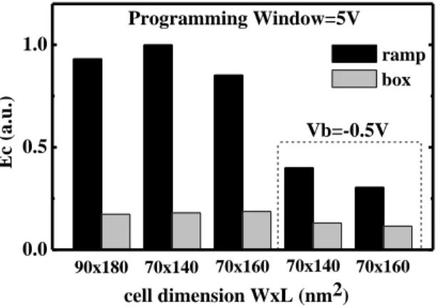
The problem of energy saving has today a relevant importance, concerning in particular all the portable devices as smart phone, tablet PC, smart card and so on [1]. In order to improve the features of these products, particular attention is paid to energy consumption of Flash cells in memory arrays. In this work we investigated the Flash floating gate (FG) dynamic behavior during the channel hot electron (CHE) programming operation. After this, we propose a solution to optimize the energy consumption. The samples studied in this experimental work are Flash floating gate memory cells (embedded NOR flash process). The ONO inter-poly dielectric stack has an equivalent thickness of 14nm, while the tunnel oxide of 9.5nm is grown on a p-type silicon substrate. The width and length channel dimensions are varied as well as the channel doping dose (CDD) and the lightly doped drain (LDD) energy implantation. In Fig. 1 we show the effect of ramp (a) and box (b) gate pulses on the programming window (PW) and energy consumption (Ec). The experimental setup and the method to calculate the energy are shown in [2]. Using a box is possible to obtain a good window saving the energy and the programming time (tp), in despite of the drain current peak at the pulse beginning [3]. We performed the same experiments on the samples with different dimensions: (90x180)nm2, (70x160)nm2 and (70x140)nm2. Several tests are performed using the reverse body bias (Vb=-0.5V) with fixed drain potential (Vd=3.8V) to demonstrate that it is possible to optimize the programming pulse, minimizing the Ec if the PW=5V is kept constant (Fig. 2). The drain current (Id) peak can disturb the control circuits of memory array [4]; to avoid this we decided to use a ramp followed by a plateau in order to characterize the devices.
The channel doping dose is a parameter that plays an important role concerning the drain current consumption during a CHE injection. In Fig. 3 we show the effect of channel doping dose variation during the programming operation. The results report the improvement of programming window and consumption energy if the CDD is increased. The channel doping dose variation produces also the threshold voltage shift [5], in this case an adjusting of sense circuits is needed for an industrialization contest. The gate voltage pulse (Vg) used to measure the Id is obtained adding the 1.5V/µs ramp and a 1µs plateau (inset of Fig. 3), the drain voltage is constant (Vd=3.8V).
An important point to evaluate, for a NOR architecture memory array, is the bitline leakage (BLL), due to a Gate Induced Drain Leakage (GIDL) in band-to-band tunneling (BBT) regime, during the CHE programming operation [6, 7]. We performed the measurements on a cell where the control gate and the floating gate are short-circuited; all the geometrical parameters are kept constant. The gate terminal is biased with -3V, the drain with 3.8V and the body using -0.5V. This condition allows to measure the Id of a non-selected programmed cell. In Fig. 4 we show that the BLL decrease if the arsenic LDD implant energy is increased. In fact, as it has been verified by process TCAD simulation (Fig. 5), increasing the LDD implant energy, the profile of drain-body junction becomes more abrupt, so the electric field in this region decreases. It is important to find the trade-off between the BLL and the programming efficiency.
In this work we investigated the effect of channel hot electron programming operation for a Flash floating gate memory cell, by ramp or by box. We have shown the gain in terms of consumed energy that is possible to reach adjusting the programming conditions and scaling the cell dimensions. Moreover we demonstrate the effect of channel doping dose to reduce the energy and improving the programming window. Concerning the implementation of a memory cell in a NOR array, a trade-off between the bitline leakage and programming current can be found engineering the lightly doped drain implantation. References
[1] L. Larcher, P. Pavan, A. Maurelli; “Flash Memories for SoC: an Overview on System Constraints and Technology Issues”;
Proc. IDEAS, pp. 73-77, July 2005.
ISDRS 2011, December 7-9, 2011, College Park, MD, USA
ISDRS 2011 – http://www.ece.umd.edu/ISDRS2011
Programming Current for Flash Memory Cell Energy Consumption Optimization”; SISC, December 2011.
[3] D. Esseni, A. Della Strada, P. Cappelletti, B. Ricco, “A new and flexible scheme for hot-electron programming of nonvolatile memory cells”, IEEE Trans. on Elec. Dev., vol. 46, pp. 125-133, January 1999.
[4] D. Munteanu, A.-M. Ionescu, “Modeling of drain current overshoot and recombination lifetime extraction in floating-body submicron SOI MOSFETs”, IEEE Trans. on Elec. Dev., vol. 49, pp. 1198-1205, July 2002.
[5] S.M. Sze, “Physics of semiconductor devices”, second edition, Wiley-Intersience publication, 1981 .
[6] S. A. Parke, J. E. Moon, H.-J. C. Wann, P. K. Ko, C. H. Hu; “Design for Suppression of Gate-Induced Drain Leakage in LDD MOSFET’s Using a Quasi-Two-Dimensional Analytical Model”; IEEE Trans. on Elec. Dev., vol. 39, pp. 1694-1703, July 1992.
[7] D. Rideau, A. Dray, F. Gilibert, F. Agut, L. Giguerre, G. Gouget, M. Minondo and A. Juge; “Characterization & Modeling of Low Electric Field Gate-Induced-Drain-Leakage”, Proc. IEEE ICMTS, vol.17, pp. 149-154, March 2004.
0.1 1 10 100 0.0 0.2 0.4 0.6 0.8 1.0 Ec PW Ramp Speed V/s) P W ( a .u .) 0.0 0.2 0.4 0.6 0.8 1.0 E c ( a .u .) (a) 0.01 0.1 1 10 0.0 0.2 0.4 0.6 0.8 1.0 Ec PW Box Duration s) P W ( a .u .) 0.0 0.2 0.4 0.6 0.8 1.0(b) E c ( a .u .)
Fig. 1 Dependence of programming window (PW) and energy consumption (Ec) from programming ramp speed(a),
and box pulse duration (b).
0.0 0.5 1.0 Vb=-0.5V Programming Window=5V 70x160 70x140 70x160 70x140 90x180 E c ( a .u .) ramp box cell dimension WxL (nm2) 1.0 1.5 2.0 2.5 0.2 0.4 0.6 0.8 1.0 Ec PW
Channel Doping Dose (a.u)
P W ( a .u .) 0.2 0.4 0.6 0.8 1.0 E c ( a .u .) 0 1 2 3 4 5 6 7 0 2 4 6 8 10 V g ( V ) time (s)
Fig. 2 Consumed energy, optimizing the
programming pulse for different geometries, when the programming window is kept constant (PW=5V).
Fig. 3 Effect of channel doping dose on programming
window (PW) and energy consumption (Ec). Inset: the gate voltage (Vg) of programming pulse.
0.0 0.2 0.4 0.6 0.8 1.0 +30 +20 +10 std B L L ( a .u .) LDD keV)
Fig.4 BitLine Leakage (BLL) vs Lightly Doped
Drain (LDD) implant energy.
Fig. 5 TCAD simulations of LDD profile using