Université Batna 2 – Mostefa Ben Boulaïd
Faculté de Technologie
Département d’Électronique
Thèse
Préparée au sein du Laboratoire d'Electronique Avancée (LEA)
Présentée pour l’obtention du diplôme de :
Doctorat en Sciences en Électronique
Option : Microélectronique
Sous le Thème :
Contribution to the modeling and optimization of nanoscale
VSG MOSFETs : Application to the nanoscale circuits
design
Présentée par :
Nidhal ABDELMALEK
Devant le jury composé de
:
M. Abdelhamid BENHAYA Prof. Université de Batna 2 Président M. Fayçal DJEFFAL Prof. Université de Batna 2 Rapporteur M. Abdesselam HOCINI Prof. Université de M'Sila Examinateur M. Djamel KHEDROUCHE Prof. Université de M'Sila Examinateur
Acknowledgements
First of all, I thank ALLAH almighty who armed me with determination, patience and courage during all these years of study.
I would like to express my sincere gratitude to my adviser, Pr. Fayçal DJEFFAL, for his solid technical guidance, continuous support and encouragement in my work and for his responsiveness to my requests.
I am also grateful to Pr. Abdesselam HOCINI and Pr. Djamel KHEDROUCHE, who accepted to be my jury members, and devoted their precious time to review my thesis. I also want to thank Pr. Abdelhamid BENHAYA for having agreed to preside this jury.
I would like to thank Dr. Toufik BENTRCIA for his orientations and his judicious advice.
Finally, my deep recognition goes to my dear parents, Abdelhamid and Farida, for all their encouragements and continuous support during this period of research. My deep recognition goes to my late beloved grandmother Fatima.
A particular gratitude to my sister Dr. Ibtissem ABDELMALEK and her Husband Pr. Nabil BENOUDJIT, for their advice, moral support and encouragements. I am also grateful to all my family, especially my brother Hachemi and my sister Ahlem. I also would like to thank my friend Hamza AZZA for his support. Once again thanks for all.
In this dissertation, a contribution to the study, modeling and reliability evaluation of advanced MOSFET devices is presented. The focus is made on two devices, identified as a potential solution for the near future scaling and integration technology, namely the tunnel and junctionless field effect transistors (TFET and JLFET). An insight on the transport physics permits a comprehensive study of the devices’ characteristics and performances.
A continuous and accurate model based on two-dimensional potential solution of an undoped tunnel transistor in vertical surrounding gate structure (VSG-TFET) is proposed. The continuity of the developed model provides the possibility to extract the analog/RF parameters and the device figures of merit (FOMs). Moreover, the role of introducing a high-κ layer on the gate oxide in improving the VSG-TFET behavior is explored for high-performance analog/RF applications. The proposed continuous analytical model can be easily implemented in commercial simulators to study and investigate VSG-TFET-based nanoelectronic circuits.
A semi-analytical model of an undoped heterojunction tunnel transistor in vertical surrounding gate structure (VSG-TFET) is developed. Basing on nonlocal approach and using an appropriate set of the wavevectors and region contribution, the tunneling current expression is derived. The model is calibrated and validated by two-dimensional numerical simulations. The impact of materials composition, dimensions and voltage supplies on the device performances is investigated and clarified. Terminal capacitances expressions complete the core model that is then used for the optimization of the device at circuit level. Design rules for heterojunction TFET based digital and analog/RF applications are outlined.
The JLFET reliability is investigated. A comparative evaluation of the hot carrier degradation (HCD) in VSG-JLFET and equivalent inversion mode device is proposed. The study focuses on the interface states creation by hot electron injection (HEI). Basing on the evolution of the interface states spatial distribution with extended stress time, and using the amphoteric property of the traps, an assessment of the aging phenomenon on various devices’ parameters is performed. The evaluation of HCD on static and dynamic operation of both device types in CMOS inverter configuration is carried out.
Keywords: Vertical surrounding-gate, Tunneling FET, Heterojunction, Junctionless FET, Continuous
Dans cette thèse, une contribution à l'étude, la modélisation et l'évaluation de la fiabilité des dispositifs MOSFETs avancés est présentée. L'effort est centré sur deux dispositifs, identifiés comme une solution potentielle pour les mise à l'échelle et technologie d'intégration dans un futur proche, à savoir les transistors à effet tunnel et sans-jonction à effet de champ (TFET et JLFET). Un aperçu de la physique des transports permet une étude complète des caractéristiques et des performances des dispositifs.
Un modèle continu et précis basé sur la solution 2-D du potentiel d’un transistor à effet tunnel non dopée dans une structure verticale à grille enrobé (VSG-TFET) est proposé. La continuité du modèle proposé offre la possibilité d'extraire les paramètres analogiques/RF ainsi que les facteurs de mérite du composant (FOM). De plus, le rôle de l'introduction d'une couche à haute permittivité dans l'oxyde de grille dans l'amélioration du comportement du VSG-TFET est exploré pour des applications analogiques/RF hautes performances. Le modèle analytique continu proposé peut être facilement implémenté dans des simulateurs commerciaux afin d’étudier et d’explorer les circuits nanoélectroniques basés sur le VSG-TFET.
Un modèle semi-analytique d'un transistor tunnel à hétérojonction non dopé dans une structure verticale à grille enrobé (VSG-TFET) est développé. L'expression du courant tunnel est dérivée en se basant sur une approche non locale et en utilisant un ensemble approprié des contributions des vecteurs d'onde et région de transmission. Le modèle est calibré et validé par des simulations numériques à deux dimensions. L'impact de la composition des matériaux, des dimensions et des tensions d'alimentation sur les performances du dispositif est étudié et clarifié. Les expressions de capacités des terminaux permettent de compléter le modèle de base, servant par la suite à optimiser le dispositif au niveau du circuit. Des règles de conception sont formulées pour les applications numériques et analogiques/RF à base de TFET à hétérojonction.
La fiabilité du JLFET est étudiée. Une évaluation comparative de la dégradation induite par les porteurs chauds (HCD) dans le VSG-JLFET et un dispositif équivalent à mode d'inversion est proposée. L'étude porte sur la création d'états d'interface par injection d'électrons à chaud (HEI). En se basant sur l'évolution de la distribution spatiale des états d'interface pour un temps de contrainte étendu, et en utilisant la propriété amphotère des pièges, une évaluation du phénomène de vieillissement sur les divers paramètres des dispositifs est effectuée. L'évaluation de la HCD sur le fonctionnement statique et dynamique des deux types de dispositifs dans une configuration d’inverseur CMOS est menée.
Mots Clés: Structure verticale à grille enrobé, Transistor à effet tunnel, hétérojonction ,Transistor sans
jonction, modèle continu, analogique/RF, Dégradation induite par les porteurs chauds, Fiabilité des circuits.
هذه ي ف ،ةحورطلأا ي ف ةمهاسم ميدقت متي ،ةسارد و ةجذمن ةيقوثوم مييقت تاينب MOSFET ا لىع تك رتلا متي .ةمدقتمل يتينب ، ددح ت ا حتلا ايجولونكتل لمتحم لحك و ميج جمدلا بيرقلا لبقتسملا ي ف تاروتسزنا رتلا امهو ، ةيلقحلا تاذ تثأت ي ر قفن ودد و ( لئاصو TFET و JLFET ت .) ةرظن حمس ةماع صئاصخل ةلماش ةسارد ءارجإب لقنلا ءاي تف ي ف تاينبلا ادأو ء .اه داعدلأا ي ئانث لح لىع مئاق قيقدو رمتسم جذومن ح رتقي لل يكيتاتسوتكللاا ع يزوتر روتسزنا رتل ذ ي تثأت ي ر قفن ودد بيوشت ي ف ةينب ةيدومع تاذ ةداوب ةيناوطسا ( VSG-TFET ناكمإ ح رتقملا جذومنلا ةيرارمتسا رفوت .) /ةيرظانتلا تاملعملا جارختسا ةي تاددرت ويدارلا ( ةرادجلا ماقرأو FOMs لىع ةولاعو .) ،كلذ ي ةيلاع ةقبط لاخدإ رود فاشكتسا مت ةيحامسلا ي ف ةداوبلا ديسكأ لىع يسحت ءادأ VSG-TFET ةيرظانتلا تاقيبطتلل / تاددرت ويدارلا ةيلاع ةيلاعفلا نكمي . إ جارد ح رتقملا رمتسملا يلىيلحتلا جذومنلا ي ف ةلوهسب تاودأ اكاحملا ة ل ةيراجتلا ل لىع دمتعت ي رتلا ةينوتكللإا ونانلا رئاود نم ققحتلا و ةساردر VSG-TFET . ي مت ريوطت جذومن هبش يلىيلحت روتسزنا رتل ذ ي تثأت ير قفن تغ سناجتم ودد بيوشت ي ف ةيدومع ةينب تاذ ةداوب ةيناوطسا ( VSG-TFET .) ادانتساً لىإ جهنلا تغ يلىحملا مادختسابو ةعومجم ةبسانم ةمهاسمل عاعش تاجوملا و نم ا قط لاا ،لاقتن متي قاقتشا تبعتلا رايتلل لا قفن . متي ةرياعم جذومنلا ققحتلاو نم هتحص ةطساوب ةاكاحم ةيمقر ةيئانث داعدلأا . متي ةسارد حيضوتو تثأت ةبيكرت داوملا داعدلأاو تامزلتسمو دهجلا لىع ءادأ ةينبلا . لمكت تباعت ةعسلا جذومنلا يساسلأا يذلا متي همادختسا دعد كلذ يوجتل د ةينبلا لىع ىوتسم دلا ةيئابرهكلا رئاو . ي مت حا رتقا دعاوق ميمصتلا نم لجأ تاقيبطتلا ةيمقرلا و ةيرظانتلا / تاددرت ويدارلا ةمئاقلا لىع TFET تغ سناجتم . ةيقوثوم ي ف قيقحتلا متي JLFET ل راقم مييقت ءارجإ متي . ل روهدت نع جتانلا ( نخاسلا لماحلا HCD ي ف ) ةينب VSG-JLFET و ةينب عضو .سوكعم زك رتت تلااح ءاشنإ لىع ةساردلا ي تيبلا حطسلا قيرط نع ( نخاسلا و رتكللإا نقح HEI لىإ دانتسلااد .) ي ئاكملا ع يزوتلا روطت ل تلااح ي تيبلا حطسلا دتما عم دا داهجلإا نمز ةيصاخلا مادختسابو ، ةدذدذملا دئاصملل مييقت ءارجإ متي ، لىع ةخوخيشلا ةرهاظل م فلتخ تاينبلا صئاصخ مييقت ءارجإ متي . HCD نم يعونلا لاكل يكيمانيدلاو تداثلا ليغشتلا لىع تاينبلا ي ف ةليكشت سكاع CMOS . تاملكلا ةلادلا : ةيدومع ةينب تاذ ةداوب ةيناوطسا ، روتسزنارت ذ و تثأت ير قفن ، ةسناجتم تغ ةلصو ، روتسزنارت لئاصو ودد ، من جذ ة رمتسم ة ، ةيرظانت / تاددرت ويدارلا ، ا ل روهدت نع جتانلا ،نخاسلا لماحلا ةيقوثوم رئاودلا .
1. Introduction and state of the art ... 1
Thesis outline ... 6
References ... 8
Chapter 2: TFET, from theory to application 2.1. Introduction ... 10
2.2. Tunneling theory ... 10
2.3. Tunneling mechanisms in semiconductors ... 12
2.4. Tunnel field effect transistor ... 18
2.4.1. Working principle ... 19
2.4.2. TFET characteristics and metrics ... 22
2.4.3. Transport mechanisms in TFET ... 26
2.4.4. Different TFET configurations ... 27
2.5. TFET enhancement ... 29 2.5.1. Geometry dependence ... 30 2.5.2. Gate engineering ... 32 2.5.3. Material engineering ... 33 2.6. Conclusion ... 36 References ... 38
Chapter 3: Semi-analytical modeling of the VSG TFET 3.1. Introduction ... 44
3.2. Current model derivation ... 45
3.3. Results and discussion ... 60
3.3.1. Analog/RF parameters ... 60
3.3.2. Linearity analysis ... 63
3.4. Conclusion ... 67
References ... 68
Chapter 4: Semi-analytical modeling of the heterojunction VSG TFET 4.1. Introduction ... 72
4.2. Electrostatic model derivation... 73
4.3. Heterostructure band alignment ... 81
4.4. Tunneling current model ... 85
4.5. Capacitance model ... 99
4.6. Device optimization ... 102
4.6.1. Digital application optimization ... 102
Chapter 5: Investigating the HCD on JL VSG-MOSFET
5.1. Introduction ... 114
5.2. The junctionless transistor ... 115
5.3. HCD simulation framework... 120
5.4. Interface trap creation process ... 123
5.5. HCD of device’s performances ... 127 5.6. HCD in digital application... 139 5.6.1. Static analysis ... 139 5.6.2. Transient analysis ... 141 5.7. Conclusion ... 143 References ... 145 6. Conclusion ... 150
1
1. Introduction and state of the art
From the fabrication of the first Intel microprocessor in 1971 to the first 1 terabyte memory card in 2016, the electronic industry has seen an extraordinary evolution. This technological progress was carried by the aggressive integration, new architectures, alternative materials, process development and mostly by the tremendous efforts of electrical engineers and researchers. In 1965 Gordon Moore presented his theory on the evolution of transistors’ density in integrated circuits, he predicted that the number of transistor per chip will double every two years, which became the "Moore’s law", law governing the roadmap and the line of objectives, which has been very well followed by the semiconductor industry throughout the next forty years [1]. In this race of integration, the biggest manufacturers created the International Technology Roadmap for Semiconductors (ITRS), an organization whose goal is to guarantee the cost-effectiveness of the progress made in the realization of integrated circuits and a more accurate prediction of the future of the semiconductor industry [2]. Until recently, the downscaling of transistors has generally followed simple but strict design rules with slight modifications. These rules dictates that the reduction of the length of a transistor must be accompanied by a reduction of several other physical, geometrical and electrical parameters relative to a common factor, and this to ensure an improvement of circuits’ speed, density and energy consumption, while preserving electrostatic reliability and integrity [1].
However, after several years of racing towards miniaturization and approaching the submicron scale, the designers were confronted with new problems that are no longer limited to the technical difficulties of realization. New phenomena have emerged, putting into question physics and design models. Among these undesirable effects those related to channel length reduction known as short channel effects (SCEs), such as the drain induced barrier lowering (DIBL), the subthreshold slope (SS) degradation and the threshold voltage roll-off. These phenomena result in a rise of the off-state and gate leakage currents which increase the passive power consumption. Collected data form literature show that the passive power density, either in subthreshold regime or that induced by the gate leakage current, increases in a spectacular manner and becomes the dominant part of the total power density as depicted in fig 1.1 [3].
2 10 100 1000 10-5 10-4 10-3 10-2 10-1 100 101 102 103 Passive gate current Passive sub-Vt Active ~ fCV Po w e r d e n si ty ( W/c m 2 ) Gate length (nm)
Figure 1.1 Active and passive power density evolution with scaling CMOS technologies from 1 µm to 65 nm. Lines show the scaling trend. Data from [3]
Silicon-on-insulator (SOI), multigates structures, high-κ dielectric oxide, doping engineering and lithography evolution allowed extending the scaling to few nanometers decades. The resulting electrostatic controllability enhancement permits a sensible improvement of the SS and a reduction of gate and channel leakage currents. Nevertheless, the physical gate length as well as the drain supply scaling reached a critical limit and further reduction implied the investigation of new devices based on different physics that can overcome the Boltzmann limit of 60 mV/dec at room temperature. The SS can be expressed as:
(log ) gs s s d m n dV d SS d d I
where ψs represents the surface potential, Vgs the gate voltage and Id the drain current. m is
the body factor and n refers to the Boltzmann limit. Therefore, to achieve steep SS, two solutions are available. The first one consists in the reduction of the body factor. The reduction of the oxide thickness or the use of high-κ materials yields in the best case a body factor approaching 1. A better way is to exploit internal amplification mechanisms that yield
3
a negative capacitance (NC) and reduce the body factor below 1. Ferroelectric materials that can provide such NC with the dielectric polarization produce voltage amplification while the impact ionization (II) yields current amplification. The second solution is based on different transport mechanisms that can result in sub-60 mV/dec. In this field, tunnel field effect transistor (TFET), nanoelectromechanical (NEM) relay and phase change switches show the ability to overcome the Boltzmann limit [4].
Intensive researches are currently going on to find which device can offer the best compromise between performance, scaling capability, reliability and cost, all the more that the electronic industry operated a reorientation toward smartphones, wireless devices, sensors, artificial intelligence, internet of things and data centers. In this context, a restructuration of the roadmap was initiated and was replaced by the ITRS 2.0 [5]. Soon after, an all-new international roadmap for devices and systems (IRDS) was launched [6]. Aligned with the previous efforts, this roadmap focuses on matters such as More Moore, Beyond CMOS and Outside System Connectivity. New benchmarking methodologies are proposed to fulfill the beyond-CMOS perspective [7]. A study that focused on novel devices for Boolean and non-Boolean logic applications clearly identified the TFET as the best candidate for low power, high speed application as showcased in fig 1.2.
4
TFET is considered as emerging logic device and a potential alternative for future high-performance and low power processor chips [5, 6]. Experiments show the viability of complementary TFET architecture [8], where a fully functional low power Si GAA NWTFET inverter with suppressed ambipolarity and large noise margin was fabricated. The electrostatic control enhancement of gate all around structure compared to planar TFETs was demonstrated [9]. Generally, this device is characterized with low leakage current, steep subthreshold slope, efficient transconductance and high intrinsic gain. Experiments and studies exhibit also the potential of tunneling transistors for low power amplification, analog/RF and sensing applications [8-11]. At circuit level, new various heterogeneous CMOS-TFET designs with different reliability issues are investigated [10, 12]. Also, TFETs have better immunity against SCEs than conventional MOSFETs above 30 nm [13, 14]. Moreover, III-V, narrow bandgap and strained materials were and are still intensively investigated as performance booster to overcome the low on-current provided by Si and wide bandgap materials. However, a narrow bandgap implies also an enhancement of the ambipolar and off-state currents [15-17]. Heterojunction TFETs were then introduced as a device that can relate between the low power and high performance requirements and even surpass conventional MOSFETs [18]. Heterojunction TFETs fabrication is still challenging and must take into account the problematic lattice mismatch and junction interface defects that enhance the off-current and degrade the subthreshold slope [11]. On the other hand, compact and continuous models that could be applied to both subthreshold and superthreshold working domain are useful for understanding both device types and for circuit simulation. Also, accurate Heterojunction TFET models would simplify the exploration of the large available possibilities provided by compounds and alloys composition. This field is steel subject to concentrated efforts and a lake of efficient TFET models is noticed.
Moreover, the downside of the successful downscaling is the increase of technology cost. Indeed, intensive researches had to be made for every new technology node along with the development of new high precision lithography masks and techniques. The increasing effect of the impurities diffusion from the extensions into the channel yields a serious reliability issue and implies the use of additional costly annealing techniques [19]. Therefore, the junctionless transistor (JLFET) was proposed as a simple and practical solution [20]. With a uniform one type doping over the entire device, the JLFET first fabricated by Colinge et al
5
[19] showed good switching properties and puts paid to the notion that the major mobility degradation due to the high body doping will result in poor characteristics. The device demonstrates a very high scaling capability with its improved immunity against SCEs resulting from the absence of junctions [21]. Although a relative underperformance is characterized in comparison with inversion mode MOSFETs (lower on-current, transconductance, cutoff frequency), the device fulfills the actual and projected roadmap requirements for low power and high performance applications [6].
Transistors reliability represents a major issue of the ultra large scaling. MOSFET degradation is well known and was largely studied over the past decades [22]. This degradation is directly related to the increase of the electric field that results from the dimensions reduction and the thinning of the oxide layer. Channel hot carrier and hot carrier injection were identified as responsible of interface states and oxide traps creation [22, 23]. The JLFET suffers from the same reliability issues identified in MOSFETs. A subsequent degradation of all the metrics is observed. Nevertheless, experiments demonstrate that the JLFET show less degradation than conventional inversion mode devices [24, 25]. Therefore, an in-depth study of the interface state creation and the induced performances degradation that can explain this enhanced immunity is suitable. Also, this study represents an essential step for the development of new compact models that includes the hot carrier degradation, and thus in the aim of allowing a robust prediction of the large circuits’ aging process [26].
Moreover, the IRDS roadmap projects the introduction of lateral GAA structure for logic devices technology for 2019. An evolution to vertical GAA structure is expected for 2021. Such structure would allow for vertical devices stacking and monolithic 3-D (M3D) integration yielding higher integration density, lower interconnect parasitics and permitting lower operating voltage [6, 27]. Also, the successful fabrication by epitaxial growth of both tunnel and JL nanowire vertical transistors paves the way to the incorporation of these devices in future integrated circuits [28, 29].
In this context, our work brings a modest contribution to study, modeling and reliability assessment of the TFET and JLFET in VSG structure. The main contributions can be recapitulated in what follows:
6
A comprehensive study of both TFET and JLFET devices is presented ongoing from operating principles to characteristics and performances;
The development of a continuous semi-analytical model of undoped VSG-TFET is conducted in a rigorous manner to account for various practical constraints;
The RF/analog performances of silicon based VSG-TFET are investigated numerically and analytically in order to showcase the range of validity of the proposed models;
The elaboration of a semi-analytical model of undoped heterojunction VSG-TFET is proposed in order to gain more insights regarding the device behavior;
The impact of material definition and band alignment on the heterojunction VSG-TFET performances is investigated and elucidated;
The genetic algorithm optimization is used to outline new design rules for heterojunction VSG-TFET based digital and analog/RF applications;
An analysis of the interface traps creation, spatial distribution and evolution in time domain on both JL and IM VSG-MOSFET is performed in order to compare the induced degradation effects on both devices metrics;
An assessment and elucidation of the hot carrier induced degradation on static and dynamic operation of CMOS inverter based on the two types of device is carried out. Thesis outline
In chapter 2, a physical insight on the theory of tunneling in semiconductors is introduced along with the most widely used semi-classical models. This essential step allows us to develop a full comprehension of the TFET operation. The device characteristics are evaluated and compared with conventional MOSEFTs. The different possible structures are investigated. On the other hand, the semi-classical modeling of tunneling allows targeting the TFET limits, as well as the possible leads to the device parameters enhancement in order to match the low power and high performance MOSFET requirements identified in the technology roadmap. The possible solutions are investigated basing on recent experiments and simulations.
In chapter 3, a continuous and accurate model based on 2-D potential solution of an undoped vertical surrounding gate structure (VSG-TFET) is proposed. Both ambipolarity and dual modulation effects are included for more accurate analytical modeling of the device,
7
where the validity of this model is demonstrated by comparisons with two-dimensional numerical simulations using ATLAS- 2-D simulator. The continuity of the proposed model provides the possibility to extract the analog/RF parameters and the device figures of merit (FOMs). Moreover, the role of introducing a high-κ layer on the gate oxide in improving the VSG-TFET behavior is explored for high-performance analog/RF applications. The proposed continuous analytical model can be easily implemented in commercial simulators to study and investigate VSG-TFET-based nanoelectronic circuits.
In chapter 4, a semi-analytical model of undoped heterostructure VSG-TFET is presented. In the purpose of reaching a wide range of validity and applicability to various heterostructures, the model is elaborated on the basis of nonlocal tunneling approach that makes use of the band definition. Therefore, valid 2-D potential expressions are derived for the all device regions using both Boltzmann and Fermi-Dirac statistics and accounting for the extensions depletion, fringing fields and degeneracy. The drain modulation is also described as well as the ambipolar current which is essential to a reliable assessment of device performances. The heterostructure band alignment is calculated using the affinity rule. Following a nonlocal tunneling approach and using the WKB approximation, the proposed model yields encouraging results in both quantitative and qualitative aspects. Respectively, the model is calibrated and validated using ATLAS- 2-D simulator. An in-depth analysis of material composition, doping and dimensions impact on the device characteristics is also performed. Besides, terminals capacitances expressions are derived. Finally, by employing multi-objective genetic algorithms, the optimization of the device performances for both digital and analog application is carried out.
In chapter 5, after a short overview on the JLFET physics, a comparative evaluation of the hot carrier effect on the JLFET and IMFET performances degradation is carried out. This study is focused on the impact of the interface states created by hot electron injection. For this purpose, 2-D numerical simulations including Hänsch reliability model with the Tam lucky electron model are performed in order to extract the interface states profile. Instead of varying the interface traps density over a fixed distance as used in many studies, the extracted spatial distribution from the previous simulations is employed. Also, gaussian energetic distribution of the interface states is included in order to obtain a more realistic behavior of the traps’ amphoteric nature. In addition to the evaluation of the hot carrier
8
degradation on many metrics, the impact on static and dynamic performances of CMOS inverter based on both types of device is investigated.
References
[1] H. R. Huff, “Into The Nano Era Moore's Law Beyond Planar Silicon CMOS,” Springer edition, Berlin, 2009.
[2] J.P. Colinge, “FinFETs and Other Multi-Gate Transistors,” Springer edition, New York, USA,2008.
[3] W. Haensch, “Silicon CMOS devices beyond scaling,” IBM Journal of Research and Development, vol. 50, pp. 339-361, Jul. 2006.
[4] A. M. Ionescu, “Sub-unity body factor: The next CMOS and beyond CMOS technology booster for enhanced energy efficiency?,” Energy Efficient Electronic Systems & Steep Transistors Workshop (E3S), 2017 Fifth Berkeley Symposium on, Berkeley, CA, USA, 19-20 Oct. 2017.
[5] http://www.itrs2.net/ [6] https://irds.ieee.org/
[7] C. Pan, A. Naeemi, “An Expanded Benchmarking of Beyond-CMOS Devices Based on Boolean and Neuromorphic Representative Circuits,” IEEE Journal on Exploratory Solid-State Computational Devices and Circuits, vol. 3, pp. 101-110, Dec. 2017.
[8] G. V. Luong, et al., “Complementary Strained Si GAA Nanowire TFET Inverter With Suppressed Ambipolarity,” IEEE Electron Device Letters, vol. 37, pp. 950-953, Aug. 2016. [9] C. Schulte-Braucks, et al., “Experimental demonstration of improved analog device performance of nanowire-TFETs,” Solid-State Electronics, vol. 113, pp. 179-183, Nov. 2015. [10+ S. Datta, H. Liu, V. Narayanan, “Tunnel FET technology: A reliability perspective,” Microelectronics Reliability, vol. 54, pp. 861-874, May. 2014.
9
[11+ A. C. Seabaugh, Q. Zhang, “Low-Voltage Tunnel Transistors for Beyond CMOS Logic,” Proceedings of the IEEE, vol. 98, pp. 2095-2110, Dec. 2010.
[12] D. Schmitt-Landsiedel, C. Werner, “Innovative devices for integrated circuits – A design perspective,” Solid-State Electronics, vol. 53, pp. 411-417, Apr. 2009.
[13+ L. Liu, D. Mohata, S. Datta, “Scaling Length Theory of Double-Gate Interband Tunnel Field-Effect Transistors,” IEEE Transactions on Electron Devices, vol. 59, pp. 902-908, Apr. 2012.
[14+ N. D. Chien, C. H. Shih, “Short channel effects in tunnel field-effect transistors with different configurations of abrupt and graded Si/SiGe heterojunctions,” Superlattices and Microstructures, vol. 100, pp. 857-866, Dec. 2016.
[15+ M. Najmzadeh, K. Boucart, W. Riess, A. M. Ionescu, “Asymmetrically strained all-silicon multi-gate n-Tunnel FETs,” Solid-State Electronics, vol. 54, pp. 935–941, Sep. 2010.
[16+ F. Mayer, et al, “Impact of SOI, Si1-xGexOI and GeOI substrates on CMOS compatible
Tunnel FET performance,” IEEE International Electron Devices Meeting IEDM 2008, San Francisco, CA, USA, 15-17 Dec. 2008.
[17] S. Mookerjea, et al., “Experimental demonstration of 100nm channel length In0.53Ga0.47As-based vertical inter-band tunnel field effect transistors (TFETs) for ultra
low-power logic and SRAM applications,” in 2009 IEEE International Electron Devices Meeting (IEDM), pp. 1–3, IEEE, dec 2009.
[18] C. Convertino, et al., “III–V heterostructure tunnel field-effect transistor,” Journal of Physics: Condensed Matter, vol. 30, pp. 264005, Jun. 2018.
[19] J. P. Colinge, et al., “Nanowire transistors without junctions,” Nature Nanotechnology, vol. 5, pp. 225–229, Mar. 2010.
[20] C-W. Lee, et al., “Junctionless multigate field-effect transistor,” Applied Physics Letters, vol. 94, pp. 053511(1-2), Feb. 2009.
[21] C. H. Park, et al., “Electrical characteristics of 20-nm junctionless Si nanowire transistors,” Solid-State Electronics, vol. 73, pp. 7-10, Jul. 2012.
10
[22] E. Takeda, Hot-carrier effects in scaled MOS devices, Microelectronics Reliability, pp. 1687-1711, vol. 33, Sep. 1993.
[23] T. Grasser, Hot Carrier Degradation in Semiconductor Devices, Springer International Publishing, 2015.
[24] S. M. Lee, J. Y. Kim, C. G. Yu, J. T. Park, “A comparative study on hot carrier effects in inversion-mode and junctionless MuGFETs,” Solid-State Electronics, vol. 79, pp. 253-257, Jan. 2013,
[25] C-H Park, et al., “Investigation on Hot Carrier Effects in n-type Short-Channel Junctionless Nanowire Transistors,” Nanotechnology (IEEE-NANO), 2012 12th IEEE Conference on, Birmingham, UK, 20-23 Aug. 2012
[26] I. Sanchez Esqueda, H. J. Barnaby, M. P. King, “Compact Modeling of Total Ionizing Dose and Aging Effects in MOS Technologies,” IEEE Transactions on Nuclear Science, vol. 62, pp. 1501-1515 , Aug. 2015.
[27] P. Chaourani, et al., Enabling area efficient RF ICs through monolithic 3D integration, Design, Automation & Test in Europe Conference & Exhibition (DATE), 2017, Lausanne, Switzerland, 27-31 Mar. 2017.
[28] M. Hellenbrand, et al., Low-Frequency Noise in III–V Nanowire TFETs and MOSFETs, IEEE Electron Device Letters, vol. 38, pp. 1520-1523, Nov. 2017.
[29] L. Chen, F. Cai, U. Otuonye, W. D. Lu, “Vertical Ge/Si Core/Shell Nanowire Junctionless Transistor,” Nano Letters, vol. 16, pp. 420-426, 2016.
CHAPTER2:
TFET, from theory to application
10 2.1. Introduction
Tunneling phenomena in semiconductor materials are well understood and efficiently modeled either in Zener diode, p-i-n junction or tunneling transistor, where several approaches have been proposed to investigate the quantum and tunnel transport mechanisms in the semiconductor devices [1-6]. The real interest on using the tunneling as the main transport mechanism in transistors came after the successful fabrication of the first steep subthreshold TFET [7]. Since then, many advances were made in the study, the modeling and the optimization of this device. TFET is now considered as an emerging logic device and a potential alternative for future high-performance and low power processor chips [8]. Experiments and studies exhibit the potential of tunneling transistors for low power amplification, logic devices, analog/RF and sensing applications [9-12].
Thus, a physical insight on the theory of tunneling in semiconductors is an essential step to the full comprehension of the TFET operation. On the other hand, the semi-classical modeling of tunneling allows targeting the TFET limits, as well as the possible leads to the device performance enhancement in order to match the low power MOSFET requirements identified in the technology roadmap. The possible solutions are investigated basing on recent experiments and simulations.
2.2. Tunneling theory
Tunneling effect is considered as a result of the dualistic property of electron. The Schrödinger wave function predicted that a particle could cross through a sufficient thin forbidden region from allowed region to another. In fact, an incident free particle of energy less than the height of a barrier should in classical physics be reflected. However, the consideration of a possible transmission associated with the continuity condition of the particle’s wave function ψ at both sides of the barrier, implies an exponential decay of the wave function inside the forbidden region with the assumption that if this latter is sufficiently thin, the decay doesn’t fall till vanishing so that a wave function of smaller amplitude is transmitted to the next region. Thus, it exist a finite probability of particle transmission through a barrier.
11
The first rigorous explanation of electron tunneling on its basis was made by Fowler and Nordheim [13] to describe electron emission in intense electric fields, leading to a one dimensional model that includes the effect of external field on the reduction of the barrier width and whose height equals the metal work function φ plus the Fermi energy Ef. The
derived expression (2.1) of the current density as a function of electric field F well-known as Fowler-Nordheim formula was the premise of quantum tunneling theorization and modeling.
2 3/2
exp( 4
/ 3 )
J
AF
F
(2.1)Soon after, in the study of the radioactive disintegration, the possibility of particle transmission through a wall was treated in the same manner of the Fowler-Nordheim approach (fig 2.1) [14]. The transmission probability is simply the ratio of the transmitted by the incident wavefunction probability densities. The developed model of the transmission probability was very similar to Fowler-Nordheim one’s (2.2). Even if the previous authors did not explicitly use the tunneling term, their approach became the simplest examples to conceptualize and understand tunneling.
1/2
( ) ( ) exp 4 / 2 ( )
P E A E
h
m VE dx (2.2)Figure 2.1 Tunneling through a rectangular barrier. V(x)
V
E > V E < V E > V
a
12
In the case of more complex barrier profiles, the tunneling probability can be calculated using the WKB approximation, named after G. Wentzel, H. A. Kramers and L. Brillouin. This method gives the solution for the first order differential equation of the Schrödinger equation. Basically, this approach is made on the assumption of slow variation of the wave function amplitude and phase into the barrier [15]. Thus, the arbitrary shaped barrier can be divided in a sum of small rectangular barrier. The total transmission probability is then the product of each rectangular barrier probability. For infinitesimally small barrier thickness, the probability expression can be expressed in integral form (2.3). The WKB approximation is a robust method whose the exactitude of the solution depends on the imaginary wave vector definition. 2 1 exp 2 Im( ) x x x T k dx
(2.3)From air or vacuum barrier, the concept was extended to solid materials as for insulators and semiconductors. In solid materials, tunneling was first proposed by Zener to describe the breakdown of an insulator under strong electric field [16]. Later, the breakdown current of reverse biased p-n junction was interpreted as Zener tunneling process [17]. Under low forward bias, a tunneling current in heavily doped germanium p-n junctions was identified by Esaki [18]. Since then, different quantum and semi-classical models were developed to describe and quantify the tunneling transport.
2.3. Tunneling mechanisms in semiconductors
Theory of tunneling applied to semiconductors p-n junction is known as interband or band to band tunneling where the electron tunnels from the occupied states of the valence band to unoccupied states of the conduction band through a bridge in the imaginary k space that connect the two bands. As explained by Kane [1], the interband tunneling occurs over two mechanisms, direct and indirect tunneling (phonon assisted) (fig. 2.2).
According to Kane, direct tunneling occurs mainly in direct bandgap materials like InAs where bands extrema are located at the same point of the k space. The electron transition is made at the stationary phase point called branch point. Denoted kB, this point is located in
13
the imaginary plan that connects the bands (fig 2.2). Direct tunneling is considered as an elastic process which implies the conservation of energy and perpendicular momentum.
Figure 2.2 Kane’s illustration of the direct and indirect tunneling.
In indirect bandgap materials like Si or Ge where the conductance band minimum isn’t located in Γ valley, tunneling is essentially indirect since the direct gap at k=0 is much larger than the indirect gap. However, the momentum offset due to crystal momentum difference between extrema involves phonons scattering to respect the momentum conservation condition. In this process, the electron transits from valence band maximum to a first point of stationary phase ks in the same perpendicular vector, then scattering to a next point of
stationary phase ks’ referring to conductance band minimum takes over resulting in phonon
emission or absorption depending on bias polarity.
Another tunneling mode that combines different mechanisms is the trap assisted or impurity assisted tunneling (TAT) [19]. The TAT can either be elastic, or phonons assisted. In the presence of defects and impurities states located into the bandgap, tunneling is allowed from states of the same energy in a first time. The trapped carriers are then emitted by thermionic emission to the next region. Furthermore, the carrier emission is enhanced by phonon assisted tunneling in presence of external electric field. Moreover, if the bulk is
phonon ks’ ks kB Conduction band Valence band k ik E
14
degenerately doped, the created band tail leads to further increase of the tunneling current. Overall, the excess current yielded by the TAT is considered as an undesirable leakage current.
Semiclassical tunneling models
More generally, theories beyond semiclassical models may be classified into two groups [20]. The first theory group treats tunneling inside the bandgap by assuming that through the Brillouin zone, electrons cycle repeatedly under a constant and modestly high electric field (stationary state), the tunneling occurs then between two eigenstates of same energy located at the bands edges. This theory group is currently designated by local tunneling by the fact that these models are spatially independent. In the second theory, tunneling is treated from outside the forbidden region according to scattering theory formalism. Tunneling probability is therefore derived from the probability densities ratio of the transmitted to the incident eigenstates represented by Bloch waves in respective bands. Contrary to the local tunneling, this theory group treats the tunneling as spatially dependent and is designated by nonlocal tunneling.
The most known of the local tunneling theory group is the Kane model. In his work, Kane decomposed the position operator x of the time independent Schrödinger equation into an intraband operator i d dkxand an interband one. The interband transition is then removed by the introduction of a perturbation transformation. The interband transition is reintroduced via new matrix elements that link the different bands eigenstates of same energy. The tunneling probability is then integrated over the tunneling path. For local models, the turning points are replaced by the energy levels in the respective bands via a dispersion relation in the k-space. Kane used a two-band Hamiltonian to derive the energies expressions [6]. Therefore, a tunneling generation rate expression is derived from the maximum contribution to the tunneling probability located at the branch point which gives the locality aspect of the model. In a semiconductor of bandgap Eg and in the presence of a
constant electric field F, the tunneling generation is expressed as:
1 2 3 2 2 1 2 2 2 1 2exp exp 18 2 r g k r k g m E B F m G A F E F F (2.4)
15
where mr represents the reduced mass. Therefore, using the continuity equation, the
tunneling current density can be evaluated by the integration of the generated electron density for each energy level with the associated local electric field:
( )
J e G x dx
(2.5)Normally, the forbidden tunneling paths are associated with a low electric field and yields negligible generation rates. However, because of the internal electric field of the p-n junction, the previous generation rate expression presents the issue of a non-zero tunneling current in the absence of external electric field which is physically nonsense. In his next paper, Kane introduced the Fermi occupancy difference between the conduction and valence band of diode junction. The solution of the density of states as a function of the applied voltage reflects the Zener diode in reverse bias (i.e. generation) and the Esaki diode (i.e. recombination) in small forward bias.
Furthermore, Kane introduced the indirect tunneling that can be simply evaluated by setting the exponent of the electric field to 5/2. The Kane model was the basis of many other local models. In addition to band to band tunneling, Hurkx included the trap assisted tunneling as a separated recombination rate based on the SRH model [21]. Soon after, Schenk developed a simplified band to band tunneling model for silicon which demonstrated that the phonon assisted tunneling is predominant under all circumstances. His rigorous theory includes the electron-phonon collision in the perturbation operator and takes into account the anisotropy of the six conduction band valleys. For direct semiconductors, bands parabolicity and isotropy in the vicinity of k=0, i.e. the minimum bandgap, is considered. Instead of the transmission probability, the model was developed basing on the differential tunneling conductivity. The current is then obtained by integrating the conductivity over the tunneling path. More importantly, the Schenk model permits to evaluate the tunneling current under strong and inhomogeneous electric field which is more realistic in the case of tunnel transistors. The simplified model for numerical tools, in a form of a generation rate expression, makes use of the Kane's two-band model and implies critical field strengths. Also, the tunneling rate expression includes the Fermi function that describes the tunneling generation, recombination and zero applied voltage [22].
16
Tunneling in confined systems was recently treated in a simple manner of bandgap scaling (BGS) [23]. The modified bandgap Eg,QC due to 1-D and 2-D quantum confinement (i.e.
quantum well and nanowire) and the resulting reduced mass variation are used to reevaluate the Kane generation rate parameters. Using the k.p method, the confinement effect on the imaginary dispersion relation analysis shows that the conduction band and the light holes valence band effective masses are sufficient to evaluate the tunneling current. Therefore, expressions of the prefactor Ak corresponding to lower dimensions were derived
as follows: , 2 2 0.185 18 4 r g QC D BGS BGS q m E q F qF A B B (2.6a) 2 1 2 9 D q A h
(2.6b) 2 , g QC BGS bulk g E B B E (2.6c) , , g QC r QC r g E m m E (2.6d) Non-local modelIf the constant electric field assumption is commonly accepted for p-n junctions, it is hardly applicable for other devices. Indeed, the exponential dependence of the generation rate on the electric field implies that a small variation of the latter yields large current overestimation. Therefore, non-local models that take into account the exact potential barrier produce a more accurate tunneling estimation. As aforementioned, the non-local models evaluates the tunneling generation in spatial coordinate. The tunneling probability for a given energy E1 is evaluated by the integration of the imaginary k vector over the
transition path limited by the turning points x1 and x2 (2.3) as illustrated in fig. 2.3. The
tunneling current density can then be obtained by integrating the tunneling probability over all the possible paths of the tunneling window, i.e. the available energy states comprised between the respective regions valence and conduction bands. The current density
17
expression that combines the WKB approximation with the Landauer’s conduction formula has the general form [24]:
k , k v c e J T E f E f E dE Area
(2.7) E1 x2 x1 EFn EFp Ev E c qVbFigure 2.3 Reverse biased p+-n+ junction band diagram illustrating a possible tunneling path of energy E1 and the corresponding turning points.
The non-local approach differentiates the generation rates for electrons and holes, unlike local model where identical rates are obtained. It is noticed that both local and non-local approaches treat the tunneling as a one dimension phenomenon. Thus, for numerical simulation purpose, the most probable tunneling path axis has to be chosen beforehand. If this assumption is valid for p-n junctions, the case is more delicate for tunnel transistors where the perpendicular electric field add up to the parallel component and yields 2-D tunneling trajectory as revealed by simulations [25]. Also, the tunneling direction changes with the gate bias variation, complicating the choice of the right path direction. Therefore, an underestimation of the tunneling current might result.
Overall, non-local models yield more precise solutions and are easily evaluated in numerical simulation tools. However, the use of such expressions might be difficult for analytical modeling purpose. The direct mathematical integration being impossible to perform, some assumptions must be introduced in order to obtain an explicit tunneling current expression.
18
Generally, the Fermi occupancy factors difference is assumed to equal 1 for a sufficient applied voltage that ensures the total opening of the tunneling window, and 0 in the other case. The simplification that has a major impact on the probability evaluation is the barrier profile assumption. In fact, arbitrary shaped profile with a known solution has to be used. The most common profile is the triangular barrier which is equivalent to the constant electric field assumption [12]. This approach yields the same results as the Kane model with the same overestimation issue (the demonstration of the Kane generation expression can be obtained with the non-local model using the previous enumerated assumptions [26]). On the other hand, the exponential shape is more accurate (as in gated p-i-n junctions). Unfortunately, the derived expression of the tunneling probability cannot be analytically integrated. As a result, numerical integration methods must be used [27].
2.4. Tunnel field effect transistor
The idea of exploiting tunnel phenomenon in transistors is almost old as tunneling theorization. The first tunneling based transistor was proposed by Chang and Esaki in 1977 [28]. Their p-n-p triode used heterojunctions to create tunneling conditions and the current flow was modulated by the base bias. However, for next decade, researches were mainly focused on resonant tunneling diodes (RTD) and its negative differential resistance behavior (NDR). We had to wait until 1988 to see the fabrication and the characterization of the first Si-based TFET [29].
In 1992, a heterojunction p-i-n TFET was successfully fabricated [30]. Nevertheless, no particular interest was made on TFETs since the exhibited characteristics were not advantageous compared to MOSFET even with the apparition of major degradations due to downscaling. The real infatuation for TFETs came with the fabrication of the first steep subthreshold slope TFET [7]. Based on carbon nanotube (fig 2.4), this TFET achieved a 40 mV/dec SS; however, it steel suffered from low on-current. The race for TFET optimizing was launched.
19
Figure 2.4 SEM and cross sectional view of the carbon nanotube TFET (CNT TFET) structure fabricated by IBM [7].
2.4.1. Working principle
Let’s now interest on the working principle of tunnel field effect transistor. Fig 2.5 illustrates the corresponding band diagram for different states of a basic TFET. This latter has a similar structure to the conventional MOSFET, except that the source is filled with p-type dopant which makes it look as a gated p-i-n diode. The tunneling junctions are then created by the difference between the channel and extensions built in potential.
First, we have to keep in mind that the band to band tunneling occurs between two bands extrema of the same energy level (energy conservation condition). In the off-state, the conduction band of the channel is set to a higher energy than the source valence band (fig 2.5a). No state is therefore available for band to band tunneling. Ideally, no current flows in the device. However, an off-state current is observed. Indeed, diverse leakage mechanisms contribute to raise this off-current [12]. The temperature dependency of the off-current highlighted by measurements suggests the presence of traps at the source and drain junctions resulting in a TAT. Also, as in a p-n junction, the Shockley–Read–Hall carrier generation arises from the source and drain depletion regions. For channel length less than 20 nm, direct and TAT from the source to the drain become dominant. Moreover, if the drain extension is sufficiently doped, a tunneling junction is created and electrons flow from the channel valence band to the drain conduction band. The drain current depicts then an ambipolar behavior and results in the increase of the minimum current (fig 2.5d). As in MOSFETs, carriers might tunnel over the oxide layer between the channel and the gate
20
providing an important leakage current. Either for metallic or poly-silicon gates, direct, trap-assisted, and Fowler-Nordheim tunneling mechanisms can be involved [31].
As Vgs increases (fig 2.5b), the channel conduction band gets lower until it aligns with the
source valance band level producing the tunneling onset. In theory, neglecting all the leakage mechanisms, the opening of the tunneling window for few gate millivolts associated with the exponential tunneling probability increase produce the ideal steep subthreshold slope. The continuous channel bands lowering yields an enlargement of the tunneling window. Simultaneously, the bands lowering causes a relative thinning of the barrier. In consequence, the tunneling current rises exponentially according to tunneling probability formula. As aforementioned, the electric field over the TFET junctions is not constant. Accordingly, the carries tunnel over multiple paths of different distances with distinct tunneling probabilities. The TFET is now turned on and the tunneling barrier is modulated by the gate (fig 2.5d). Furthermore, if the TAT can be involved for lower gate voltages, the direct band to band tunneling takes advantage while the tunneling window is totally open. On the other hand, the bands lowering reduces the overlap of the channel valance band over the drain conduction band. The ambipolar current decreases till the disappearance of the overlap, the drain tunneling junction is now turned off.
When the gate bias is further increased (fig 2.5c), the channel potential saturates so it slightly exceeds the drain potential. The electron density in the channel reaches the drain doping level. The inversion layer is then pinned to the drain and the tunneling barrier is now modulated by the latter. Even if the bands overlap remains practically unchanged, the tunneling current still increases. Indeed, although the strong inversion layer is pinned to the drain, the gradient density near the source enhances leading to a more abrupt band bending and hence a thinner barrier. Let’s consider the output characteristic depicted in fig 2.5h. For a given gate bias, a tunneling junction is created in the source side. In the absence of a drain supply, the null difference between the source and drain Fermi levels results in null drain current. As Vgs remains constant, the tunneling barrier is rather modulated by the drain. The
channel potential is then pinned to the drain by means of the electron’s quasi Fermi level. The channel bands lower linearly with Vds increase yielding an enlargement of the tunneling
21
Figure 2.5 (a,b,c) band diagram of undoped n-TFET for different applied Vgs and (e,f,g)
different Vds, (d) the transfer characteristic, (h) output characteristic illustrating the different
conduction regimes.
e) Source Channel Drain
BTBT Vds= 0.2 Vgs= 0.5 Ev Ec c) Vds= 1 Vgs= 2 Ev Ec BTBT f) Ev Ec Vgs= 0.5 Vds= 0.6 BTBT b) BTBT V ds= 1 V gs= 1 E v E c a) Vds= 1 Vgs= 0 TAT SRH recombination BTBT Ev Ec Drain Channel Source 0,0 0,2 0,4 0,6 0,8 1,0 1,2 0,22 0,24 0,26 0,28 0,30 0,32 0,34 0,36 h) Drain modulation Gate modulation Ambipolar current Tu n n e lin g cur re n t (n A) Vds (V) 0,0 0,5 1,0 1,5 2,0 1E-9 1E-8 1E-7 d) Drain modulation Gate modulation Ambipolar current Tu n n e lin g cur re n t (A) Vgs (V) g) Vds= 1.1 Vgs= 0.5 Ev E c BTBT BTBT
22
The tunneling current increases quasi-linearly which is analogous to the ohmic region in MOSFET’s output characteristic (fig 2.5e). The pinning of the channel to the drain decreases as well and the electrostatic control of the gate over the channel is restituted. The tunneling barrier remains then unchanged producing saturation-like of the drain current (fig 2.5f). The ambipolarity behavior appears also in the output characteristic (fig 2.5g). Unlike in MOSFETs where high drain bias yields kink effect and breakdown of the current, TFETs exhibit an ambipolar current due to the creation of tunneling junction in the drain side.
2.4.2. TFET characteristics and metrics
The most interesting TFET characteristic is its theoretical steep subthreshold slope. Although the subthreshold concept is less intuitive in TFETs, the subthreshold slope is broadly used as a key performance. As explained in the first chapter, the MOSFET’s subthreshold slope is approximately constant over the weak inversion regime and has a weak dependence on Vgs.
In TFETs however, the subthreshold slope is strongly dependent on Vgs, it can be expressed
as [32]: 2 5.75( ) gs TFET gs V SS V Const (2.7)
where the constant value depends on the device dimensions and material parameters. This particularity of the SS in TFETs leads to the introduction of a new metric. In addition to the minimum slope called also point slope that is used as a proof of the tunneling efficiency, the average slope traduces the switching performance over the entire subthreshold regime and is more used for benchmarking than the point slope. The SSavr is extracted over the
subthreshold regime defined from the off-state gate voltage to the threshold voltage as:
10 log ( ( ) / ( )) avg th off ds th ds off V V SS I V I V (2.8)
If in MOSFETs, the threshold voltage is physically defined as the transition from weak to strong inversion regime. There is no consensus on the extraction method in TFETs. Indeed, the transport and switching mechanisms being totally different, the classical MOSFETs threshold voltage definition fails to give an equivalent physical insight in TFETs.
23
Nevertheless, the constant current method which is the most popular definition is generally used. The first physical definition of the threshold voltage in TFETs was proposed by Boucart and Ionescu [33] as the saturation point of the barrier width narrowing (i.e. the transition between the quasi-exponential and linear dependence of the current on the gate bias). This definition corresponds to transconductance change (TC) method, which is also valid for MOSFET and defined as the voltage corresponding to a null second derivative of the transconductance. A comparative study based on simulations between their definition and the constant current method was carried out. It was shown that the arbitrary constant current value (10−7 A/μm) doesn’t depict any physics or mechanism involved in the tunneling current. This technique provides also lower threshold values compared to the TC method. On the other hand, the TC method has a weak dependence on the gate length. Accordingly, it cannot properly reflect the threshold voltage roll-off and the drain induced barrier thinning (DIBT).
The Ion, Ioff and their ratio are also important metrics for device benchmarking. In order to
be competitive to CMOS, it is important to align TFETs metrics to those of low power
MOSFET. As a reference for LP CMOS, the approximate targeted values are Ion = 1567 μA/μm, Ioff = 100 pA/μm and Vdd = 0.75 V [34].
If a higher on-current is required, the gate modulation must be prolonged so that a thinner tunneling barrier and a larger tunneling window are attained. This can be achieved by increasing the drain voltage (fig 2.6a). In this way, the pinning of the channel potential to the drain is delayed to higher gate biases (fig 2.6b). Nevertheless, increasing the drain supply has also an impact on the drain tunneling junction leading to a thinner barrier and a larger band offset. In consequence, the ambipolar currents as well as the off-current are enhanced. The current minimum moves forward with Vgs and the subthreshold slope is
degraded.
As In MOSFETs, the saturation in TFETs occurs when the channel is decoupled from the drain. However, the physics beyond this decoupling is different. The saturation in MOSFETs is a consequence of the extension of the depletion region under high electric field, yielding a pinch-off of the inversion layer near the drain junction. Whereas in TFETs, The saturation occurs when the barrier modulation switches form the drain to the gate terminal.
24 -2 -1 0 1 2 1E-12 1E-11 1E-10 1E-9 1E-8 1E-7 1E-6 a) T u n n e lin g c u rr e n t (A ) Vgs (V) Vds=0.3 Vds=1 -2 -1 0 1 2 -0,8 -0,6 -0,4 -0,2 0,0 0,2 0,4 0,6 0,8 1,0 1,2 1,4 1,6 1,8 b) V s V d @ Vds=0.3 Vd @ Vds=1 Vds=0.3 Vds=1 Ch a n n e l su rface po ten tia l ( V) Vgs (V) 0,0 0,2 0,4 0,6 0,8 1,0 1,2 1,4 1,6 1,8 0,55 0,60 0,65 0,70 0,75 0,80 0,85 0,90 0,95 1,00 1,05 1,10 1,15 d) V ds (V) Ch a n n e l su rface po ten tia l ( V ) 1010 1011 1012 1013 1014 1015 1016 1017 1018 1019 1020 1021 Vgs=0.8 Vgs=1 Ch a n n e l su rface el e ctro n con ce n tra tio n (cm -3 ) 0,0 0,2 0,4 0,6 0,8 1,0 1,2 1,4 1,6 1,8 0,0 0,5 1,0 1,5 2,0 Vgs=0.8 Vgs=1 Vds (V) Tu n n e lin g cu rr e n t (p A) 0 20 40 60 80 c) Tu n n e lin g cu rr e n t (p A)
Figure 2.6 Symmetric TFET (a) transfer characteristic, (b) corresponding channel surface potential, (c) output characteristic and (d) corresponding channel surface potential and
surface electron concentration for different biases.
The good saturation of TFETs provides a very low output conductance which is ideal for some analog/RF applications. For instance, TFETs can be suitable for common-source amplifiers where high gain and high output impedance are needed. However, a strong dependence of Vdsat on Vgs is observed, depicted by what is known as the delayed saturation
(fig 2.6c). This effect results from the fact that higher drain supply is needed to pull down the channel barrier respectively to the drain, which ensures a decrease of the pinning and drains the inversion layer carriers (fig 2.6d). The delayed saturation represents a serious inconvenient. In digital applications, this feature leads to noise margin degradation and power consumption enhancement.
25
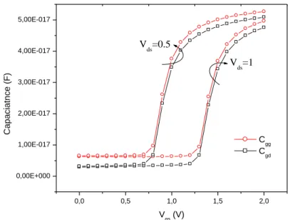
Furthermore, TFET suffers from high gate to drain capacitance that enhances the Miller effect. This enhanced capacitance is principally due to the channel inversion layer while the gate to source capacitance results from the depletion charge [35]. It is worth noting that the majority of the inversion carriers arises from the thermionic emission over the drain built-in potential while the tunneling process has a minor impact on the layer formation [36]. Thus, an increasing of the inversion layer by a lowering of the drain barrier (lower Vds) leads to an
enhancement of the Miller capacitance as depicted in fig 2.7. This effect constitutes a major limitation for ultra-low power applications. Furthermore, the transient analysis of TFET based inverter shows high overshoot/undershoot peaks in the output voltage. In addition, the enhanced capacitance yields higher propagation delay [37]. In consequence, the total power consumption is increased which represents a drawback for low power digital applications. 0,0 0,5 1,0 1,5 2,0 0,00E+000 1,00E-017 2,00E-017 3,00E-017 4,00E-017 5,00E-017 V ds=0.5 Vds=1 C a p a ci a tn ce ( F ) V gs (V) C gg Cgd
26 2.4.3. Transport mechanisms in TFET
If electrons flow from the source to the channel via tunneling process, the transport of the generated carriers over the remaining channel distance to the drain is governed by drift-diffusion transport (DD). Intuitively, TFET can be seen as an ideal gated tunnel diode coupled in series with an ideal MOSFET via an internal node (fig 2.8) [38-39]. Consequently, DD transport can be considered as a limiter of tunneling current.
Figure 2.8 Physical representation of the coupled tunneling and drift-diffusion transport modes.
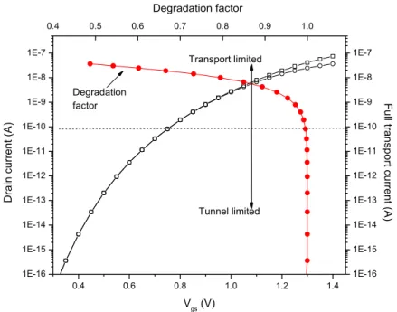
In [39], an interesting demonstration of the effect of coupled transport modes on the tunneling current limitation was performed. For this purpose, the tunneling current was evaluated via the resolution of the Poisson equation with no continuity equation resolving. The current was then calculated by integration of the tunneling generation rate over the volume. It appears that the DD limitation occurs approximately above 10 µA/µm and takes importance with current increasing. Below this limit, the current is tunneling limited which means that all the generated carriers flow through the channel with no limitation. Otherwise, the author proposed another manner of extracting tunneling limited current by setting mobility to infinity and null velocity saturation, we followed this procedure to extract the coupled transport effect in VSG TFET as illustrated in fig 2.9 (the mobility was intentionally decreased in order of 10 cm2/Vs in the full transport mode to amplify the attenuation effect). In this way, it is possible to evaluate the impact of DD transport as an attenuation factor as shown in fig 2.9; the full transport current can then be expressed as
( ) ( , )
ds T T gs ds
![Figure 1.2 Energy versus delay plot of 32bit ALU built from benchmarked devices [7]](https://thumb-eu.123doks.com/thumbv2/123doknet/14896785.651927/10.893.242.644.744.1101/figure-energy-versus-delay-plot-built-benchmarked-devices.webp)
![Figure 2.12 Relation between the off and on-current for InAs based SG, DG, and GAA TFETs for L g =20, 100 nm, T s =5 nm (left panel) and T s =10 nm (right panel) [42]](https://thumb-eu.123doks.com/thumbv2/123doknet/14896785.651927/40.893.113.765.108.373/figure-relation-current-inas-based-tfets-panel-right.webp)
![Figure 2.14 Drain current versus gate voltage for all-silicon DG Tunnel FETs with and without strain profile (L g =50 nm, V ds =1 V) [49]](https://thumb-eu.123doks.com/thumbv2/123doknet/14896785.651927/43.893.217.674.105.385/figure-drain-current-versus-voltage-silicon-tunnel-profile.webp)