Contribution to the study and the design of inverters control « Contribution à l’étude et à la conception des commandes des onduleurs »
118
0
0
Texte intégral
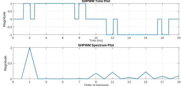
Figure
![Figure 2.2: One phase leg of an inverter with (a) two levels, (b) three levels, and (c) n levels [8].](https://thumb-eu.123doks.com/thumbv2/123doknet/14897505.652181/20.892.199.696.452.688/figure-phase-leg-inverter-levels-b-levels-levels.webp)
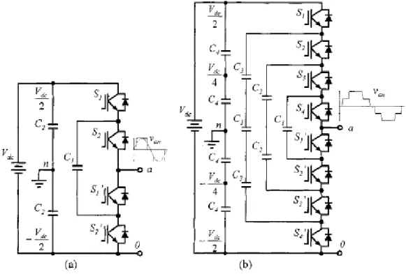
![Figure 2.3: Diode-Clamped Multilevel Inverter Circuit Topologies. a) Three Levels. b) Five- Five-Levels.[8]](https://thumb-eu.123doks.com/thumbv2/123doknet/14897505.652181/22.892.155.750.340.745/figure-clamped-multilevel-inverter-circuit-topologies-levels-levels.webp)
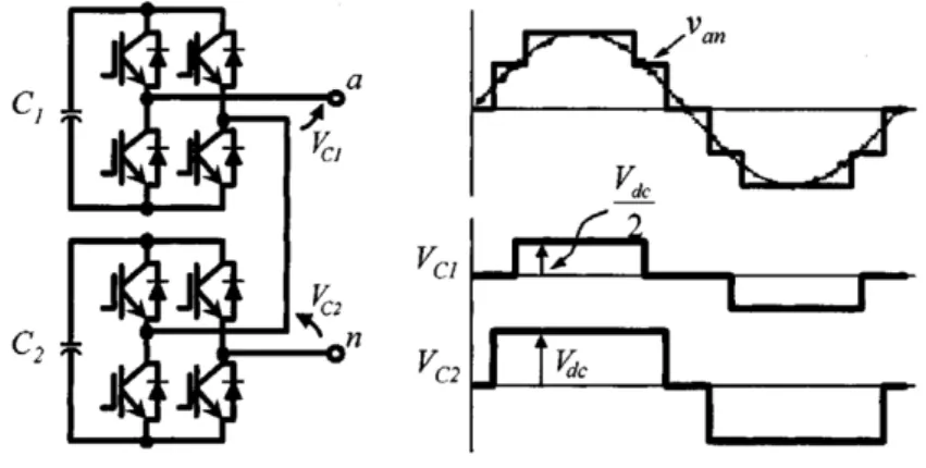
![Figure 2.7: A mixed-level hybrid cell configuration using the thee-level diode-clamped inverter & the cascaded inverter cell to increase the voltage levels [8].](https://thumb-eu.123doks.com/thumbv2/123doknet/14897505.652181/30.892.311.593.470.823/figure-configuration-clamped-inverter-cascaded-inverter-increase-voltage.webp)
+7

![Figure 3.15 shows space vectors for the traditional three, and five-level inverters. [55]](https://thumb-eu.123doks.com/thumbv2/123doknet/14897505.652181/49.892.282.565.199.401/figure-shows-space-vectors-traditional-level-inverters.webp)
Documents relatifs