HAL Id: hal-01407042
https://hal.archives-ouvertes.fr/hal-01407042
Submitted on 1 Dec 2016
HAL is a multi-disciplinary open access
archive for the deposit and dissemination of
sci-entific research documents, whether they are
pub-lished or not. The documents may come from
teaching and research institutions in France or
abroad, or from public or private research centers.
L’archive ouverte pluridisciplinaire HAL, est
destinée au dépôt et à la diffusion de documents
scientifiques de niveau recherche, publiés ou non,
émanant des établissements d’enseignement et de
recherche français ou étrangers, des laboratoires
publics ou privés.
Distributed under a Creative Commons Attribution - NonCommercial - NoDerivatives| 4.0
International License
Nano-proximity direct ion beam writing
Gediminas Seniutinas, Gediminas Gervinskas, Jose Anguita, Davit Hakobyan,
Etienne Brasselet, Saulius Juodkazis
To cite this version:
Gediminas Seniutinas, Gediminas Gervinskas, Jose Anguita, Davit Hakobyan, Etienne Brasselet, et
al.. Nano-proximity direct ion beam writing. Nanofabrication, De Gruyter, 2015, 2 (1), pp.54-62.
�10.1515/nanofab-2015-0006�. �hal-01407042�
the required resolution and footprint of structures these two techniques can be complemented making pattern over-lays [1]. However, both EBL and photolithography have limitations due to several processing steps of resist exposure, etching, metallization required to make a final device. These limitations were overcome with an emergence of focused ion beam lithography (IBL) which enables direct 3D writing. Even though focused ion beam (FIB) milling technology was first demonstrated in the mid-1970s [2,3], it is still mainly used for sample slicing and lamella preparation for transmission electron microscopy. Among several reasons, lack of stable ion sources has hindered FIB applications in high resolution large scale fabrication, especially where He ion sources are implemented. Nonetheless novel ion sources and column geometries providing high temporal beam stability have been developed over the last decade and opened new avenues for the direct writing at the nanoscale. State-of-the-art ion beam lithography tools are capable of patterning relatively large areas with cross sections of 100 × 100 μm2 in tens of minutes [4] depending on complexity and are comparable in speed with mature EBL which is producing 22-nm node lithography masks for the latest microelectronics industry at a throughput ̴5 × 105 μm2 h-1 [5]. High precision direct IBL writing found its way in application fields of photonic crystals [6], single molecule sensors [7], nanopores for DNA probing [8,9] to mention a few. Recent development of new Au, Si, Ge ion sources allows not only milling but also a controlled implantation useful for other nanoscale etching and material growth techniques [10-12].
In plasmonics and nano-photonics, IBL is often used for fabrication/reshaping of nanoscale antennas for the light field confinement and enhancement [13,14] as well as for milling metasurfaces into metal layers [15,16]. Material properties are altered by projectile ion implantation (usually Ga+) around the cuts and this dampens plasmonic or optical resonances of the fabricated structures. With new ion sources Au+, Au2+, Ge+, Si+, Si2+, He+ developed recently and now available commercially, a larger flexibility in material processing at the nanoscale becomes possible. Even though sputtering efficiency of He ions is
DOI 10.1515/nanofab-2015-0006
Received September 2, 2015; accepted November 23, 2015
Abstract: Focused ion beam (FIB) milling with a 10 nm
resolution is used to directly write metallic metasurfaces and micro-optical elements capable to create structured light fields. Surface density of fabricated nano-features, their edge steepness as well as ion implantation extension around the cut line depend on the ion beam intensity profile. The FIB beam intensity cross section was evaluated using atomic force microscopy (AFM) scans of milled line arrays on a thin Pt film. Approximation of two Gaussian intensity distributions describes the actual beam profile composed of central high intensity part and peripheral wings. FIB fabrication reaching aspect ratio of 10 in gold film is demonstrated.
Keywords: Nanofabrication, Ga ion beam milling,
structured light
1 Introduction
Every state-of-the-art nanofabrication technology opens new possibilities in the fast growing field of micro-nano devices. Photolithography and electron beam lithography (EBL) are major fabrication approaches when pattern sizes shrink from micro- to nano-scale. Depending on
Research Article
Open Access
Gediminas Seniutinas*, Gediminas Gervinskas, Jose Anguita, Davit Hakobyan, Etienne
Brasselet, and Saulius Juodkazis
Nano-proximity direct ion beam writing
*Corresponding author: Gediminas Seniutinas, Centre for Micro-Photonics, Faculty of Science, Engineering and Technology, Swinburne University of Technology, Hawthorn, VIC 3122, Australia, & Melbourne Centre for Nanofabrication, 151 Wellington Road, Clayton, VIC 3168, Australia, E-mail: [email protected] Gediminas Gervinskas, Davit Hakobyan, Saulius Juodkazis, Centre for Micro-Photonics, Faculty of Science, Engineering and Techno-logy, Swinburne University of TechnoTechno-logy, Hawthorn, VIC 3122, Australia, & Melbourne Centre for Nanofabrication, 151 Wellington Road, Clayton, VIC 3168, Australia,
Jose Anguita, The Institute of Microelectronics Madrid, Isaac New-ton, 8 PTM, 28760, Spain,
Davit Hakobyan, Etienne Brasselet, University of Bordeaux, CNRS, Laboratoire Ondes et Matière d’Aquitaine, 351 cours de la libération, 33400 Talence, France
Nano-proximity direct ion beam writing 55
very low and current focused He ion beam tools, are more suitable for high resolution imaging rather than large area nanopatterning, a record high resolution ̴3.5 nm and aspect ratio ̴8 ion milling examples were shown with He+ [17,18]. In He FIB systems the ions are pulled by a high tension voltage from a 3-atom-sharp metal tip and have a superb axial directionality. Other ion sources operating by heating filament and pulling desirable ions from a molten atom-thin flow over tungsten tip has a wide distribution in wave vectors of the departing ions, which in addition to a slight variation in thermal energy scrambles their directionality. After passing through ion optical controls in the column, real ion beams have lateral current distribution with peripheral wings which limit the milling resolution of close proximity nanostructures. Since ion beam cuts through different materials at a significantly different rate especially when surfaces are oriented at different angles to the beam [19], presence of the intensity wings is showing up in the fabricated patterns. The decreased patterning resolution in gas assisted etching by ions is even stronger as energy from the beam wings is enough to decompose gas precursor, resulting in faster sidewall material removal [20]. Hence, the beam shape highly affects the achievable resolution, especially in the case of close proximity patterning. These aspects are at the focus of current study and are relevant for fabrication of micro-optical elements endowed with nanoscale features that are sought for the controlled generation of structured light fields, for instance towards precise delivery of optical angular momentum [21].
Different methods to determine the size and shape of the FIB beam, equivalent to the point spread function in optics, were measured by knife edge [22] or mechanical probes placed between the beam and the target [23,24]. However, these methods do not provide accurate measurements due to their low signal-to-noise ratio especially when using low ion beam currents ̴1 pA for high spatial resolution fabrication. Other methods for measuring ion beam profiles are based on ion damage to a substrate [25,26] and require intricate sample preparation procedures as well as sophisticated equipment to evaluate Ga+ lateral distribution in the beam. Theoretical approaches have also been developed to infer the ion beam profile based on mathematical simulation being the ion beam approximated by a Gaussian distribution [22,27]. However, none of these methods answer the following question: what is the real patterning resolution and how close can the nano-features be milled for different aspect ratio nano-patterns?
Here, a simple Pt film milling method is demonstrated for determination of Ga+ intensity cross section where
particular choice of Pt is taken to minimize re-sputtering effects. The method can be implemented easily to check milling response of different materials in actual nanofabrication tasks. High resolution and aspect ratio ion milling capability is eventually illustrated by creating a so-called metallic metasurface whose application potential in optics and photonics has been recently unveiled. This case study highlights the importance of resolution and proximity requirements to be met for future fabrication by FIB.
2 Experimental
To evaluate the lateral distribution of Ga+ in the beam, a 80-nm-thick Pt film was evaporated on a silicon substrate. After milling a test pattern, the samples were inspected by atomic force microscopy (AFM, Nanoscope, Veeco). The AFM cantilever tips (TESP-SS) with curvature radius of 2 nm were used. The high mean free path of the backscattered Pt from the trench minimizes re-deposition, thus offering the possibility to mill with periods smaller than the diameter of the ion beam.
The test pattern consists of ten parallel lines with 10 μm length which allow easy visual tracking when positioning the sample for AFM measurements. Different line arrays have been fabricated, with line periods T ranging from 5 to 100 nm. Every array is milled into the Pt layer using IBL tool (Raith IonLiNE) with the following patterning parameters: energy of Ga+ is 30 keV; electrical current of the ion beam of 1.3 pA; total line dose of 15 nC cm-1, number of loops of 40 that give 0.375 nC cm-1 dose per loop; scanning step of 2 nm and milling depth of 19 nm over a 10 μm × 10 μm write field. FIB milling is carried out at 3.8 × 10⁻⁹ mbar column pressure and high vacuum in the chamber (6.5 × 10⁻⁷ mbar), thus ion scattering by residual gas which influence the beam shape is negligible. The milling is divided into 40 scan loops to minimize differences in etching due to different incidence angles [19] and to reduce re-deposition. If trenches of an array would be etched one by one to their total depth with a period smaller that the ion beam lateral dimensions, the ions that are going to etch a trench just beside already etched one, would hit a surface at an angle larger than 0o to the surface normal. Etching with a number of loops such that all trenches in an array are etched to a depth less than 0.5 nm/loop assures the ions incident angle to be always smaller than 2o at the bottom/top, making negligible the effect of the angle variation in milling. The difference in angle of incidence was also additionally smeared out by various film grain orientations. Finally, we note that
Brought to you by | Université de Bordeaux Authenticated
Vieu et al. has shown that ion beam profile can be well described as a sum of two Gaussian beams representing central core and wings [28]. This is reasonable if we consider that the ion beam is composed of single charged Ga+ ions and their clusters [29].
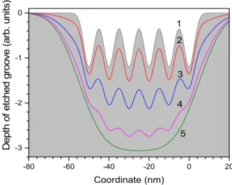
The modeled pattern cross-section using six bi-Gaussian beams is shown in Fig. 1 for illustration. In this example, the two Gaussian distributions composing the beam have diameters of 10 nm and 40 nm for the core and wings, respectively. Influence of the wider beam increases from curve 1 to 5, at which a grating profile at the bottom of the etched grove would disappear. High resolution, closely spaced patterns with nano-scale proximity can only be fabricated then the second Gaussian beam is narrow or at least has much lower intensity than the one describing the beam’s core. The vendor specified full width at half maximum (FWHM) of the beam is 10 nm for the investigated IBL tool. Our used beam waist R at 1/e2 intensity level and FWHM for a Gaussian beam are related:
FWHM =
ln(
4
)
R
R.3.1.2 Exponential ion distribution around the core
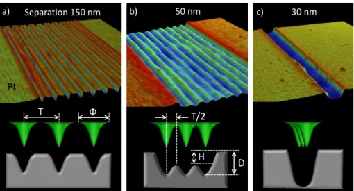
Beam profile estimation by analyzing milled grating profile has been suggested by Anguita et al. [30]. However, the method is able to evaluate only peripheral beam wings and does not give information regarding the core region. Their approach is based on AFM measurements of a crest height in the middle of the milled lines’ array. The necessary parameters used to determine the beam profile are shown in Fig. 2 insets. The lines in Fig. 2b were milled with separation, T, smaller than the beam diameter, φ = 2R. The presence of wings is then observed due to cumulative dose in the overlapped regions. The axial ion beam current distribution is then retrieved according to [30]:
D
H
r
J
T
r
J
2
)
0
(
)
2
/
(
B B=
=
=
(1)where the factor 2 on the right hand side accounts for overlap of two consecutive beam wings that doubles milling dose, with milled depths H and D being defined in Fig. 2b. Note that finite value of H is reminiscent of beam overlap and Eqn. 1 is valid only when condition H < D is fulfilled; otherwise it means that more than two beams overlap. Here we propose to overcome this limitation by analyzing an array as a whole system and to take into account dose contribution, C, for a particular line delivered by milling all the neighboring structures. In our case for the fifth line shown in red in Fig. 3 inset, the total dose contribution to the line can be estimated using the following equation:
Fig. 1. Modeling of the etched array profile milled with two-com-ponent Gaussian beam with diameters φ = 10 nm and 40 nm (e-2
intensity level) mixed at different ratios I10 nm : I40 nm [(1)- 1.2:0.0;
(2)- 1.0:0.2; (3)- 0.6:0.6; (4)- 0.2:1.0 and (5)- 0.0:1.2] for the same
total intensity (ion current). Spacing between the six milled grooves is T = 10 nm. -80 -60 -40 -20 0 20 -3 -2 -1 0 5 4 2 3 D ept h of et ched gr oove ( ar b. uni ts) Coordinate (nm) 1
since the fabrication time of a grating is of the order of a few seconds, both the beam and stage drifts between subsequent milling loops are likely to have negligible influence to the structures.
3 Results and discussion
3.1 Beam profile evaluation
Gaussian components are assumed for the core and wing sections of the ion beam as follows from the mechanism of point source emission of ions from a molten flow of a micro-film.
3.1.1 Gaussian core and wings portions of the ion-beam
It can be assumed that for flat surfaces the etch rate depends only on the local density of ions in the beam J(r), where r is the distance from the beam center. When milling rate and material re-deposition are small (i.e., the lowest currents of 0.2−1.0 pA) the milled groove cross-section maps the local ion beam current density. The ion current density in beam wings is low, so the influence in etching and sputtering is revealed by reducing separation between the milled lines to form regions of overlapped wings and hence accumulated dose. In that case, the effect of the cumulative dose in milling of a material can be investigated by modeling overlaps of bi-Gaussian beams.
Nano-proximity direct ion beam writing 57
profile can be analyzed using generic exponential decays given by J(r) = J(0)e-απr2, which are close to the Gaussian profile discussed above; α is the fitting parameter defining a radial ion current decrease. Fig. 3 shows the fitting of experimental data, where each data point represents evaluated ion current density applying Eqns. 1 and 2. Core region, which extends to 7.5 nm from the beam center, is not included into the fitting since only two data points are available and is only used as the upper bound of the central part. Increasing the radius, a local ion concentration decays following an exponential law (Fig. 3). The first slower decay extends from 7.5 nm to 22.5 nm and probably is associated with distortion of the core region composed
∑
= = =+
+
=
4 1 5 5th1
2
i r iT T rC
C
C
(2)here, the first term takes into account the dose which is delivered by directly milling that line, the second term accounts for the dose that the line receives when the farthest line (displaced by 5T) is being milled, and the third term represents the current dose when the other eight lines at distances from T to 4T are being scanned. This model allows to evaluate the beam profile going for even smaller T values (in our case below 25 nm), where cores of the adjacent beams overlap. The method does not require extended calculations and is suitable for determination of the beam profile and patterning capabilities. The AFM mapped surface profiles for a few periods are shown in Fig. 2. The lines appear separated and the initial surface level between the etched grooves is preserved for T = 150 nm (Fig. 2a). Reducing the period makes beam wings to overlap and areas in between the trenches to accumulate additional dose while milling the neighboring lines (Fig. 2b), and as a consequence the surface level is reduced by H. For the smallest separations the lines completely overlap and single trench with much larger depth is obtained (Fig. 2c). The mapped profiles are analyzed applying Eqns. 1 and 2, which allow estimation of ion concentration at the distance T/2 from the beam center, thus by having a set of different T gratings it is possible to probe ion distribution across the beam. Since the actual beam profile is affected by the ion column optics: stigmatism and deflection plates, the measured
50 nm b) H D 30 nm c) T/2 Ф T Separation 150 nm Pt a)
Fig. 2. Atomic force microscopy (AFM) surface height plots of the ion milled equally separated 10 lines on 80-nm-thick Pt films. Lines are separated by (a) 150, (b) 50, (c) 30 nm. Ion current was 0.5 pA, color scale corresponds to the height span of images from left to right: (-35.2 / +19.2 nm), (-14.1 / +9.7 nm), and (-15.3 / +7.7 nm); insets show overlapping of the beams and parameters used to evaluate the beam profile.
Fig. 3. Fitting of Ga ion beam profile estimated using Eqns. 1 and 2, which was applied for the red line shown in the inset. The core region extends to the radius of around 7.5 nm.
0 500 1000 1500 2000 2500 3000 3500 -4.0 -3.5 -3.0 -2.5 -2.0 -1.5 -1.0 -0.5 0.0 0.5 1.15e-0.00073r2 4.15e-0.00152r2 Core region (r = 7.5 nm) Experimental data ln(J(r)/J(0)) r(nm)]2 T
Brought to you by | Université de Bordeaux Authenticated
of single charged Ga+ ions having narrow energy distribution. The second function represents a distorted Gaussian beam which is formed by ion clusters which have larger energy variation. Even though the extended beam wings are much weaker as compared to the core, but their presence reduces patterning resolution, especially in the case of the close proximity milling.
3.1.3 Direct fitting of the AFM profiles
The method discussed above is based on building up the beam profile by evaluating a crest height in different period gratings. Another possible approach to estimate lateral ion distribution in the beam is direct fitting of the entire grating profile. The ion distribution is well fitted by a bi-Gaussian function:
(3)
where I1,2 and R1,2 are the fitting parameters representing the amplitude and half width of the beam at e-2 intensity level, respectively. The AFM tip shape causes a false surface profile when surface roughness becomes smaller than the probe dimensions. To restore original surface profile deconvolution with the tip shape should be applied, which is a lengthy and complicated procedure. To avoid that, the fitting is done for gratings with the period smaller than 65 nm, where the gratings are flat enough for accurate AFM mapping. Fig. 4b shows the profile of the used probe compared to the measured grating roughness.
The best fit curves obtained by applying Eqn. 3 for the arrays with line spacing of 55 nm and 45 nm are shown in Fig. 4a and b, respectively. The crest in between the lines is lower than the initial surface due to the overlapped beam wings which sputter material. The tendency is clear for the smaller periods where the overlap reaches even higher ion beam intensity part. Sets of fitting parameters for the arrays with periods 45 to 60 nm are shown in Fig. 4c and d. The beam waist for the core is 3 times narrower as compared to the wings region. However, the
Fig. 4. Digitized plots of AFM height profile fitted with two Gaussian components: a) T = 55 nm and b) T = 45 nm. Variation of the best fit parameters for different grating periods: c) beam waist, d) normalized weighting coefficients: (I1,2/(I1 + I2)) · 100%.
100 125 150 175 200 225 0 5 10 15 20 25 Grating fit (R1 = 9.54 nm; R2 = 34.76 nm) Experimental data Z ( nm ) X coordinate (nm) 45 50 55 60 5 10 15 20 25 30 35 R (nm) Period (nm) R1 R2 45 50 55 60 20 40 60 80 100 I1 I2 Coeficient weight (%) Period (nm)
a)
c)
b)
d)
100 125 150 175 200 225 0 5 10 15 20 25 Grating fit (R1 = 7.70 nm; R2 = 32.58 nm) Experimental data Z (nm) X coordinate (nm)Nano-proximity direct ion beam writing 59
ion beam profile inscribed into the Pt film by milling. The effect of faster milling at larger incident angle, 50° and 83°, for the ions in beam’s wings is accounted in the profiles (3) and (4), respectively. For comparison, the beam profile estimated applying method discussed in previous section as well as vendor provided profile are presented in the same graph as curves (1) and (5), respectively. The curve (5) has been obtained according to the measurement method reported earlier [20]. It is based on ion implantation but not sputtering and reveals spatial extent of substrate amorphisation in area irradiated by the focused ion beam. The method provides a lateral ion distribution profile, however, it requires intricate procedures and cannot be directly used for process development in the ion milling tasks. Nonetheless, the vendor specified beam profile and the one evaluated by analyzing close proximity line arrays are comparable and both reveal the beam waist to be around 10 nm at FWHM.
In practice, having narrow ion beam not necessarily guarantees high patterning resolution. Properties of material being milled play significant role as well, especially when fabricating high aspect ratio structures where re-deposition becomes an issue. Platinum used method shows that the wider part of the beam has a
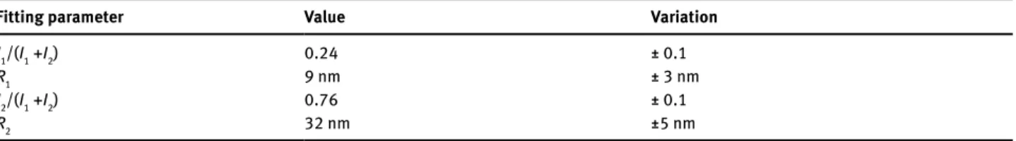
stronger contribution to a groove formation. For clarity the normalized values of intensity parameters are summarised in Fig. 4d. Noteworthy, the proposed method is based on measurement of the milled surface profile as compared to the knife edge techniques or material amorphisation analysis. This involves possible redeposition and angular milling effects, but eventually it shows the actual nanopatterning capability and quantifies proximity effects when milling at high resolution. The evaluated beam parameters are summarized in Table 1.
According to the fitting data, the second Gaussian term representing wings contributes to the milling almost three times more than the central part. This implies that the most of ions are distributed in the wings, if one assumes milling is proportional to the ion number density. However, the main contribution of the tails is due to the sputtering rate dependence on ions’ incidence angle [19]. Larger angles give higher sputtering yield; hence the material in the tail regions is removed faster.
It is well known that material milling rate strongly depends on the angle between projectile ion and normal to the surface [31,32]. Sidewalls of the milled trenches always have a slanted profile, thus it requires less ions to remove the same amount of material than in the beam center where ions hit the surface vertically. The slope angle in the wings region was evaluated to be around 50° for the milled arrays. For our investigated Ga ions accelerated at 30 kV and Pt as a target material, the milling rate at normal incidence angle is almost 2.1 times slower than at 50°. Moreover, ions in the wing regions have wave vectors which are not parallel to the beam’s optical axis and hit material at even higher angles. The fastest material removal in our experimental configuration is at 83° and it is around 11 times higher as compared to normal incidence. This means ions hitting the surface at around 83° are removing the material 11 times faster [33]. The faster milling in peripheral regions can be accounted by scaling down the amplitude of the wider Gaussian component, which in this case should be 11 times smaller than initially obtained from the fitting.
Beam profile extracted by fitting the milled line arrays is shown in Fig. 5 as (2). This line represents Eqn. 3 with the averaged fitting parameters from Table 1 and describes the
Table 1. Beam parameters obtained via fitting of the surface profile of the milled line array.
Fitting parameter Value Variation
I1/(I1 +I2) 0.24 ± 0.1
R1 9 nm ± 3 nm
I2/(I1 +I2) 0.76 ± 0.1
R2 32 nm ±5 nm
Fig. 5. Comparison between Ga ion beam profiles evaluated using different methods: (1) by using Eqns. 1 and 2; (2) by Eqn. 3 without accounting for faster milling by the wings; (3) same as (2) but normalised for the wing contribution at 50o; (4) same as (3) just
normalized for 83o angle; and (5) the vendor provided beam profile
obtained by the method described in [20] (courtesy Raith GmbH).
(2), (3) and (4) are plotted for the averaged fitting parameters from
different grating periods, T.
0 5 10 15 20 25 30 35 40 45 50 0.0 0.2 0.4 0.6 0.8 1.0 1 2 3 4 5 J(r)/J(0) r (nm)
Brought to you by | Université de Bordeaux Authenticated
promising for cuts through thick metal layers with nano-precision. This is very appealing for photonics community that demonstrates a growing interest in planar optical elements endowed with subwavelength features – so called metasurfaces [38,39]. Metasurfaces are sought for topological shaping of light, especially at small scale and many applications of arbitrary shaped slits to control and reshape light field have already been reported [40,21,41]. Although planar optical elements are very attractive for their small footprint and ability to be integrated on various photonic chips, the used metal films are usually thin (< 100 nm) and do not completely block the background light. This might be a drawback in envisioned applications as the beam which was reshaped by metasurface further interacts with the background. As a demonstration of focused ion beam milling enabled high efficiency optical elements, we designed and fabricated a metallic metasurface in a 200 nm-thick Au layer, see Fig. 7, that enables the generation of optical vortices from an incoming circularly polarized light via so-called spin-orbit interaction. The performance of such metasurfaces [42,43] strongly depends on the fill factor of the pattern and, hence, requires the highest fabrication precision. Present was intentionally selected for our experiments as its
re-deposition is minimal and the beam profile evaluation is more precise. However, for the most of practical applications gold is a material of choice. Re-sputtering of gold and grain pattern makes additional challenge for high resolution nanopatterning of metasurfaces, which are gaining an increasing interest in photonics community.
3.2 Highest resolution and aspect ratio ion
milling
FIB and its IBL implementation are relatively new nanofabrication techniques proving useful for an increasing number of applications [11,34]. Resist exposure, ion beam induced deposition [35] and selective masking [36] are methods realized by IBL patterning. IBL also offers a direct write capability which is very attractive for fast prototyping and 3D structuring. Featuring a few hundred of nanometers depth of focus, the technique allows greyscale fabrication on complex 3D structures without losing the resolution.
Fabrication of high aspect ratio and close proximity nanogrooves is the most challenging task of modern nanotechnology which should develop methods of nanofabrication superior to the current CMOS 22-nm-resolution masks. High resolution EBL followed by etching steps is a common approach, however the aspect ratio at nanoscale resolution is ̴3−4 [37] as etching gasses cannot effectively diffuse into narrow slits. To test IBL capabilities of milling high aspect ratio slits using previously estimated beam shape, a single line has been milled through 220 nm thick gold layer on a glass substrate and then the substrate was halved to reveal the cross-section of the cut. Fig. 6 shows the obtained scanning electron microscopy (SEM) image of a ̴20 nm width cut and reveals the high aspect ratio of ̴10 achieved for a soft material such as gold.
The demonstrated high aspect ratio milling is
Fig. 6. SEM image of a 45-degree-tilted 20 nm groove milled in 220 nm Au film on a glass substrate. The substrate was halved to reveal the side view of the cross-section.
100 nm 100 nm
Glass
Gold
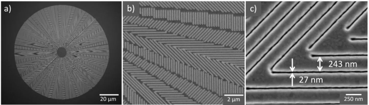
̴20 nm 220 nmFig. 7. SEM images of a) 100 μm diameter optical element, the q-plate inscribed in 200 nm thick gold layer using focused Ga ion beam. b) and c) the close up views of the fabricated patterns. Width of the cut is around 27 nm with a period of parallel lines of 270 nm.
a)
b)
c)
20 µm 2 µm 250 nm
243 nm
27 nm
Nano-proximity direct ion beam writing 61
example consists of azimuthally varying nanogratings made of slits having a width of around 30 nm cut over a 100 μm diameter area. The fabricated pattern was consistent all over the structure showing the high temporal beam stability and precise stage positioning. The device has shown superb performance across the entire visible wavelengths range giving high optical vortex purity [44].
4 Conclusions
Close proximity milling has been demonstrated making different period gratings. When the period gets comparable or smaller than the focused ion beam diameter, the initial surface erosion occurs due to cumulative ion dose from the beam wings. The proposed AFM profiling method can be used as a simple practical tool to estimate ion beam profile and to evaluate the resolution limits for the given material, ion beam tool, and the beam conditions (current, aperture, acceleration voltage). AFM height profile of milled arrays is well fitted with two Gaussian components representing core and wing regions of the beam. Full width at half maximum of ~10 and ~40 nm have been found for the central and outer beam parts, respectively, and is comparable with the vendor specified value which has been evaluated using a complex amorphisation analysis. High resolution patterning of 20 nm grooves of aspect ratio of 10 is demonstrated in a gold film. Focused ion beam patterning of complex metallic metasurface where close spacing of grooves is required reveals state-of-the-art capabilities of the technology.
Acknowledgment: JA acknowledges funding support
from the Spanish MICINN with the grant “Salvador de Madariaga”. SJ is grateful for partial support via the Australian Research Council DP130101205 Discovery project. EB and DH thanks the financial support from the French State, managed by the French National Research Agency (ANR) in the frame of the ’Investments for the future’ Programme IdEx Bordeaux – LAPHIA (ANR-10-IDEX-03-02). Authors are grateful to Drs. Achim Nadzeyka and Sven Bauerdick for discussions on technical implementation aspects of IBL and ion sources. This work was performed in part at the Melbourne Centre for Nanofabrication (MCN) in the Victorian Node of the Australian National Fabrication Facility (ANFF).
References
[1] G. Seniutinas, G. Gervinskas, E. Constable, A. Krotkus, G. Molis, G. Valušis, R. A. Lewis, and S. Juodkazis. Thz photomixer with milled nanoelectrodes on LT-GaAs. Applied Physics A, 117(2):439–444, 2014.
[2] R. Levi-Setti. Proton scanning microscopy: feasibility and promise. Scanning Electron Microscopy, 125, 1974. [3] W. H. Escovitz, T. R. Fox, and R. Levi-Setti. Scanning
transmission ion microscope with a field ion source. Proceedings of the National Academy of Sciences, 72(5):1826–1828, 1975.
[4] G. Seniutinas, G. Gervinskas, A. Balcytis, F. Clark, Y. Nishijima, A. Krotkus, G. Molis, G. Valušis, and S. Juodkazis. Nanoscale precision in ion milling for optical and terahertz antennas. In SPIE OPTO, pages 93740P–93740P. International Society for Optics and Photonics, 2015.
[5] C. Marrian and D. M. Tennant. Nanofabrication. Journal of Vacuum Science & Technology A, 21(5):S207–S215, 2003. [6] S. Juodkazis, L. Rosa, S. Bauerdick, L. Peto, R. El-Ganainy,
and S. John. Sculpturing of photonic crystals by ion beam lithography: towards complete photonic bandgap at visible wavelengths. Optics Express, 19(7):5802–5810, 2011. [7] J. Li, D. Stein, C. McMullan, D. Branton, M. J. Aziz, and J. A.
Golovchenko. Ion-beam sculpting at nanometre length scales. Nature, 412(6843):166–169, 2001.
[8] J.Li, M. Gershow, D. Stein, E. Brandin, and J. A. Golovchenko. DNA molecules and configurations in a solid-state nanopore microscope. Nature Materials, 2(9):611–615, 2003.
[9] A. Kotnala and R. Gordon. Double nanohole optical tweezers visualize protein P53 suppressing unzipping of single DNA-hairpins. Biomedical Optics Express, 5(6):1886, 2014. [10] S. Bauerdick, L. Bruchhaus, P. Mazarov, A. Nadzeyka, R.
Jede, J. Fridmann, J. E. Sanabia, B. Gila, and B. R Appleton. Multispecies focused ion beam lithography system and its applications. Journal of Vacuum Science & Technology B, 31(6):06F404, 2013.
[11] C. Chang and A. Sakdinawat. Ultra-high aspect ratio high-resolution nanofabrication for hard x-ray diffractive optics. Nature Communications, 5, 4243, 2014.
[12] S. Tongay, M. Lemaitre, J. Fridmann, A. F. Hebard, B. P. Gila, and B.R. Appleton. Drawing graphene nanoribbons on sic by ion implantation. Applied Physics Letters, 100(7):073501, 2012. [13] E. J. R. Vesseur, R. De Waele, H. J. Lezec, H. A. Atwater, F.J.
Garcia De Abajo, and A. Polman. Surface plasmon polariton modes in a single-crystal au nanoresonator fabricated using focused-ion-beam milling. Applied Physics Letters, 92(8):083110, 2008.
[14] G. Gervinskas, G. Seniutinas, L. Rosa, and S. Juodkazis. Arrays of arbitrarily shaped nanoparticles: Overlay-errorless direct ion write. Advanced Optical Materials, 1(6):456–459, 2013. [15] U. Levy, H. C. Kim, C. H. Tsai, and Y. Fainman. Near-infrared
demonstration of computer-generated holograms implemented by using subwavelength gratings with space-variant
orientation. Optics Letters, 30(16):2089–2091, 2005. [16] J. Lin, J. P. B. Mueller, Q. Wang, G. Yuan, N. Antoniou, X.
C. Yuan, and F. Capasso. Polarization-controlled tunable directional coupling of surface plasmon polaritons. Science, 340(6130):331–334, 2013.
Brought to you by | Université de Bordeaux Authenticated
[17] O. Scholder, K. Jefimovs, I. Shorubalko, C. Hafner, U. Sennhauser, and G. L. Bona. Helium focused ion beam fabricated plasmonic antennas with sub-5 nm gaps. Nanotechnology, 24(39):395301, 2013.
[18] A. I. Kuznetsov, A. E. Miroshnichenko, Y. H. Fu, V. Viswanathan, M. Rahmani, V. Valuckas, Z. Y. Pan, Y. Kivshar, D. S. Pickard, and B. Luk’yanchuk. Split-ball resonator as a three-dimensional analogue of planar split-rings. Nature Communications, 5, 3104, 2014.
[19] Q. Wei, K. D. Li, J. Lian, and L. Wang. Angular dependence of sputtering yield of amorphous and polycrystalline materials. Journal of Physics D: Applied Physics, 41(17):172002, 2008. [20] S. Tan, R. Livengood, Y. Greenzweig, Y. Drezner, and D. Shima.
Probe current distribution characterization technique for focused ion beam. Journal of Vacuum Science & Technology B, 30(6):06F606, 2012.
[21] E. Brasselet, G. Gervinskas, G. Seniutinas, and S. Juodkazis. Topological shaping of light by closed-path nanoslits. Physical Review Letters, 111(19):193901, 2013.
[22] J. Orloff, J. Z. Li, and M. Sato. Experimental study of a focused ion beam probe size and comparison with theory. Journal of Vacuum Science & Technology B, 9(5):2609–2612, 1991. [23] J. G. Lopes, J. Rocha, L. M. Redondo, and F. C. Alegria. High
resolution ion beam profile measurement system. Proceedings of ICALEPCS2011, Grenoble, France, 2012.
[24] C. E. Sosolik, A. C. Lavery, E. B. Dahl, and B. H. Cooper. A technique for accurate measurements of ion beam current density using a faraday cup. Review of Scientific Instruments, 71(9):3326–3330, 2000.
[25] J.B. Wang and Y.L. Wang. A novel procedure for measuring the absolute current density profile of a focused gallium-ion beam. Applied Physics Letters, 69(18):2764–2766, 1996.
[26] C. M. Park, J. A. Bain, T. W. Clinton, P. A. A. Van der Heijden, and T. J. Klemmer. Measurement of Ga implantation profiles in the sidewall and bottom of focused-ion-beam etched structures. Applied Physics Letters, 84(17):3331–3333, 2004.
[27] D. Petit, C. C. Faulkner, S. Johnstone, D. Wood, and R. P. Cowburn. Nanometer scale patterning using focused ion beam milling. Review of Scientific Instruments, 76(2):026105, 2005. [28] C. Vieu, G. B. Assayag, and J. Gierak. Observation and
simulation of focused ion beam induced damage. Nuclear Instruments and Methods in Physics Research Section B: Beam Interactions with Materials and Atoms, 93(4):439–446, 1994. [29] R. G. Forbes. Understanding how the liquid-metal ion source
works. Vacuum, 48 (1):85–97, 1997.
[30] J. Anguita, R. Alvaro, and F. Espinosa. A new experimental method to obtain the ion beam profile of focused ion beam nanotechnology systems. IJMEM, 1:61, 2012.
[31] Y. Yamamura, Y. Itikawa, and N. Itoh. Angular dependence of sputtering yields of monatomic solids. Institute of Plasms Physics IPPJ-AM-26, Nagoya University, 1, 1983.
[32] Y. Yamamura and H. Tawara. Energy dependence of ion-induced sputtering yields from monatomic solids at normal incidence. Atomic Data and Nuclear Data Tables, 62(2):149–253, 1996.
[33] Focused ion beam sputtering yield calculator. http://www. asu.edu/clas/csss/NUE/FIBSputterCalcYamamura.html, 2015 Jul.
[34] X. Wang, S. Xie, J. Liu, S. O. Kucheyev, and Y. M. Wang. Focused-ion-beam assisted growth, patterning, and
narrowing the size distributions of ZnO nanowires for variable optical properties and enhanced nonmechanical energy conversion. Chemistry of Materials, 25(14):2819–2827, 2013. [35] M. Esposito, V. Tasco, F. Todisco, A. Benedetti, D. Sanvitto,
and A. Passaseo. Three dimensional chiral metamaterial nanospirals in the visible range by vertically compensated focused ion beam induced-deposition. Advanced Optical Materials, 2(2):154–161, 2014.
[36] W. McKenzie, J. Pethica, and G. Cross. A direct-write, resistless hard mask for rapid nanoscale patterning of diamond. Diamond and Related Materials, 20(5):707–710, 2011.
[37] G. Seniutinas, L. Rosa, G. Gervinskas, E. Brasselet, and S. Juodkazis. 3D nano-structures for laser nano-manipulation. Beilstein Journal of Nanotechnology, 4(1):534–541, 2013. [38] N. Yu, P. Genevet, M. A. Kats, F. Aieta, J. P. Tetienne, F.
Capasso, and Z. Gaburro. Light propagation with phase discontinuities: generalized laws of reflection and refraction. Science, 334(6054):333–337, 2011.
[39] D. Lin, P. Fan, E. Hasman, and M. L. Brongersma. Dielectric gradient metasurface optical elements. Science,
345(6194):298–302, 2014.
[40] A. Nadzeyka, L. Peto, S. Bauerdick, M. Mayer, K. Keskinbora, C. Grévent, M. Weigand, M. Hirscher, and G. Schütz. Ion beam lithography for direct patterning of high accuracy large area x-ray elements in gold on membranes. Microelectronic Engineering, 98:198–201, 2012.
[41] C. F. Chen, C. T. Ku, Y. H. Tai, P. K. Wei, H. N. Lin, and C. B. Huang. Creating optical near-field orbital angular momentum in a gold metasurface. Nano Letters, 15(4):2746–2750, 2015. [42] E. Karimi, S. A .Schulz, I. De Leon, H. Qassim, J. Upham, and R. W. Boyd. Generating optical orbital angular momentum at visible wavelengths using a plasmonic metasurface. Light: Science & Applications, 3(5):e167, 2014.
[43] G. Zheng, H. Mühlenbernd, M. Kenney, G. Li, T. Zentgraf, and S. Zhang. Metasurface holograms reaching 80% efficiency. Nature Nanotechnology, 10(4):308–312, 2015.
[44] D. Hakobyan, H. Magallanes, G. Seniutinas, S. Juodkazis, and E. Brasselet. Tailoring orbital angular momentum of light in the visible domain with metallic metasurfaces. Advanced Optical Materials, DOI: 10.1002/adom.201500494, 2015.