Developing Cuprous Oxide Thin Film Characterization Techniques to Illuminate Efficiency-Limiting Mechanisms in Photovoltaic Applications
by
Riley Eric Brandt Submitted to the
Department of Mechanical Engineering
in Partial Fulfillment of the Requirements for the Degree of Bachelor of Science
at the
Massachusetts Institute of Technology June 2011
© 2011 Riley Brandt All rights reserved
The author hereby grants to MIT permission to reproduce and to
distribute publicly paper and electronic copies of this thesis document in whole or in part in any medium now known or hereafter created.
Signature of Author……… Department of Mechanical Engineering May 16, 2011 Certified by………
Tonio Buonassisi SMA Assistant Professor of Mechanical Engineering and Manufacturing Thesis Supervisor Accepted by………...
John H. Lienhard V Collins Professor of Mechanical Engineering Chairman, Undergraduate Thesis Committee
Developing Cuprous Oxide Thin Film Characterization Techniques to Illuminate Efficiency-Limiting Mechanisms in Photovoltaic Applications
by
Riley Eric Brandt
Submitted to the Department of Mechanical Engineering
on May 16, 2011, in partial fulfillment of the requirements for the degree of Bachelor of Science in Mechanical Engineering
Abstract
Future fossil fuel scarcity and environmental degradation have demonstrated the need for renewable, low-carbon sources of energy to power an increasingly industrialized world. Solar energy, with its extraordinary resource base, is one of the most feasible long-term options for satisfying energy demand with minimal environmental impact. However, solar photovoltaic panels remain expensive and employ materials whose resource bases cannot satisfy global, terawatt-level penetration. This necessitates the development of cheap, earth-abundant semiconductors for solar conversion such as cuprous oxide (Cu2O). Poor solar energy conversion efficiency (<2%) has hindered the development of this material, yet it is not well understood what is preventing the material from approaching the idealized maximum efficiency of 20%. The present work aims to develop a thorough characterization method for Cu2O thin films fabricated through a physical vapor deposition (PVD) process known as reactive direct-current magnetron sputtering. This both provides a platform for material analysis and an opportunity to adapt a typically high-throughput manufacturing method to make high quality thin films. Spectrophotometry, Hall Effect mobility measurement, and photoelectrochemical cell techniques are used in succession to determine the absorption and transport properties. The films are found to have a direct forbidden bandgap of 1.93 eV, with an absorption coefficient of greater than 105 cm-1 for photons carrying energy in excess of 2.6 eV. Majority carrier mobility is measured as 58.1 cm2/V⋅s, approaching the levels of monocrystalline oxidized films in literature. These high mobilities indicate that with carrier lifetime >10 nanoseconds, minority carrier diffusion length could easily exceed the film thickness. The photoelectrochemical minority carrier diffusion length measurement achieves success on gallium arsenide test samples, determining flat-band potential, quantum efficiency, and minority carrier diffusion length, paving the way for future Cu2O measurement. Future work may apply this test procedure to fully characterize other materials, and eventually lead to solar cell fabrication.
Thesis Supervisor: Tonio Buonassisi
Acknowledgments
As a high school student deeply interested in applying technology to the major global issues of our time, the Massachusetts Institute of Technology was a natural choice. Yet at one point, the goal of attending and furthermore graduating from MIT seemed very far off. Between the reality now and that distant past lie a number of individuals that have made this journey possible.
Firstly, I must thank the incredible generosity of MIT and its community for providing me the opportunity to pursue my passions here. In particular I must thank the donors of the Audrey Stein Memorial and Class of 2001 Student Life Scholarship Funds, whose contributions provided me the means to achieve at MIT. Furthermore, I owe a great deal to the generosity of the Undergraduate Research Opportunities Program (UROP), whose funding enabled me to conduct the research that eventually led to the creation of this thesis.
Secondly, I wish to thank the many academic advisors that have provided me the tools to succeed in the sometimes overwhelming arena that is MIT. Most notably, I thank Professor John Brisson for his advice as an academic advisor, and Professor Carol Livermore for trusting me and for allowing me to prove to myself that I could handle academic research in my first ever UROP.
Thirdly, I wish to express a tremendous amount of gratitude to the individuals who directly advised me on my work with the Laboratory for Photovoltaics. Graduate students Yun Lee and Sin Cheng Siah provided both their extensive wisdom and extra pairs of hands to conduct experiments and achieve results. Most importantly though was the role of my advisor, Professor Tonio Buonassisi. Professor Buonassisi introduced me to the science of photovoltaics, then entertained my first research proposal and provided me the individuals and resources to pursue it. Since then, his optimism, wisdom, and oversight have consistently driven my work on this project.
Finally, and most importantly, I must thank my parents for their trust and support in the last four years and beyond. They were willing to accept a 17-year-old’s dream of traveling hundreds of miles to start a new life at MIT, and ever since have provided endless motivation and reassurance. For getting me here, and helping me not only survive but thrive, I will never be able to thank them enough.
Contents
1 Introduction 12
1.1 Motivation . . . . 12
1.2 Problem Statement . . . . 15
1.3 Aims and Objectives . . . . 17
2 Physics 17
2.1 Photovoltaic Cell Basics . . . 17
2.2 Optical Absorption . . . . 18
2.3 Mobility and Diffusivity . . . 26
2.4 Recombination and Carrier Diffusion Length . . . 30
3 Experimental Techniques 33
3.1 Sample Preparation . . . . 33
3.2 Spectrophotometry . . . . 38
3.3 Hall Effect Mobility . . . . 41
3.4 Photoelectrochemical Cell for Diffusion Length . . . 45
4 Results and Analysis 50
4.1 Test Sample . . . . 50
4.2 Absorption Measurement . . . . 52
4.3 Mobility Measurement . . . 54
4.4 Photoelectrochemical Cell Measurement . . . 56
5 Conclusions and Next Steps 57
List of Figures
1-1 Available solar resource
1-2 Solar competitiveness vs. the grid
1-3 Quantity of material required to supply world's electricity with solar power 1-4 Shockley-Queisser solar cell efficiency limit
2-1 The electromagnetic spectrum
2-2 AM0, AM1, and AM1.5 solar spectrums
2-3 Energy bands forming at small interatomic spacing 2-4 Photoexcitation of valence band electrons
2-5 Direct and indirect band transitions 2-6 Random diffusion of different gas species
2-7 Photocurrent composition in a metal-semiconductor interface 3-1 Comparison of thin film deposition techniques
3-2 Physical vapor deposition experimental configuration
3-3 Crystal grain sizes for different substrate deposition temperatures 3-4 Deposition process parameters
3-5 Gold contact locations
3-6 Perkin Elmer Lambda 950 Spectrophotometer 3-7 Spectrophotometer diagram
3-8 Reflective spectrophotometer measurement 3-9 Transmissive spectrophotometer measurement 3-10 Fabry-Perot interferometer ray tracing
3-11 Hall Effect diagrams
3-12 Hall Effect contact positions 3-13 Hall effect sample holder and setup 3-14 Contact resistance plot
3-15 Photoelectrochemical cell schematic 3-16 Photoelectrochemical cell
3-17 Band bending at p-type semiconductor-electrolyte interface 3-18 Band bending of PEC junction under different biases
3-19 I-V curve of PEC junction
4-1 GaAs current vs. wavelength plots 4-2 I-V curves for GaAs
4-3 Reflectance and transmittance of Cu2O film
4-4 Absorption coefficient of Cu2O as a function of photon energy 4-5 Forbidden direct bandgap absorption fit
List of Tables
1.1 EIA energy cost estimates in 2016
Nomenclature Constants
c = 2.998 x 10⁸ m⋅s-1 Speed of light in free space h = 6.626 x 10⁻³⁴ J⋅s Planck Constant
kB = 1.381 x 10⁻²³ J⋅K-1 Boltzmann Constant mo = 9.109 x 10⁻³¹ kg Free electron mass q = 1.602 x 10⁻¹⁹ C Elementary charge Variables
α Absorption coefficient [cm-1] C Capacitance [F]
D Diffusivity [cm2⋅s-1]
E Energy [J], Electric Field Strength [V⋅cm-1] Φ Photon flux [s-1]
G Generation rate [cm-3⋅s-1] I Intensity [W⋅cm-2] J Current density [A⋅cm-2] k Wave vector [m-1] L Diffusion length [cm] λ Wavelength [nm] m Mass [kg] m* Effective mass [kg] µ Mobility [cm2⋅V-1⋅s-1] N Number of states [1]
n Index of Refraction [1], Concentration of electrons [cm-3] ν Frequency [s-1]
P Probability [1]
p Concentration of holes [cm-3] QF Internal Quantum Efficiency [1] R Resistance [Ω]
ρ Resistivity [Ω⋅cm] σ Conductivity [Ω-1⋅cm-1] T Temperature [K] t Film thickness [nm]
τ Relaxation time, carrier lifetime [s] V Voltage [V]
W Width [cm] x Distance [cm]
1. Introduction 1.1 Motivation
In 2010, civilization consumed over 500 exajoules of energy and in the process emitted over 30 billion metric tons of carbon dioxide [1]. It is difficult to comprehend such numbers – this energy consumption would be the equivalent of running 300 billion 50-watt light bulbs simultaneously for an entire year. As staggering as these numbers are, they are projected to grow. Annual global energy consumption may surpass 1000 exajoules in the next century given current trends [1]. As the inhabitants of non-OECD countries climb out of poverty and demand the lifestyles enjoyed by those in the developed world, resource consumption will grow accordingly. For individuals, this trend of higher energy consumption will enable upward mobility and, as it has done in the developed world, will make consumers wealthier and healthier with every additional unit of energy consumed.
To the collective, however, this disturbing trend represents the primary challenge of the 21st century. In a classic tragedy of the commons scenario, such massive resource consumption threatens civilization. By 2100 we may have exhausted our fossil fuel reserves, displaced hundreds of millions of people with rising sea levels, and spoiled our climate with desertification, pollution, and acidified oceans. Humanity’s perpetual desire for increased prosperity and its means of attaining it are coming to a head, and thus the 21st century will require major changes to ensure long-term sustainability of civilization.
The change necessary to prevent catastrophic climate change is, quite simply, to reduce anthropogenic CO2 emissions. A simplistic model describing net CO2 emissions can be summarized in the following equation:
! CO2 = Population " Energy Population " CO2 Energy. (1) This identity breaks down the problem of CO2 emissions into its underlying causes – growing population, increasing standard of living (energy per capita), and the carbon intensity of energy usage. Analyzing each term individually, it is clear the first two are difficult targets for addressing carbon dioxide emissions. The population problem has no technical or rapid solution, and as energy per capita is closely tied to prosperity, we expect this to rise inevitably with the growing affluence of the undeveloped world. We can, however, directly address the amount of CO2 emitted per unit of energy consumed through technological innovation. This will require a transition to lower carbon sources of energy, consisting primarily of nuclear, geothermal, hydro, wind, and solar power.
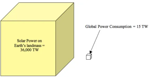
Of all of these alternatives, solar represents perhaps the most promising long-term option. Whereas nuclear relies on an exhaustible fuel source with its own issues of waste production, and geothermal and hydro can only be deployed in a limited number of geographical areas, sun and wind power are accessible over much of the globe. Of the latter two technologies, solar offers a much larger resource base to capture. In fact, given an average solar flux of 1366 W/m2, over 600 exajoules of solar energy (more than we currently consume in a year) strikes the earth’s surface every hour. It is for these reasons that the author believes that solar energy is the necessary long-term solution to the energy and climate crises.
Figure 1-1: Available solar energy resource base compared to the current global energy demand.
However, the generation of useful energy from the sun’s radiation still presents two critical challenges. Firstly, the cost of solar energy is still prohibitively expensive in most markets. Grid electricity sells for around 10-20 cents/kw⋅hr; and the cheapest sources such as coal can produce below this price. Table 1.1 provides an Energy Information Administration (EIA) comparison of the cost of current technologies, with fossil fuels in the 9-14 ¢/kw⋅hr range and photovoltaics just over 30 ¢/kw⋅hr [2].
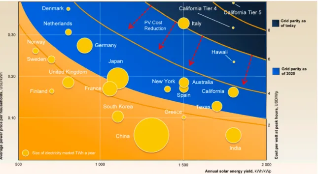
To attain a competitive levelized cost of electricity over the lifetime of the plant, a commonly accepted metric is that the solar panels must cost below $1 per peak watt produced. In other words, a 1 m2 panel rated at 100 W under a peak solar spectrum (1000W/m2 of intensity) must cost no more than $100 to purchase and install for it to compete with grid electricity rates over its lifetime. This is the holy grail of photovoltaic research known as “grid parity” – where the levelized cost of producing electricity from the sun drops below market electricity rates and therefore becomes economically viable without subsidies. Fig. 1-2 demonstrates how close current technologies are to achieving this in sunny climates with higher market electricity rates.
Figure 1-2: From McKinsey report on solar competitiveness, comparing the dollar-per-peak-watt price of solar panels with potential locations for installation, based on local electricity prices and the availability of the solar resource. The horizontal axis compares the annual solar yield, the left axis indicates retail electricity rates, and the curved lines at right indicate grid parity at different installed prices in $/Wp [3].
With the least expensive plants installing solar panels for $6/Wp, solar is already surpassing grid parity in markets with high solar yield and high grid electricity rates. It will take a significant reduction in cost, however, to reach global grid parity and penetrate the larger electricity markets in the US, China, and much of the industrializing world.
The second barrier to widespread photovoltaic deployment is the availability of materials. Currently, photovoltaic modules make up a very small percentage of the world’s energy base, at less than 0.1% [2]. To produce hundreds of exajoules of electricity, solar panels will need to be manufactured at the scale of more ubiquitous products such as automobiles or plastic bottles. At this scale, the materials involved in production become a major limiting factor. Materials such as tellurium, gallium, or indium used in modern solar cells are rare, and will never scale to cover the many square miles necessary to power the world with solar. Even ignoring the obvious problem of insufficient supply, using a scarce material presents a crippling economic paradox.
Proponents of solar energy expect solar cells to achieve increasing returns to scale, such that the cost of producing cells drops as processes are refined and high-throughput factories are built. Yet, the economics of scarce resources suggest that as demand for a material increases and supply remains fixed, the price will grow prohibitively instead.
There are two important steps that the photovoltaic industry can take in addressing the material constraint, and in turn the cost constraint. The first is to move towards thin film solar cells, requiring significantly less absorber material than industry standard silicon-based cells. The second is to use earth abundant materials in place of the more rare semiconductors that are researched today. There has been increasing attention placed on this field of earth abundant thin-film solar cells recently, as solar advocates realize the need to plan for terawatt-level capacity in the future [4].
Surveying all of the possible semiconductors available for solar applications, it is possible to classify them by the quantity of material reserves and the cost of the material to predict which would be the most scalable candidates, as seen in Fig. 1-3.
Figure 1-3: Estimated material requirements for 22 semiconductors to achieve worldwide electricity output as compared to available production and reserves of these materials, emphasizing importance of relative abundance [4]
One of the most promising options is cuprous oxide (Cu2O), a group II-VI semiconductor with a cubic lattice arrangement of oxygen and monovalent copper atoms. Oxygen is the most abundant element on earth, and copper, while not as common in the earth’s crust, claims an extensive mining operation that already produces over 16 million tons of copper annually [5]. The promise of cuprous oxide is therefore its low cost and high availability. If a Cu2O solar cell could reach grid parity in mass production, it could rapidly scale to satisfy humanity’s 1000 exajoule energy demand all over the globe. 1.2 Problem Statement
The promise of Cu2O as a photovoltaic material has not gone unnoticed. The earliest publication suggesting the viability of a Cu2O solar cell dates from 1960 [6]. In
the years since this publication, silicon has become the dominant solar cell material, while no successful Cu2O cell has ever been produced. This is due in large part to the poor performance of existing devices – the maximum published efficiency of a solar cell fabricated from Cu2O is 2.0% [7]. This figure is far from the potential performance of an ideal Cu2O cell.
A commonly used metric for evaluating the maximum potential of a solar cell is the Shockley-Queisser efficiency limit [8]. This calculation compares the energy of incoming solar photons with the minimum photon energy required to generate current in a solar cell, also known as the bandgap of the semiconductor. If the bandgap is too high, lower energy photons cannot be absorbed at all, and go to waste. On the other hand, if the bandgap is too low, higher energy photons will only donate a small fraction of their energy to generating electricity. We can therefore predict what the maximum efficiency of a solar cell would be given the spread of photon energies the sun emits. Fig. 1-4 displays the maximum efficiency expected at each bandgap based on this spectrum.
Figure 1-4: The predicted maximum efficiency of a single-junction solar cell in AM0 sunlight, as a function of the bandgap of the semiconductor [8].
Cuprous oxide is known to have a bandgap of roughly 2.0 electron volts (eV), which corresponds to a maximum theoretical efficiency of 20%. Silicon solar cells with a maximum theoretical efficiency of 32% have reached over 25% in practice, proving that it is possible to approach the maximum, ideal efficiency with improvements in material quality and cell architecture. This is a promising sign for cuprous oxide, as it suggests that such a cell could achieve efficiencies much higher than the current best-published 2% figure.
This raises the question, what is limiting Cu2O cell efficiency? Fundamentally, what is preventing the consistent conversion of incoming photons to usable electricity?
In general, problems can arise in the generation, transport, and separation of electric carriers in a cell. With respect to carrier generation, a semiconductor could be a poor absorber. Crystalline silicon, for example, with an indirect bandgap, requires a semiconducting layer two orders of magnitude greater than thin film materials (e.g.
cadmium telluride) because of its poor absorption. However, Cu2O is a direct bandgap semiconductor with strong absorption (an absorption coefficient of over 105 cm-1 for >2.6eV energy photons in the present work), suggesting that given proper antireflective cell design, a Cu2O thin film cell would have no problem generating carriers.
With respect to carrier separation, this is primarily an issue of proper junction and module engineering. Cu2O, however, does exhibit a very high exciton binding energy of approximately 150 meV [9]. This means that for incoming photons with energy just above the bandgap, electrons and holes may not be distinctly formed and will instead form an exciton pair that is much more difficult to separate.
This leaves carrier transport, the most likely candidate affecting Cu2O performance. One can summarize the properties of how rapidly carriers like electrons diffuse through a semiconductor and how often they recombine, or relax down to a non-useful energy state before being extracted, with one metric – the minority carrier diffusion length. This describes the average length that we may expect a minority carrier (e.g. an electron in a p-type semiconductor) to travel before recombining with a carrier of opposite charge. To extract the carriers generated by incoming radiation, they must have a diffusion length on the order of the thickness of the device. If the diffusion length is too short, many of the carriers will recombine or go to waste before being extracted and used in an external circuit.
1.3 Aims and Objectives
In light of the above discussion, it is clear how critical it is to better understand the semiconducting properties of Cu2O. As the most likely reason for poor efficiency is poor transport properties, it is particularly important to look at the transport properties of the Cu2O thin films produced in our lab.
Thus, the aim of the present work is to build upon two important research efforts in the Laboratory for Photovoltaics at MIT. Firstly, we have developed an improved physical vapor deposition method using high-temperature annealing to deposit high quality p-type Cu2O films; and secondly, we have begun characterizing these films to compare to existing literature. The purpose of the present work is to review and develop a procedure for measuring absorption, majority carrier mobility, and minority carrier diffusion length of thin film semiconductors. It is hoped that formulating these techniques will lay the groundwork for fully understanding Cu2O. This understanding will both help determine what exactly is limiting cell efficiency, and provide a clear direction for how material improvements might help solve the problem of poor performance.
2. Physics
2.1 Photovoltaic Cell Basics
Photovoltaic (PV) cells are devices that convert the electromagnetic energy carried by light into electrical energy. First conceived in 1839 by Alexandre-Edmond Becquerel, it would take over a century before scientists could engineer the materials necessary to build a highly efficient solar cell. This section seeks to describe the basic principles of a solar cell, and the effect of certain material properties on the cell’s performance.
The sun, formed at the birth of the solar system 4.6 billion years ago, is the primary source of energy for life on this planet. Inside the dense center of the sun, gravitational force and high temperatures force hydrogen molecules to undergo fusion, forming higher mass elements and releasing tremendous amounts of nuclear energy in the process. This positive feedback loop helps drive the sun’s temperature higher and instigate further fusion reactions, resulting in temperatures of 13.6 million Kelvin (K) in the core and approximately 5800 K at the surface. As the molecules that make up the sun’s mass reach such high temperatures, they vibrate with a tremendous amount of kinetic energy and emit this energy in the form of electromagnetic radiation. This radiation travels in all directions, illuminating earth and donating its energy to the life contained here. The primary mechanism for this energy conversion is photosynthesis, where plant matter absorbs particles of light energy, called photons, to do work and drive chemical reactions within the plant.
Solar cells, an inorganic corollary to photosynthesis, allow for the conversion of the sun’s electromagnetic energy into usable electricity. Incoming photons excite electrons in the cell’s absorbing material, a semiconductor, giving them enough energy to conduct. These excited electrons leave behind a hole, a positively charged “particle” akin to a bubble of air in water. The electrons and holes diffuse separately through the material until they reach a junction, usually formed at the interface of two different semiconducting materials. The electric field at the junction causes the negatively charged electron to move in one direction and the positively charged hole to move in the other direction, and the only way they may recombine is by traveling through an external circuit. A free, conducting electron traveling through a circuit is the basis for electricity. Thus, by generating free carriers (electrons and holes) and extracting them out of the cell, they may do useful work in the same way that a battery would supply such free carriers to power a light bulb, motor, or any other electrical device.
This general picture of how a solar cell converts electromagnetic energy (photons) into electrical energy (electrons and holes) gives us a simple model for understanding the performance of a solar cell. This performance depends on three primary steps - the ability to generate free electrons and holes from photons, the ability of those photogenerated carriers to travel through the cell, and finally, the ability to separate and extract those carriers from the cell. In improving the performance at each step, one can create a highly efficient solar panel that produces the maximum possible electricity. The following sections will discuss in more detail how each physical process works, thereby illuminating the potential limiting factors.
2.2 Optical Absorption
Understanding how photons interact with a solid semiconducting material is a critical part of understanding how photovoltaic cells work. To understand absorption, however, one must first understand the atomic structure of a semiconductor and the physics of light.
2.2.1 Electromagnetic Radiation
As Bohr first postulated in 1913, atoms consist of a dense, positively charged nucleus surrounded by a cloud of negatively charged electrons. These electrons, according to Bohr’s quantum mechanics, can only exist in very specific “quantized”
energy levels, or orbits. Each orbit corresponds to a certain amount of energy, and thus to move between orbit levels the electron must absorb or release energy. The most common form of energy transfer is the photon – a quantum particle or wave containing electromagnetic energy equivalent to the frequency at which the wave vibrates, ν, multiplied by the Planck Constant, h = 6.626 x 10⁻³⁴ J⋅s such that
!
Ephoton = h" . (2) Photons may be modeled as either a particle or a wave, and both interpretations are of use in the current work. As a wave, light can be characterized by its temporal frequency ν and spatial wavelength λ. In free space, the relationship between how often the wave oscillates and how far it travels in one oscillation determines the speed of light,
!
c = "# . (3)
Thus, photons of light, while always traveling at the same speed, may oscillate at any frequency and carry any amount of energy. Electromagnetic radiation is therefore naturally represented by a spectrum, as illustrated in Fig. 2-1. Photons oscillating at high frequencies contain higher energy (kilo-electron volts) but shorter wavelengths (picometers), while lower frequency photons contain much smaller energies (milli-electron volts) and longer wavelengths (kilometers). Between these two extremes lies the visible region, at wavelengths from 380-740nm. Human eyes have evolved to perceive this small subsection of the electromagnetic spectrum because the sun emits most intensely in this region. By evolutionary coincidence, the part of the spectrum that we perceive through sight is also the most relevant region for producing electricity from the sun.
Figure 2-1: The EM spectrum, with visible wavelengths from 380-740nm [10].
The region of the electromagnetic spectrum over which the sun emits is defined by a property known as blackbody radiation. A blackbody is a substance with 100% emissivity and absorptivity – in other words, all incident photons are fully absorbed. Over the visible spectrum, such a material would appear jet black as no incident light is scattered backwards, giving rise to the name “blackbody”. At the surface of the sun, lightweight hydrogen molecules vibrate with high kinetic energy, as the surface temperature averages 5800 K. The acceleration of electric charge creates a sinusoidal time-varying electric field, in turn generating a time-varying magnetic field, and it is this coupled field that forms a photon.
However, what we perceive as temperature is in reality an average of kinetic energy over many molecules. While 5800K corresponds with a kinetic energy of 0.5 electron volts (eV), the atoms at the surface of the sun contain a wide spread of kinetic energies. In turn, the atoms vibrate and emit over a wide range of frequencies. The range of frequencies emitted can be characterized by Planck’s Law, expressed here as the emitted power per unit area, per unit solid angle, per unit frequency:
! I(") =2h" 3 c2 1 e h" kBT #1 $ % & & ' ( ) ) . (4)
Alternatively, Planck’s Law may be expressed as a function of wavelength:
! I(") =2hc 2 "5 1 e hc "kBT #1 $ % & & ' ( ) ) . (5)
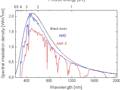
Given the sun’s surface temperature of 5800 K and the solid angle tended by the Earth, the solar spectrum may be determined from this equation, as seen in Fig. 2-2.
Figure 2-2: The solar spectrum displaying energy flux at each wavelength. The graph displays the difference between the ideal spectrum and what is actually observed as a result of attenuation. [11]
As seen in Fig. 2-2, the actual spectrum observed at the earth’s surface differs from the ideal blackbody spectrum predicted, for two reasons. Firstly, the surface of the sun is not an ideal blackbody emitter as the temperature can vary substantially, radiation is absorbed and re-emitted, and sporadic flares allow for significant variation in emissions. Furthermore, the 100 kilometers of atmosphere through which incoming radiation must travel tends to absorb a fraction of the electromagnetic energy. Water vapor and ozone in particular cause scattering across a wide number of wavelengths, most noticeably reducing the intensity of higher energy ultraviolet (below 380nm wavelength) radiation. Some molecules like CO2 and water vapor are also strongly absorptive over specific bands of the spectrum, corresponding to natural resonant frequencies for these molecules.
To capture the affect of the atmosphere on solar radiation (“insolation”) intensity, we can characterize the flux on a solar panel by the amount of atmosphere it must travel through. Air-mass 0, or AM0 insolation describes the solar spectrum before entering the atmosphere, as a satellite orbiting Earth might encounter. Air-mass 1, or AM1, describes the distance the insolation must travel through the atmosphere directly perpendicular to the earth’s surface, or the minimum distance possible. The most commonly used spectrum is the AM1.5, which represents an atmosphere thickness 1.5 times the minimum, or what a panel might receive from the sun at a 48.2° angle from normal. As the sun’s angle (and therefore atmospheric distance it must travel through) varies according to time of day and latitude, the AM1.5 spectrum is a common standard.
In summary, the sun emits a broad spectrum of photons of many different wavelengths and energies. This spectrum is determined by the temperature distribution at the surface of the sun, and has a peak intensity at 520 nm or 2.4 eV. This solar spectrum strikes the earth with a power flux of 1366 W/m2 before entering the atmosphere. The atmosphere then attenuates the intensity by absorbing or scattering some photons, resulting in a modified spectrum striking a solar panel at ground level. These photons are then absorbed by the solar panel to produce useful electricity.
2.2.2 Semiconductor Band Structure
Bohr’s atomic model describing quantized, specific energy levels for each electron is effective only for single atoms. It does not explain the structure of atoms when assembled in a solid. As trillions of atoms are forced together in a crystal lattice, their interatomic spacing becomes so small that the electron clouds of neighboring atoms begin to overlap. In metals, the electrons effectively become a single cloud throughout the material, and can move around freely between atoms. This phenomenon gives rise to a metal’s high conductivity.
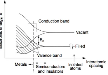
Semiconductors, as their name suggests, form a more complicated electronic structure. As the atoms get closer, the many electron levels in the individual atoms merge to form two specific energy bands. Fig. 2-3 demonstrates how many s, p, d, or f electron orbitals can join to form two distinct energy levels – a valence and conduction band.
Figure 2-3: Small interatomic spacing leads the individual orbital levels to split and form different electron energy structure as seen here. At a certain interatomic distance those levels can be defined as two energy bands [12].
The lower energy grouping is referred to as the valence band (where electrons are less mobile), while the higher energy band is referred to as the conduction band (where electrons are free to move throughout the solid). In a pure semiconductor, no electrons can inhabit the energy levels in between these two bands. This forbidden region is known as the bandgap. It is important to recognize that the valence and conduction levels do not represent single energy levels for electrons and holes, but rather represent the boundaries of acceptable electron and hole energy states.
At temperatures of 0 K, all electrons inhabit the valence band in a semiconductor, reducing conductivity to zero. However, as the temperature rises, electrons in the valence band can achieve high enough thermal energy to be thermally excited into the conduction band. The temperatures need not be substantial – at room temperature, where the average kinetic energy is 26 meV, a small fraction of electrons obtain enough energy to jump bandgaps two orders of magnitude greater. As the temperature rises further, more electrons can move into the conduction band (leaving holes behind in the valence band), which enables higher conductivity in the semiconductor.
2.2.3 Absorption
Solar cell operation, however, relies on a more direct form of energy transfer between valence and conduction bands: the photogeneration of carriers. As discussed previously, each photon carries with it a specific amount of energy. If a photon’s energy exceeds the difference in energy between the valence and conduction bands, the photon can be absorbed by an electron in the valence band and will be promoted into the conduction band. Fig. 2-4 demonstrates this phenomenon of photo-excitation pictorially. Note that the larger the bandgap, the less likely it is that carriers can move into the conduction band. These materials form a familiar class known as insulators, incapable of electrical conductivity due to the lack of charge carriers populating the conduction band.
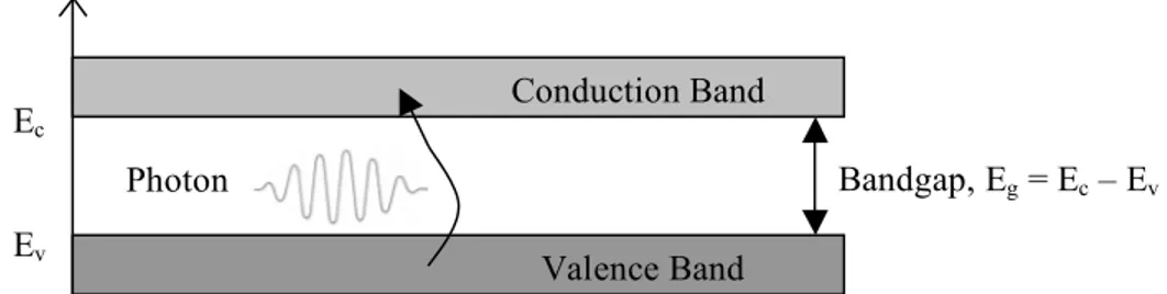
Figure 2-4: A valence band electron absorbing a photon’s energy and being excited into the conduction band, if Ephoton > Eg.
Photons with energy in excess of the bandgap are readily absorbed, as they are likely to have enough energy to excite electrons that are not right up against the band edge. However, for photons just above the bandgap, the thermal spread of carriers away from the band edges may prevent carrier excitation. Thus, we expect absorption to grow exponentially as a function of photon energy above the bandgap. This absorption strength is quantified with the absorption coefficient α [cm-1]. The intensity I(x) of incoming radiation in watts is attenuated in the material according to this absorption coefficient and the distance traveled such that
I(x) = IOe "#x. (6) Conduction Band Valence Band Bandgap, Eg = Ec – Ev Photon Ec Ev
Lower energy photons, with a lower probability of absorption, must on average travel a further distance through the material before being absorbed; hence they would have a smaller absorption coefficient.
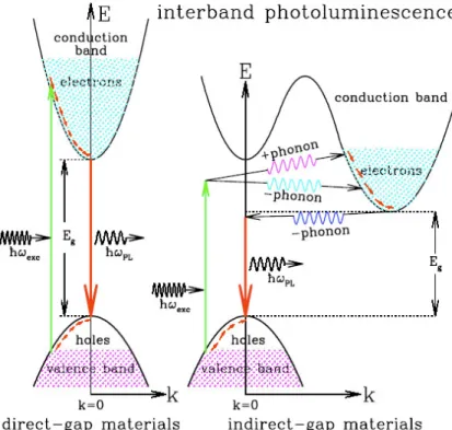
The absorption coefficient provides a highly effective way of characterizing the likelihood of free charge carriers to be excited into the conduction band, as a function of the incoming photon energy. This coefficient, however, varies substantially depending on whether the cell has a direct or indirect bandgap. A direct bandgap indicates that the minimum distance between valence and conduction energy bands occurs at a single momentum. Thus, the electron may absorb the photon and directly jump into the conduction band with no change in momentum. However, in an indirect bandgap semiconductor, the valence band energy peak and conduction band energy minimum occur at two different momentums. Thus, the electrons must undergo a change in momentum in addition to photon absorption in order to be fully excited into the conduction band. Fig. 2-5 displays this difference pictorially.
Figure 2-5: Direct vs. indirect bandgaps, with momentum on the abscissa and energy on the ordinate. Both require the same energy transfer for a carrier to move between bands, however in the indirect case, an additional momentum transfer must occur [13].
J. Bardeen, F. J. Blatt, and L. H. Hall have derived an extensive model to describe how the absorption coefficient may vary as a function of photon energy for different energy band transitions [14]. Their theory pertains specifically to absorption near the band edge, or for photons with energies on the order of the bandgap of the semiconductor. We assume first that photons carry a negligible amount of momentum such that momentum transfer only occurs through phonons, or lattice vibrations. Furthermore, we assume that the absorption coefficient for a particular energy of photon is proportional to the probability of transition from initial to final state Pif, proportional to
the densities of electrons in initial state, ni, and proportional to the density of empty final states, nf. Summing this up over all possible transitions of energy equal to hv:
!
"(h#) = A
$
Pijninf. (7)For the purposes of these derivations, we make the additional assumption that the semiconductor is undoped and at 0 K, specifically entailing that all valence states are filled and all conduction band states are initially empty.
For direct band-to-band transitions, no momentum transfer occurs; there is a single transition for which the probability is independent of momentum. Each initial energy level Ei on the valence band maps directly to a final energy level Ef on the conduction band, related by the photon energy such that
!
Ef = h" # Ei. (8)
The bands are approximated as parabolic as in Fig. 2-5, thus if we take Ev to indicate the maximum energy of the valence band and Ec to be the minimum energy of the conduction band, we can describe the energy-momentum relationship for the valence and conduction bands respectively as:
! Ev " Ei = h2 k2 2me# , (9) ! Ef " Ec = h2 k2 2mh# . (10)
Here, ħ = h/2π, k is momentum (wave vector), and me* and mh* are the effective masses of the electrons and holes respectively. This produces a relationship between the wave vector and the energy a photon must have in excess of the bandgap (Eg):
! h" # Eg = h2k2 2 1 me$ + 1 mh$ % & ' ( ) * . (11)
The three dimensional density of states for fermions like electrons and holes can be defined as ! N(h")d(h") =8#k 2 dk (2#)3 , (12)
which describes the number of states available at each wave vector k. Combining equations (11) and (12), we obtain an expression for the absorption coefficient as a function of photon energy:
! "(h#) = q2 2 me $ + 2 mh $ % & ' ( ) * 3 2 nch2me $ (h# + EG) 1 2 ,"(h#) - (h# + EG) 1 2 . (13)
In summary, the absorption coefficient for direct transitions at the band edge is, to first order, proportional to the energy in excess of the bandgap, to the 1/2 power. This relationship is very useful for modeling basic direct transitions and for determining the bandgap of a material from its absorptive properties, but it only describes direct band-to-band transitions.
In addition, it is possible to have forbidden direct transitions as a result of quantum selection rules [14]. Here, transitions at k=0 are forbidden, and the transition
probability scales with k2 elsewhere. For these transitions, due to the additional k2 factor, the absorption coefficient is instead:
!
"(h#) $ (h# % EG)
3
2. (14)
Indirect transitions are more difficult to model, as they require an additional momentum transfer in the form of a phonon. This phonon must contain a certain momentum corresponding to the difference in band edges, and additionally contains energy Eph. As a phonon may be emitted or absorbed during the transition, there are two possible energy transitions that may occur:
{
!
h" = Ef # Ei+ Eph h" = Ef # Ei# Eph
. (15)
Additionally, the density of initial and final energy states can be modeled as in the direct case as, respectively
! N(Ei) = 1 2"2h2(2mh #)32(E v $ Ei) 1 2 (16) ! N(Ef) = 1 2"2h2(2me #)32(E f $ EG) 1 2. (17)
As in the direct case, the absorption coefficient is proportional to the product of the final and initial densities of states, described in (16) and (17), integrated over all states separated by the energy difference hv±Eph. It is also proportional to the probability of interacting with a phonon, a function of the number of phonons:
! Nph = 1 exp Eph kBT " # $ % & ' (1 . (18)
After integrating the products of densities of states and multiplying by the probability of phonon interaction, the absorption coefficients may be calculated as
! "+(hv) = A(hv # EG+ Eph) 2 exp Eph kBT $ % & ' ( ) #1 , (19) ! "#(hv) = A(hv # EG # Eph) 2 exp Eph kBT $ % & ' ( ) #1 , (20) ! "(hv) ="+(hv) +"#(hv), (21)
where α+ describes absorbing a phonon and α- describes emitting a phonon, and the sum of the two represents the net absorption coefficient.
The individual equations are not of critical importance to the present work, as a semiconductor may display several different types of band transitions, resulting in more complicated behavior than simple models would suggest. However, the general form is helpful for making sense of experimental data. In all three models discussed above. The absorption coefficient is of the form
"(h#) = A(h# $ EG)
m . (22)
In other words, α is always proportional to the difference between photon energy and the bandgap, to some exponent m. For direct allowed transitions, m = 1/2, for direct
forbidden transitions m = 3/2, and for indirect allowed transitions m = 2. Fitting experimental data to this model thus not only reveals the band gap but also the type of transition that is occurring.
2.2.4 Carrier Generation
Finally, the attenuation equation (6) provides a platform for calculating the generation rate of carriers at any point in the device. Assuming that each time a photon is absorbed, an electron and hole are generated, we can derive an equation for the generation of carriers G as a function of depth in the material, given an incoming photon flux of Φ. For each wavelength,
!
G ="#e$"x. (23)
This equation will become useful later on in determining the photocurrent output of the device, which is highly dependent on the number of carriers generated.
In conclusion, photons of a wide variety of energies are incident on a solar cell. We typically approximate this range of photon energies as the AM1.5 spectrum, incorporating mostly photons in the visible spectrum. Photons with insufficient energy to create a pair of separate charge carriers are not absorbed, while photons with energy in excess of the bandgap are absorbed. Their absorption probability is affected by whether the transition is direct, forbidden, or indirect. Using this energy-dependent absorption coefficient, we can describe the frequency with which new conducting electrons are created, which is critical for determining the electrical output of our solar cell. Thus, we can fully model how incoming light leads to electricity in a Cu2O thin film solar cell. Experimental methods in the present work will evaluate whether Cu2O displays a direct or indirect transition at the band edge, and thus allow us to determine its absorption characteristics and bandgap. This fully explains the first stage of solar electricity generation and provides the groundwork for understanding solar cell performance.
2.3 Mobility and Diffusivity
Once electrons and holes are generated, they must diffuse towards a junction to be separated, and then to a pair of positive and negative contacts in order to be extracted. A junction effectively provides an electromotive force to separate electrons and holes, and then acts a potential barrier such that once the separated electrons and holes cross the junction, they remain apart.
Eventually, as the carriers diffuse through a solid, the negatively charged electrons will recombine with a positively charged hole. Ideally, this recombination will occur outside of the device, where the charge carriers can do useful work. If the electron and hole recombine inside the photovoltaic cell, that energy they absorbed may go to waste. Thus, understanding how quickly electrons and holes move through the semiconductor is an important precursor to understanding how well a solar cell performs.
Conduction band electrons and valence band holes can move freely throughout the semiconductor, while their oppositely charged counterparts are fixed to their host atom. These carriers tend to move through the material with an average velocity determined by their thermal energy. They move in one direction until colliding with an atom or particle in the solid’s crystal lattice, and then scatter in another random direction. This describes, for the most part, the typical motion of free carriers in an unbiased semiconductor. The net displacement of each carrier is zero, as all motion is random.
However, under two different forces, drift and diffusion, carrier motion can become more coherent.
The first of these patterns, diffusion, is not so much an active force but rather a consequence of the random motion of carriers. When the concentration of carriers in one volume is greater than the concentration of carriers in a neighboring volume, on average, more carriers will move into the lower concentration half than the higher concentration half. This phenomenon of diffusion is easily understood in an analogy with gas mixing. Two neighboring compartments of distinct gases are shut off from one another. Gas molecules on each side move randomly in all directions. When the barrier is removed, gases from each side begin to randomly venture into the opposite side. As long as there is still a greater concentration of one gas in the right half, there will always statistically be more movement of that gas from right to left than vice versa. The system of two gases displays a natural tendency towards equilibrium. To get there, it displays what are described as diffusion currents.
Figure 2-6: Different gas molecules, or electrons and holes, randomly mixing through randomized thermal motion [16].
Electrons and holes behave in much the same way as two distinct gases. In areas with a higher concentration of electrons than elsewhere, we will see a net flow of more electrons out than in. We can describe these differences in concentration of carriers as gradients. For one-dimensional flow, we can model the diffusion current as directly proportional to the concentration gradient of either negative or positive charge carriers [15] such that ! Jdiff ,n = +qDn dn(x) dx , (24) ! Jdiff , p = "qDp dp(x) dx . (25)
Here, J represents the diffusion current, n(x) and p(x) are the volumetric densities of electrons and holes respectively, and q is the charge of a single carrier. The coefficients Dn and Dp are the diffusivity of electrons and holes respectively, with units of [cm2/s]. This diffusivity is closely related to the conductivity of the material, which will become apparent shortly.
The second mode of carrier motion is drift current. This is the more direct effect of carriers experiencing a force under an external electric field. In addition to random thermal velocity, carriers experience acceleration in the direction of the field for positive charges, or opposite the field for negative charges. This drift current depends on the number of each carrier and the mobility of the carriers.
Mobility is a fundamentally important material property that describes how readily a carrier moves through a material under an electric field. It is measured with the SI units [cm2/V⋅s], indicating that it is a measure of how rapidly carriers diffuse through a cross sectional area under the influence of a potential difference. If one imagines electrons drifting at random through a lattice, they will collide with a lattice atom every time interval τ, which represents the mean time between such scattering events. After each scattering event, their average velocity is randomized, or reset to zero. Therefore the net velocity is affected by the length of time between collisions, and how much force the electric field can exert on the charge – higher charge and lower mass entities are accelerated more strongly. From this random walk theory of conductivity, we can model the mobility of charge carriers in a material as
!
µx = q" mx
#, (26)
where mx* is the effective mass of species x (either holes or electrons). The effective masses of holes and electrons can be very different, resulting in different mobilities for different charge carriers.
Mobility is a particularly useful measure in semiconductors, because it is a more specific depiction of carrier impedance than conductivity. Conductivity, a measure of charge carriers flowing through a conductor per unit time, captures both the mobility of carriers as well as the number of carriers. While not as relevant to the study of metals, these two separate phenomena are uniquely important for understanding semiconductor performance. For electrons, for example, the conductivity can be expressed as
!
"= qnµn. (27)
Considering the one-dimensional conductivity of both electrons and holes in a semiconductor, we produce an expression relating drift current and electric field E,
!
Jdrift = q("nµn+ pµp)E . (28) The competing phenomena of drift and diffusion are what drive the movement of carriers in a solar cell. At the center of each cell is a junction where, typically, two different semiconductors meet. These two materials are at different electrical potentials, and thus the junction region contains a strong electric field formed by the difference in electric potentials across the opposite sides. As carriers are formed all through the device, they tend to diffuse at random. Yet, these carriers are only useful if the negative and positive electron and hole currents can be separated, in order to form a coherent net current flow in one direction. This is where the junction plays a critical role. In the strong, unidirectional electric field at the junction, electrons and holes are forced to move in separate directions. Thus, excess electrons populate one side of the junction while the other side becomes populated similarly by excess holes. For these carriers to recombine, they now must diffuse out through another conductive path into an external circuit, doing useful work in the process.
Outside of the electric field in the junction region, carrier motion is dominated by diffusion. Thus, it is important to understand how readily carriers diffuse. In fact, the
diffusivity discussed earlier is directly related to the carrier mobility, however here the driving force does not come from an electrical potential but rather thermal energy. Relating thermal energy to kinetic energy allows us to formulate what are known as the Einstein relations [15]. These relate diffusivity and mobility as follows:
! Dn = kBT q µn Dp = kBT q µp . (29)
Mobility, and in turn diffusivity, are critically important to good solar cell performance, as we will see in the ensuing sections. Thus, measuring and understanding mobility provides a strong basis for evaluating the performance of a solar cell.
Mobility may be limited by a number of factors, which involve the phenomenon of scattering. By the definition in (26), mobility is directly proportional to the mean time interval between scattering events. Thus, the more frequently scattering events occur, the slower the carrier will move through the material and the lower its mobility will be.
The first type of scattering is phonon scattering [16]. As the temperature of the crystal lattice increases, thermal energy manifests itself in lattice vibrations where the spring-like bonds between atoms transmit acoustic waves. These waves, called acoustic phonons, can collide with electrons and holes and scatter them. The density, heat capacity, and temperature of the material affect the concentration of phonons and therefore the frequency of these scattering events.
The second variety is ionized impurity scattering [16]. A semiconductor lattice typically contains dopants, which are atoms of different valence states that introduce more electrons or holes into the semiconductor. In Cu2O, these could typically be excess oxygen atoms that introduce additional positive charges, or other intended or inadvertent impurities such as nitrogen or iron. This introduction of donor or acceptor atoms is what changes a material’s potential and therefore enables the formation of junctions, however these impurities can be problematic as well. Ionized atoms in a lattice introduce a positive or negative charge, which by Coulomb’s Law can exert a force on electrons or holes. Thus the more dopants or “ionized impurities” present in the lattice, the more frequently their fields will scatter carriers and the smaller the mean scattering time will be.
While phonon and ionized impurity scattering are the dominant mobility-limiting mechanisms, there can also be smaller effects including lattice or surface defects. The cumulative effect of all of these limiting mechanisms can be summarized with Matthiessen’s Rule [16], ! 1 µtotal = 1 µphonon + 1 µimpurities ... . (30)
Matthiessen’s Rule suggests that the mobility solely due to phonon scattering or defects can be combined to give the net mobility. In future sections, we will discuss how to measure mobility, opening the door to understanding the dominant mobility limiting mechanisms. By characterizing the mobility of Cu2O and what limits it, we can better engineer the material to achieve more mobile carriers.
2.4 Recombination and Carrier Diffusion Length
Unfortunately, once free carriers have been created, there is a finite amount of time before they recombine. Electrons in the conduction band and holes in the valence band will recombine if given an impetus to do so. This could occur in a collision with a lattice atom, particularly at a defect site, or in a collision with a phonon or another charge carrier. Thus, it is equally important for carriers to have both a high mobility and a long lifetime to ensure that they reach a point of extraction before recombining.
Typically, three dominant sources of recombination act within a semiconductor – Shockley-Read-Hall (SRH) processes, Auger processes, or simple radiative recombination [16].
SRH recombination typically occurs in highly doped or impure materials, because it relies on the existence of many defect states. In an SRH process, an electron becomes trapped in an energy state just below the conduction band edge (or a hole just above the valence band edge) by an atom in the crystal lattice that introduces this “defect” energy level. Before the carrier has a chance to thermally escape back into its respective band, it recombines with another hole or electron that moves up or down into the same defect energy level.
An Auger recombination event involves three carriers. Here, an electron and hole recombine, but rather than release this energy as a photon or phonon, the energy is transferred into another electron in the conduction band. This electron then slowly loses this extra energy as heat as it relaxes back down to the conduction band edge. This form of recombination scales proportionally to the carrier concentration.
Finally, the simplest form of recombination is direct, radiative recombination. Here, the exact opposite of photogeneration occurs – a conduction band electron and valence band hole recombine and release a photon. This can only occur in a direct bandgap semiconductor. The photon created is typically on the order of the bandgap, so it has a high probability of escaping the semiconductor without being reabsorbed.
The more often recombination occurs, the shorter a photogenerated carrier’s lifetime will be on average. As in the previous section, we can compound all of the factors limiting carrier lifetime to compute the bulk lifetime,
! 1 "Bulk = 1 "SRH + 1 "Auger + 1 "Radiative . (31)
Recombination is the primary mechanism to avoid in solar cell engineering, because it wastes the precious energy it took to create those carriers. It is critical to minimize the number of defects and collisions that may instigate recombination. However, carrier lifetime is difficult to measure directly and is challenging to interpret in considering solar cell performance, thus, a practical alternative is to use carrier diffusion length. Diffusion length measures how far, on average, a free carrier can be expected to diffuse through a material before recombining. It takes into account both how mobile a carrier is (i.e. how rapidly it can move through a material) and how long it lasts before recombining. The equations for electron and hole diffusion length are
Ln = Dn" Lp = Dp"
. (32)
In particular, we are interested in the minority carrier diffusion length. Cuprous oxide is inherently p-type; in other words it is dominated mostly by positively charged
holes created by excess oxygen atoms. To generate electricity, we are interested in particular in the ability of the minority carrier, electrons, to diffuse out of the material and be collected, because the electrons are orders of magnitude less common than holes in a p-type material. This elucidates the underlying design constraint for a typical solar cell. The device must be relatively thick to allow for full absorption, however it must be relatively thin such that the electrons may diffuse fully out of device before recombining. To overcome this, it is important to improve minority carrier diffusion length sufficiently to overcome the necessary thickness of the device.
The Gärtner model [17] is a common model for quantifying the effect of diffusion length on cell performance, thus it provides an effective bridge between basic material properties (mobility and lifetime) and solar cell efficiency.
We can model the maximum possible output current density as a the product of the incoming photon flux and the charge of a single carrier
!
Jmax = q". (33)
We define the quantum efficiency QF as the ratio of actual current output to the maximum output – in other words, what percentage of photons are converted into usable electrons:
!
QF = Jtot
q". (34)
Here, it is important to distinguish between external and internal quantum efficiency. The conversion of photons into electrons is not only inhibited by poor absorption or transport within the semiconductor, it is also limited by unwanted reflection and absorption before the photons can enter the active material. We therefore define internal quantum efficiency IQE as the ratio of carriers collected (output current) to the flux of photons that actually entered the semiconductor, while external quantum efficiency EQE is the ratio of output current to the total number of photons originally provided by the light source. As some of these photons are reflected off of the front of the device or absorbed by materials in transit, the EQE will be lower than the IQE. Unfortunately, it is impossible to directly measure the IQE, however by understanding the reflective and absorptive properties of the materials used, it is possible to infer the IQE from an EQE measurement.
Because we know the depth at which certain photons are absorbed (from the absorption coefficient), we know how far they must diffuse to escape the material. Thus, knowing IQE as a function of incoming photon wavelength or energy can lead directly to computing the minority carrier diffusion length.
We begin by modeling the output current density as a function of material properties. Firstly, we assume that we are dealing with a p-type material with a minority electron concentration of no. This p-type material is presumed to be in contact with a metal, electrolyte, or highly doped semiconductor such that the depletion region (area containing the electric field) is exclusively within the p-type Cu2O. We assume thermal carrier generation/recombination in the depletion region is negligible, and assume that all carriers photogenerated in this region are collected. Thus, total current density is the sum of carriers generated in the depletion region and carriers that diffuse in after being generated in the semiconductor bulk:
In the depletion region, as we assume all generated carriers are collected, we can integrate the generation rate (23) from the interface x = 0 to the edge of the depletion region, of width W: ! JDR = "qG(x)dx 0 W
#
= "q$(e"%W "1). (36) To determine the diffusion current, we cannot assume all carriers are collected, so we must determine the current from the probability of diffusion into the depletion region. From the diffusion equation for electrons (24), we have the diffusion balance!
Dnn "˙ ˙ (n " no)
# + G(x) = 0. (37)
The boundary conditions that n(x) = no for x = ∞, and that n(x) = 0 at x = W, suggest a solution to (37) to be ! n = no " (no+ Ae "#W)e(W "x )/ Ln + Ae"#x, (38) where ! A = " Dn #2Ln2 #(1 $ #2Ln2).
We can now solve for the diffusion current density JDiff = -qDnn’ at x = W:
! JDiff = q" #Ln (1 $#Ln) e$#W + qno Dn Ln . (39)
To demonstrate this current distribution pictorially, the depletion region and bulk region of an n-type semiconductor are depicted in Fig. 2-7, alongside the generation rate.
Figure 2-7: Total photocurrent is composed of current from the depletion region and diffusion current from the bulk; both currents are collected by the metal [17].
Note that the width of the depletion region can be computed from the fundamental properties of the semiconductor:
!
W = 2"r"o
qNA (VFB # V ) . (40)
To complete the model, sum the depletion region and diffusion currents such that
! Jtot = q" 1 # e #$W 1+ $Ln % & ' ( ) * + qno Dn Ln . (41)
It is important to note that this current density is under monochromatic illumination (single wavelength) and the cell is under reverse bias. Forward bias performance would entail a very different current distribution. Thus, we have a functional equation expressing the expected current output from a p-type semiconductor-metal interface as a function of the electron diffusion length for each wavelength. Returning to
![Figure 1-3: Estimated material requirements for 22 semiconductors to achieve worldwide electricity output as compared to available production and reserves of these materials, emphasizing importance of relative abundance [4]](https://thumb-eu.123doks.com/thumbv2/123doknet/14726263.571846/15.918.134.793.421.761/estimated-requirements-semiconductors-worldwide-electricity-production-emphasizing-importance.webp)
![Figure 1-4: The predicted maximum efficiency of a single-junction solar cell in AM0 sunlight, as a function of the bandgap of the semiconductor [8]](https://thumb-eu.123doks.com/thumbv2/123doknet/14726263.571846/16.918.281.611.412.737/figure-predicted-maximum-efficiency-junction-sunlight-function-semiconductor.webp)
![Figure 2-1: The EM spectrum, with visible wavelengths from 380-740nm [10].](https://thumb-eu.123doks.com/thumbv2/123doknet/14726263.571846/19.918.279.637.573.827/figure-em-spectrum-visible-wavelengths-nm.webp)
![Figure 2-6: Different gas molecules, or electrons and holes, randomly mixing through randomized thermal motion [16]](https://thumb-eu.123doks.com/thumbv2/123doknet/14726263.571846/27.918.269.646.415.696/figure-different-molecules-electrons-randomly-mixing-randomized-thermal.webp)
