Development of a High-Efficiency Solar Micro-Inverter
by
Alexander Khaled Hayman
B.S., Massachusetts Institute of Technology (2008)
Submitted to the Department of Electrical Engineering
and Computer Science
in Partial Fulfillment of the Requirements for the Degree of
MASSACHUSETTS INS fE
Master of Engineering in Electrical Engineering
OF TECHNOLOGYand Computer Science
AUG 2
4
2010
at the
LIBRARIES
MASSACHUSETTS INSTITUTE OF TECHNOLOGY
September 2009
@
Massachusetts Institute of Technology 2009. All rights reserved.
A uthor ...
Certified by ...
Department
of
Electrical Engineering
and Computer Science
September 1, 2009
...
...
David J. Perreault
Associate Professor
Thesis Supervisor
Accepted by ...
Christop er J. Terman
Chairman, Department Committee on Graduate Theses
Development of a High-Efficiency Solar Micro-Inverter
by
Alexander Khaled Hayman
Submitted to the Department of Electrical Engineering and Computer Science
on September 1, 2009, in Partial Fulfillment of the Requirements for the Degree of
Master of Engineering in Electrical Engineering and Computer Science
Abstract
In typical solar power installations, multiple modules are connected to the grid through a single high-power inverter. However, an alternative approach is to connect each solar module directly to the grid through a micro-inverter. This approach makes the system robust to single module failures and results in better power tracking. This project involves the
development of a next generation micro-inverter architecture, including the design, assembly, and testing of a prototype converter. The topology involves a full bridge resonant inverter at the input, which supplies high-frequency current through a transformer to a cycloconverter at the output.
Thesis Supervisor: David J. Perreault Title: Associate Professor
Acknowledgments
Thanks to Dr. Perreault for providing me with a project completely in line with my aca-demic interests, and for being an excellent advisor, mentor, and teacher, from 6.002 to
6.987. Thanks to Enphase Energy for providing the motivation and financial support for
this project. Thanks to the MIT EECS department, for funding me through a 6.01 teaching assistantship.
I especially thank the two graduate students whom I worked with on this project, Aleksey
Trubitsyn and Brandon Pierquet. I worked very closely with Aleksey to get the prototype running in time for a visit from Enphase Energy, and also in time for me to collect the data
I needed to finish this thesis. Without his dedication and sense of humor, we would have
accomplished very little. Thanks to my other friends and colleagues in LEES who made this experience a lot of fun: Robert Pilawa, Tony Sagneri, George Hwang, JingYing Hu, Grace Cheung, Wei Li, Zachary Clifford, and Professor Leeb. I should also mention that Aleksey introduced me to El Chumbo, who often kept our spirits up during some of those late nights in the lab, and the machine upstairs that faithfully dispensed hot drinks for our 4:00 break. Thanks to Dave Kaiser and Martin Fornage at Enphase Energy for their patience while we tackled this project. Thanks to Donny Zimmanck and Charlie Sullivan for the inductor and transformer designs.
Thanks to my friend and mentor, Alex Mevay, who first introduced me to power elec-tronics and Brookline Lunch. Thanks to my best buds: Dayan Paez, Alexis Dale, Shane Colton, Tyler Hutchison, Ravioli Gupentaw, Crazy Driver, and the Sprints 2008 Crew.
My experiences with the Solar Electric Vehicle Team turned out to be essential over the
course of this project, especially with the assembly and debugging of the prototype, so I am greatly indebted to all the students who have been involved with the team.
Contents
1 Introduction 1.1 Micro-inverters . . . . 1.2 CEC Efficiency . . . . 1.3 Topology . . . . 1.3.1 Resonant Inverter 1.3.2 Cycloconverter . 1.4 Important Characteristics 1.5 Specifications . . . . 1.6 Organization . . . .2 Theory and Control
2.1 Resonant Inverter
2.1.1 Full Bridge Voltage . . . 2.1.2 Equivalent Load . . . . .
2.1.3 Transformer . . . . 2.1.4 Resonant Inductor . . .
2.2 Resonant Inverter Control . . .
2.2.1 Conditions for ZVS . . . 2.2.2 Frequency Control . . . 2.2.3 Power Modulation . . . 2.2.4 Maximum Frequency . . 2.3 Cycloconverter Analysis . . . . 2.3.1 Impedance Trajectory . 17 18 19 19 20 20 21 22 22 25 . . . . 2 5 . . . . 2 6
2.3.2 Further Analysis . . . . 34 2.4 Loss Calculations... . . . . . . . . . 35 2.4.1 Switch Losses . . . . 35 2.4.2 Inductor Losses . . . . 37 3 Prototype Implementation 39 3.1 Switches.. . . . . . . . 39
3.1.1 Low Voltage Switches . . . . 39
3.1.2 High Voltage Switches . . . . 40
3.2 Inductor ... ... ... ... 40
3.3 Transformer... . . . . . . . . 41
3.4 Prototype Board... . . . .. 42
3.5 Control Interface . . . . 42
3.5.1 D ead-tim e . . . . 44
3.6 Experimental Setup and Procedure . . . . 45
3.6.1 Power Supplies and Loads . . . . 45
3.6.2 Efficiency Measurements... . . . . . . . 45
3.6.3 Efficiency Calculations . . . . 46
4 Testing and Results 47 4.1 Initial Testing . . . . 47
4.1.1 Minimizing Switching Frequency... . . . . . . . 47
4.1.2 Cycloconverter Adjustments... . . . . . . . . 48
4.2 Control Schem e . . . . 49
4.3 CEC Measurements . . . . 51
5 Conclusions 55 5.1 M odel Revisions . . . . 55
5.1.1 Minimum Phase Shift... . . . . . . 55
5.1.2 Frequency . . . . 57
5.1.3 Magnetics Designs... . . . . . . . . 57
5.2 Looking Forward . . . . 58
A Loss Optimization Code 59
A .1 Script . . . . 59 A.2 Included Inductor Data . . . . 64 A .3 O utput . . . . 66
B Microcontroller Code 69
B.1 Program File . . . . 69
B.2 Included header file . . . . 73
List of Figures
1-1 Commercially available inicro-inverter (manufactured by Enphase Energy). 18
1-2 M icro-inverter Topology . . . . 19
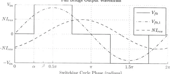
1-3 These plots demonstrate the operation of the full-bridge. The waveform
defi-nitions are shown in Figure 1-2. . . . . 20
1-4 These waveforms demonstrate the operation of the cycloconverter. The wave-forms are as defined in Figure 1-2. The phase shift,
#,
between Ies and VYc determines the power flow into the line. Vy is controlled by the cycloconverter sw itches. . . . . 212-1 Circuit diagram of the full-bridge inverter and a simplified model of the cy-cloconverter that is valid when the line voltage is positive. . . . . 26 2-2 These waveforms illustrate the cycloconverter being operated as a rectifier. . 27
2-3 Waveforms that demonstrate ZVS in the full-bridge. . . . . 30
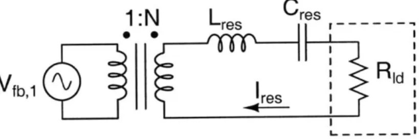
2-4 This is a simplified model of the inverter, which is true only when the cyclo-converter is operated as a rectifier. Vfb,1 is the fundamental of the full-bridge voltage, as shown in Figure 2-1 and calculated in Equation 2.1. Rld is the equivalent load resistance of the cycloconverter at a given average power level. 31
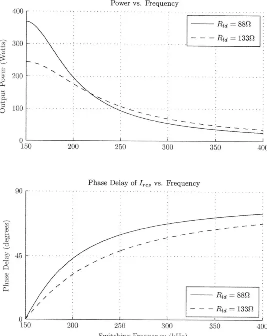
2-5 This plot shows how, at 75% (88Q) and 50% (133Q) average output power
levels, frequency affects the output power and the phase delay (/) of the resonant current relative to the fundamental full-bridge voltage. The chosen parameters are: 0 = 7, Cres = 7.5nF, Lre, = 150pH, V = 25V, N = 8. ... 32
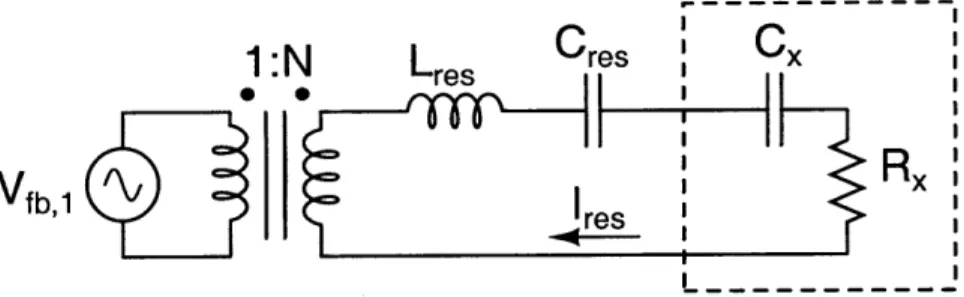
2-6 This is a more general version of the inverter model shown in Figure 2-4. This
model accounts for the reactive component in the equivalent load impedance when the cycloconverter is not behaving purely as a rectifier.. . . . ... 33
2-7 This plot shows how the load impedance varies with
#.
When#
= 0, the equivalent impedance is Z, = Rid. As#
approaches E, Z2 approaches 0.. . . 352-8 "Bumps" in resonant current amplitude occur when the maximum switching frequency is limited to 400kHz. Here, 0 is set to its minimim point (while still maintaining ZVS), in order to minimize switching frequency for a given output power, and all other parameters are the same as indicated in Figure 2-5. 36
3-1 Inductor parameters and image. . . . . 40
3-2 Transformer parameters, winding layout, and image . . . . 41
3-3 Picture of the prototype board, with important parts of the board labeled.
Note the two legs of the cycloconverter are indicated in two separate boxes. For initial, static input and output voltage testing, the negative leg (on the right) was shorted. The board is approximately 12"x8". . . . . 43
4-1 These oscilloscope screenshots illustrate the operation of the full-bridge. (a) corresponds to Figure 1-3 and shows the drain-source voltage of the low side FET in the leading leg (top waveform) and trailing leg (middle waveform). The bottom waveform is the differential voltage, Vfb, which is impressed on the primary of the transformer.
(b) corresponds to Figure 2-3 and shows the voltage across and current through
the secondary of the transformer (NVfb and Ires) This operating point illus-trates the full-bridge taking full advantage of PSPWM, while maintaining
ZVS. The ringing in the voltage waveform is discussed in Section 5.1.3. The operating parameters are: Vi=25V, Viine=240V, RI=133Q, f5.=211kHz,
4-2 These oscilloscope screenshots illustrate the operation of the cycloconverter. (a) corresponds to Figure 1-4. The square-wave signal is Vyc and the sinu-soidal signal is Ires, measured on the secondary side of the transformer. Here, IPP60R099 MOSFETs were used, and at this operating point the minimum phase shift to achieve ZVS is 380 given a dead-time of 750ns.
(b) demonstrates ZVS in the cycloconverter. The same Vy, signal is shown,
along with the gate-source voltages for the FETs in the positive cycloconverter leg. The low-side FET is not turned on until Vy has dropped all the way to
OV. Likewise, the high-side FET is not turned on until Vy has reached V1,.
The operating parameters for these waveforms are the same as in Figure 4-1. 50
5-1 This plot was taken from the IPP60R250 datasheet, and shows an approximate linear relationship between the energy stored in the output capacitance of the FET
List of Tables
1.1 CEC Weightings ... ... 19 2.1 Inductor Sizes . . . . 29 4.1 These measurements were taken with an input voltage of 25V. The approximated
CEC efficiency is 93.24%. The asterisks denote operating points that required too much current for the power supply. Values were plugged in that assumed the same efficiency as measured at the .257r phase point. Lres=165pH, Cres=13.2nF, N=8. . 52 4.2 These measurements were taken with an input voltage of 34V. The approximated
Chapter 1
Introduction
Renewable energy has become an important focal point for research at MIT, reflecting na-tional and internana-tional pressure to drive invention and innovation that will help to solve the world's energy woes. Solar power research has expanded considerably at MIT along with installed solar power capacity around the world. Between 2007 and 2008, world-wide grid-connected solar power capacity grew by more than 50% [4].
Harnessing solar power presents numerous technical challenges from a variety of fields, most notably physics, mechanical engineering, materials science, and electrical engineering. For electrical engineers, a primary challenge is converting the low voltage (-.5V) DC gener-ated by a typical silicon photovoltaic (PV) cell to the high voltage (-200V RMS) AC of a grid.
Part of the problem is solved simply by the packaging of PV cells. A solar module is a basic unit of purchase for a consumer who wishes to put together a PV installation. A module usually consists of 50 to 80 cells connected in series, encapsulated in glass, and held together with an aluminum frame. Because these cells are connected in series, a typical module operates at around 25-40V DC and generates around 175W of power.
In a typical solar installation, multiple modules are connected in series so that the total voltage of the string surpasses the peak line voltage. A switching inverter is then used to connect the entire string to the grid. These inverters, made by manufacturers such as Solectria, SMA, and Xantrex, are typically rated for 2-5kW output power and an input voltage of 200-500V.
1.1
Micro-inverters
A different approach involves connecting each module directly to the grid through its own
low-power, low-input-voltage inverter, or micro-inverter. The two approaches have several tradeoffs. Generally, inverters rated for higher power have better energy conversion efficiency. However, connecting one micro-inverter to each module improves peak power tracking and robustness to single module failures in an array. Micro-inverters may improve the overall energy output of an installation, even if their energy conversion efficiency is slightly worse than that of high-power inverters.
An example of a solar micro-inverter, manufactured by Enphase Energy, is pictured in Figure 1-1. The circuitry is encased in a small aluminum box, which attaches to a rack behind a solar module. The devices have three connections: two are AC connections to the grid so that the micro-inverters can be daisy-chained, and the third one is a DC connection to the panel. The devices communicate through the AC wiring to a central, internet-enabled box, which allows data about each panel to be gathered and accessed on the web.
This project involves the development of a next generation micro-inverter architecture, including the design, assembly, and testing of a prototype converter. The primary goal is to validate a conversion architecture that is well-suited to emerging trends in semiconductor devices in order to achieve improved efficiency.
1.2
CEC Efficiency
One of the most important metrics for the performance of a solar inverter is its California Energy Commission (CEC) efficiency rating. This number is a weighted sum of the energy conversion efficiency of an inverter over a broad range of operating points. The weightings are shown in Table 1.1. Seemingly, the weightings are chosen so that a higher CEC efficiency indicates a higher net energy production over the operating lifetime of the inverter. The weightings imply that a solar inverter generates most of its energy at around 50-75% of its peak power rating. An example commercial product is rated for a CEC efficiency of about
% Rated Power 10% 20% 30% 50% 75% 100%
Weighting Factor .04 .05 .12 .21 .53 .05
Table 1.1: CEC Weightings
94.5%. The goal of this project is to ultimately achieve 97% CEC efficiency. This thesis explores a topology that shows the potential to reach the target efficiency.
1.3
Topology
The chosen topology, shown in Figure 1-2, has two stages: a full-bridge series resonant inverter and a cycloconverter. To understand the intended operation of this circuit, a short description of the two stages follows.
VinH
0
0
Leading Leg Output Voltage (Vlead)
Trailing Leg Output Voltage (Vtraii)
0
in
0
Full Bridge Output Voltage (Vfb)
7 2- 37
Switching Cycle Phase (radians)
Figure 1-3: These plots demonstrate the operation of the full-bridge. The waveform defini-tions are shown in Figure 1-2.
1.3.1
Resonant Inverter
The four switches of the full-bridge are controlled to generate an output voltage as shown in Figure 1-3. The leading and trailing legs of the full-bridge are operated at 50% duty cycle, and the differential output voltage waveform is determined by the DC panel voltage,
Vin, and the phase shift angle between the two legs, 0. This control scheme is commonly known as Phase Shift Pulse Width Modulation (PSPWM). The full-bridge drives a series resonant tank and generates an approximately sinusoidal current oscillating at the switching
frequency.
1.3.2
Cycloconverter
A cycloconverter is used to convert the high-frequency current generated by the resonant
inverter to a much lower line-frequency current. The two switches that share a node with
V,± form the positive leg of the cycloconverter, and the two other switches form the negative
leg. When the line voltage is positive, the negative leg switches are closed, while the positive leg operates at 50% duty cycle. Likewise, when the line voltage is negative, the positive
Input Current (Ires)
Input Voltage (Vcyc)
Power
v;K I
0 .57r r 1.5r 2r Switching Cycle Phase (radians)
Figure 1-4: These waveforms demonstrate the operation of the cycloconverter. The wave-forms are as defined in Figure 1-2. The phase shift,
#,
between Ires and Vyc determines the power flow into the line. Vy is controlled by the cycloconverter switches.leg switches are closed, while the negative leg operates at 50% duty cycle. The phase shift angle (#) between the cycloconverter input voltage and the resonant current determines the power flow into the line. When full power delivery is required, the cycloconverter acts as a rectifier (# close to zero), delivering only positive or negative charge depending on the polarity of the line voltage. When zero power is required (corresponding to zero volts across the line),
#
is set to Z so that an average of zero charge is delivered during each switching2 cycle. The line voltage is approximated as constant during a switching cycle, because the switching frequency is three orders of magnitude greater than the line frequency.1.4
Important Characteristics
Several characteristics of this topology indicate that it can achieve the target of 97% CEC efficiency and meet necessary volume and weight standards. First, the circuit can be operated so that all switches are zero voltage switched (ZVS), effectively reducing switching loss to close to zero. ZVS requires that a switch turn on only when the body diode of the switch is
conducting. Since N-channel MOSFETs will be used as switches, the ZVS requirement will constrain the operation of the switches so that the current into the drain must be negative when the switch turns on.
Second, the losses mostly scale with output power. This is important because the CEC scaling dictates that efficiency remain relatively constant over a wide power range. In this circuit, as output power decreases, the RMS current in the circuit decreases, which also means that conduction losses decrease. Conduction losses are assumed to be a major component of the losses in the circuit.
Third, in order to keep the inverter relatively small and lightweight, the resonant tank and the transformer operate at high frequency. Line frequency magnetics are not an option because they would be too heavy, too costly, and take up too much space. This circuit does require an input capacitor sized for twice the line frequency, in order to maintain a steady voltage across the solar module despite varying output power over the course of a line cycle.
1.5
Specifications
The following target specifications are provided for the prototype. Note that the "maximum output power" specified is output power averaged over a line cycle.
Minimum Input Voltage 25V
Maximum Input Voltage 40V
Output Voltage 240V RMS
Maximum Output Power 175W
CEC Efficiency >97%
1.6
Organization
Chapter 2 will go into detail about the theory and high level design of the inverter. A preliminary control scheme will be presented. Based on the control scheme, a simplified sinusoidal steady-state model will be presented. The model will be used to derive conduction
losses and to calculate appropriate control signals for static operating points across a line cycle.
Chapter 3 will document the magnetics designs, switch selection, and the microcontroller-based setup that was used to generate the gating signals for the switches. Also, the procedure for taking measurements and the calculations for determining CEC efficiency will be pre-sented.
Chapter 4 will describe initial testing that was performed to help determine a control scheme. The control scheme will be discussed in detail, and CEC efficiency data points will be presented.
Chapter 5 will discuss the results and present recommendations for a path forward to achieve improved CEC efficiency.
Chapter 2
Theory and Control
The theoretical analysis of this circuit is based on an initial attempt at a high-efficiency control strategy. The control strategy is designed to minimize RMS currents in the circuit and thereby minimize conduction loss. The resonant inverter will modulate power over the course of a line cycle, and the cycloconverter will behave as a rectifier and unfolder, delivering all the power that it can to the line. This ensures that minimal excess current is supplied
by the resonant inverter, and minimal excess energy is sloshed around in the resonant tank.
Please note that for simplicity of language, "power delivered to the line averaged over a switching cycle" will be referred to as "instantaneous power", even though it is technically not instantaneous. Also, when a waveform is referred to in an equation, the amplitude of the waveform is the intended value, unless otherwise specified.
2.1
Resonant Inverter
This section will present a preliminary analysis of the voltage waveform that drives the resonant tank, a simple model of the cycloconverter, and logic behind the selection of several key parameters, including the transformer turns ratio and the resonant inductance.
Yline
Figure 2-1: Circuit diagram of the full-bridge inverter and a simplified model of the cyclo-converter that is valid when the line voltage is positive.
2.1.1
Full Bridge Voltage
To model the input to the resonant tank, only the fundamental component of the full-bridge voltage waveform is considered. The full-bridge is operated at a switching frequency above the resonant frequency of the tank so that the third, fifth, and higher harmonics of the square wave inputs can be disregarded. By superposition, the amplitude of the fundamental
(Vfb,1) can be expressed as a function of the DC panel voltage (Vi,) and the phase shift angle between the two legs of the full-bridge (0, as shown in Figure 1-3).
Vfb,l = !Vin|(1 - ejo)| = Vin sin 0 (2.1)
2.1.2
Equivalent Load
To simplify the analysis of the resonant inverter, the cycloconverter is modeled as an equiv-alent impedance at the fundamental switching frequency. The resonant inverter is expected to modulate current so that it scales linearly with the line voltage. If the cycloconverter acts as a rectifier (# = 0) delivering only positive current when the line voltage is positive
and negative current when the line voltage is negative, its equivalent impedance is purely resistive. Figure 2-4 shows an equivalent circuit model depicting this operating condition. In Figure 2-2, the fundamental of the input voltage to the cycloconverter (with the DC component included) is shown in dotted lines and has an amplitude of Vc,1 Vine, where
Vine is the instantaneous value of the line voltage at a point in the line cycle.
fun-Cycloconverter Voltage and Fundamental (Vc and V.c,1)
VI)',
U
Resonant Current (Ires)
0 I(e
Switching Cycle Phase (radians)
Figure 2-2: These waveforms illustrate the cycloconverter being operated as a rectifier.
damental of the input voltage and the input current, also referred to as the resonant current
(Ires).
S= Vcc,1Ires = "Vineires (2.2)
For a given average output power, an equivalent load resistance (Rid) defines the relationship between line voltage and instantaneous output power. To find Rid, the instantaneous power is defined as a function of the RMS of the fundamental of the voltage across Rid
(Vcyc,1,RMS)-p _cyc,1,RMS
Rid
2
V?
_2 line
Rid (2.3)
When the instantaneous line voltage is equal to the RMS of the line voltage (Vine,RMS)
average power over a line cycle (Paeg) is being delivered.
P 2
= b ine,RMs
Pavg - Rid(24
Thus, at the maximum average power of 175W into a 240V RMS line, Rid ~ 66Q.
2.1.3
Transformer
The transformer boosts the voltage at the output of the full-bridge so that it can meet the required voltage at the input of the cycloconverter. The worst case scenario occurs when the DC panel voltage is at its minimum, and the output line voltage is at the peak of the line cycle (Vline,peak). The full-bridge is assumed to be driving a full square wave (0 = 7r)
and operating at resonance so that the impedances of the resonant capacitor and inductor cancel. In practice, this is not an acceptable operating point, owing to the need for soft switching.
Under these conditions, the minimum voltage amplitude on the primary side of the transformer (VKri,min) and the maximum voltage amplitude on the secondary side of the
transfomer (Vsec,max) can be calculated. The minimum required turns ratio (Nmin) is:
Vpri,min = !Vi,min = A -25V ~_ 31.8V (2.5)
Vsec,max = IVine,peak = iv 2 - 240V ~' 216V (2.6)
Nmin Vsec,max 6.8 (2.7)
VPri,min
Based on these calculations, a conservative transformer turns ratio of N = 8 was chosen.
2.1.4
Resonant Inductor
The resonant inductor determines the quality factor of the resonant tank. A high quality fac-tor ensures that the resonant current is sinusoidal, because harmonics are heavily attenuated. The expression for quality factor in a series resonant inverter is:
Q =d (2.8)
From Equation 2.4, as average power output decreases, the equivalent load resistance in-creases, and the quality factor will decrease. This means that, for a given quality factor and resonant frequency, W0 = LC , the required resonant inductance increases as the aver-age power is reduced. Below a minimum averaver-age power, the cycloconverter can be used to
% Rated Power 10% 20% 30% 50% 75% 100%
Inductance (pH) 700 350 233 140 93 70
Table 2.1: Inductor Sizes
modulate power. The resonant inductor will determine this "average power sloshing bound-ary." (Discussion of the cycloconverter and its impact on the circuit when it modulates power will be saved for Section 2.3.)
Since the goal is to maximize the CEC efficiency of the circuit, which is a function of the efficiency at six average powers, there are six possible optimal inductances, where each inductance is associated with a sloshing boundary. A required quality factor of 1 was chosen based on qualititave observation of current waveforms in a SPICE simulation. Six possible inductor values (shown in Table 2.1) were calculated for an arbitrarily chosen resonant fre-quency of 150kHz. A program was written to develop six optimal circuits designed for the six possible sloshing boundaries. It accounted for inductor losses, as well as switch-related conduction and gating losses (see Section 2.4 and Appendix A). The best CEC efficiency resulted from setting the sloshing boundary at 50% power, so an inductor size of 150pH was chosen.
It should be noted that the resonant inductor can also be placed on the low side of the transformer. For a turns ratio of 8, the equivalent inductance would be reduced to 50pH, or 2.4pH. Initial attempts to design a low side inductor proved especially difficult because of the very small number of turns required and an associated lack of resolution, e.g. with an
AL value of 400 nH , 2 turns give 1.6pH, and 3 turns give 3.6pH.
2.2
Resonant Inverter Control
This section will focus on the control of the resonant inverter, which is mostly responsible for modulating instantaneous output power. The instantaneous output power can be controlled with two handles: phase shift in the full-bridge (#) and switching frequency (w). Before
Full Bridge Output Waveforms ./ . . ... .. . -- - N /~~~~~ ...-.--N ' Vf b, I 0/ 'V 0 7 0 5) 15w 2T
Switch ing Cycle Phase (radians)
Figure 2-3: Waveforms that demonstrate ZVS in the full-bridge.
2.2.1
Conditions for ZVS
Maintaining ZVS is essential because of the high efficiency requirement that the circuit is aiming to fulfill. In Figure 2-3, an example of the full-bridge in a ZVS mode is shown, where the waveform labels correspond to the labels in Figure 2-1. In the figure, 13 is the phase delay between the current and the fundamental of the full-bridge voltage, and aZ, which is a simple function of 0, marks the phase delay between the fundamental of the full-bridge
voltage and the turn-on of the high side switch in the leading leg. The constraint for ZVS is simply
#
> a. This constraint limits the extent to which the full-bridge can take advantage of PSPWM to lower the instantaneous output power of the inverter. The difference between3 and a will be referred to as the full-bridge ZVS phase margin, 6.
2.2.2
Frequency Control
Once the PSPWM limit has been reached, the instantaneous output power can be further reduced by increasing frequency. Figure 2-5 shows that as frequency increases,
#
increases, allowing us to safely increase a. Essentially, moving the frequency lever changes the limits on the PSPWM lever. The minimum frequency will be determined by the maximum power requirement. The transformer has been sized with enough margin that the circuit should never need to be operated very close to the resonant frequency. The maximum frequency limit will be discussed in Section 2.2.4.1:N
Lres
Cres---Vfb,1 RId
L...---I
Figure 2-4: This is a simplified model of the inverter, which is true only when the cyclocon-verter is operated as a rectifier. Vb,1 is the fundamental of the full-bridge voltage, as shown in Figure 2-1 and calculated in Equation 2.1. Rid is the equivalent load resistance of the cycloconverter at a given average power level.
2.2.3
Power Modulation
With the cycloconverter modeled as a resistor, determining how instantaneous power can be modulated by the resonant inverter becomes simple. The impedance of the resonant circuit shown in Figure 2-4 is:
1
Zres = Rid + LresjW + (2.9)
Cresjw
The resonant current driven into the load is:
Vf b,lN 44N V sin (210
-Tres = -'i = Va in s 2 (2.10)
Zres Rid + LresjW + c1s
Finally, power is given as a function of the resonant current:
I= es,RMsRId = 2I2esRld (2.11)
Note that these expressions are only valid when the cycloconverter is operated as a rectifier.
2.2.4
Maximum Frequency
The frequency lever does not have an upper limit that is as easy to define as the PSPWM limit. Inductors and switches are optimized for specific frequencies or ranges of frequencies, so the switching frequency will be limited. Above a specified frequency limit (or below the associated minimum power) the cycloconverter, which introduces a third lever, will be used
Power vs. Frequency Rld 88Q *R- - - d 133Q 400 300 200 100 0 -150 300 350 90 F...
Phase Delay of I .e vs. Frequency
0 '
150 200 250 300 350 400
Switching Frequency (kHz)
Figure 2-5: This plot shows how, at 75% (88Q) and 50% (133Q) average output power levels, frequency affects the output power and the phase delay (0) of the resonant current relative to the fundamental full-bridge voltage. The chosen parameters are: 0 = T, Cre = 7.5nF, Lres =
150pH, V, = 25V, N = 8.
200 250 400
1-N
L
res Cres rer'
CXAV I
1:N L
Ires
RFigure 2-6: This is a more general version of the inverter model shown in Figure 2-4. This model accounts for the reactive component in the equivalent load impedance when the cy-cloconverter is not behaving purely as a rectifier.
to modulate power. This frequency will be referred to as the "instantaneous power sloshing boundary."
2.3
Cycloconverter Analysis
The cycloconverter is responsible for modulating output power at low power levels (below the instantaneous and average power sloshing boundaries). The power delivered as a function of line voltage, resonant current, and cycloconverter phase shift (0 as defined in Figure 1-4) is:
I
= 2 j Vcc(t)Ires(t) dt = 7Vrne'res cos (2.12)In order to ensure ZVS, the voltage will lag the current, so the equivalent load impedance (Z,) now has a reactive component. This complex impedance is modeled by a capacitor (C with reactance Xx) in series with a resistor (Rx), as illustrated in Figure 2-6.
1
Z= Rx +jXx = Rx + . (2.13)
11 I(-Rx CxW)2+1 (2.14)
C1W
2.3.1
Impedance Trajectory
To make this complex impedance easier to understand, the trajectory of the impedance as
#
shifts from 0 to 2 will be derived. The magnitude of the load impedance defines the ratio2 of the fundamental cycloconverter voltage waveform to the resonant current.RZ1 cos=I= Vine (2.16)
Ires
From Equations 2.4 and 2.12:
Riacos#= ""re (2.17)
Combining this with Equations 2.14 and 2.16 results in:
cos
#
(RxCxw)2 +1 (2.18)RidCxw
This expression and Equation 2.15 reduce to the following pairwise relationships between
Xx, Rx, and #:
Rx Rid cos2
#
(2.19)X -Rld cos # sin # (2.20)
X = -1/ Rx( RId - R,) (2.21)
As shown in Figure 2-7, the impedance trajectory looks like a half circle, starting at Rid,
curving down to a minimum reactance, Xx = -R 1 when R - R=d and then curving back
2 x 2'7
to 0.
2.3.2
Further Analysis
Since the added capacitive component is in series, the new apparent resonant capacitance will decrease (Cres =
f"ecj)
and the resonant frequency and quality factor will increase.Furthermore, Rx will be a fraction of Rid, so the quality factor will increase further. This means that as
#
varies from 0 to{
4 radians, the resonant current is guaranteed to increase ifImpedance Trajectory Resistance R.
0 25Ri .5Rid .75Rid R1,
()
0I
-.5R1,1 \
Figure 2-7: This plot shows how the load impedance varies with
#.
When # = 0, theequivalent impedance is Z., = Rid. As
#
approaches !, Z. approaches 0.0 and w are kept constant.
For the operating point depicted in Figure 2-8, when
#
is very small, output power is actually greater than when#
= 0, because the resonant current magnitude increases at afaster rate than the decreasing "cos
#"
term in Equation 2.12. Theoretically,#
has to jump from 0 to some angle in order to maintain the relationship between output power and line voltage (Equation 2.4). This discontinuity is evident in the figure.2.4
Loss Calculations
The circuit design was optimized using a simple loss model that accounted for losses in the switches and the inductor.
2.4.1
Switch Losses
The circuit consists of eight MOSFETs: the four low voltage MOSFETs in the full-bridge, which must withstand the open circuit voltage of the panel, and the four high voltage MOS-FETs in the cycloconverter, which must withstand the peak line voltage. All MOSMOS-FETs are assumed to be zero voltage switched. The output capacitance keeps the drain-source voltage low while the switch turns off, and the switch waits to turn on until its body diode
Resonant Current over a Quarter Line Cycle 3.5 -3 .5 100% Power .5 -)-75% Power -- 50% Power 0 0 .25r 5
Line Cycle Phase (radians)
Figure 2-8: "Bumps" in resonant current amplitude occur when the maximum switching frequency is limited to 400kHz. Here, 0 is set to its minimim point (while still maintaining ZVS), in order to minimize switching frequency for a given output power, and all other parameters are the same as indicated in Figure 2-5.
is fully conducting. Theoretically, the only substantial losses are conduction loss due to the drain-source resistance (Rds) given an RMS current through the switch (Isw,RMS) and loss
associated with charging and discharging the gate given a gate charge (Qg), a gate-source voltage (Vg,), and a switching frequency in Hertz (fw). The expected average power loss in a single switch is:
Psw IswRus Rs + 2QgVgsfsw (2.22)
Low Voltage Switch Losses
For the four switches in the full-bridge, eight gate transitions occur per switching cycle, and two switches are conducting at all times (disregarding dead-time). The total loss in the full-bridge switches is based on the gate charge and drain-source resistance of the low voltage switches, Qg,jo and Rds,lo, respectively.
Psw,io = 2(1 NIres )2 Rs,Io + 8Qgiogsfsw (2.23)
High Voltage Switch Losses
In the cycloconverter, it can be approximated that the current always flows through 1.5 switches. When the positive leg switches are being switched at 50% duty cycle, the current can flow through both of the negative leg switches, which are held on. Only two switches at a time are operated at the switching frequency, which means that there are only four gate transitions per switching cycle in the cycloconverter. The total loss in the cycloconverter
switches is based on the gate charge and drain-source resistance of the high voltage switches,
Qg,hi and Rds,hi, respectively:
Psw,hi = 1.5( Ires )2 Rds,hi + 4Qg,hiVgsfsw (2.24)
2.4.2
Inductor Losses
Core Loss
The core loss was calculated from the Steinmetz parameters of the material. Our core choices were limited to commonly available ferrite materials (3F3, 3C96) and to the commonly avail-able cores (RM14, RM12, RM10). The parameters were taken from a supplier's application note [1]. The Steinmetz equation is of the form:
PL,core V k fa Beak (2.25)
PL,core is the loss in milliwatts, V is the core volume in cm3,
f
is the frequency of theinductor current in Hz, and Bpeak is the amplitude of the core flux density in Tesla. The three Steimetz parameters provided are k, a, and 3. The flux density is a function of the number of turns (NL), the effective core area in m2 (Ae), the resonant current through the
inductor, and the AL value ( nH ), which relates to the size of the gap.
Bpeak - AL -NL ' Ires (2.26)
109 -Ae
Winding Loss
Because of the need to maximize efficiency and because of the frequencies at which the circuit operates, the use of Litz wire is necessary. Litz wire mitigates the impact of skin effect and proximity effect in high frequency magnetics. A technique described by Gu and Liu was used to calculate the AC resistance (RL,AC) of an inductor that uses Litz wire [2]. The following equation shows winding loss associated with a constant resonant current.
PL,wind = (Ires,RMS)2RL,AC (2.27)
The details of the calculations can be found in the paper by Gu and in the code in Ap-pendix A.
Chapter 3
Prototype Implementation
This chapter will document the parts selection, board layout, and assembly of a prototype that was built to test the validity of the loss model. The test setup that was used to collect efficiency data will also be documented.
3.1
Switches
The two important parameters that were considered for MOSFET selection were the gate capacitance (Qg) and the drain-source resistance (Rd,). The product of Qg and Rd, were
used as a metric for initial switch selection. These two parameters are typically inversely proportional to each other. Intuitively, at higher relative switching frequencies, the gate capacitance has more impact on loss. Likewise, for higher relative RMS currents, the drain-source resistance is the primary loss mechanism. Switches available from popular suppliers (Digikey and Mouser) in popular footprints (TO-220 and D2PAK) were considered. The Qg and Rd, values for promising switches were plugged into a Python program (included in Appendix A). The program picked out switches that gave the best overall CEC efficiency.
3.1.1
Low Voltage Switches
The full-bridge switches need to withstand the voltage of the solar module. The maximum open circuit voltage is 60V, so switches with a minimum drain-source voltage rating of
75V were considered. STMicroelectronics MOSFETs (STB160N75F3) were used for the full
bridge. They have a drain-source voltage rating of 75V, a drain-source resistance of 3.2mQ, and a gate charge of 85nC.
3.1.2
High Voltage Switches
The cycloconverter switches need to withstand the peak line voltage as well as line tran-sients. MOSFETs with minimum drain-source voltage ratings of 600V were considered. The program picked out a variant of an Infineon 650V MOSFET. Initially, the IPP60R099 was used in the prototype, with an Rd, of 99mQ, and a Qg of 8OnC. For reasons discussed in
Sec-tion 4.1.2, the cycloconverter switches were changed to IPP60R250, with an Rd, of 250mQ, and a Qg of 26nC.
3.2
Inductor
Core RM14 Material 3F3 Gap 3.6mm Turns 44 Litz gauge 44 Litz strands 243 Inductance 165pH (a) (b) (C)Figure 3-1: Table (a) enumerates the design details of the inductor. Figure (b) shows a cross section of the winding area. The left edge is closest to the center of the bobbin. Insulative tape was used to keep windings out of the center region close to the gap. Figure (c) is a picture of the inductor.
The Python program was able to generate preliminary inductor designs, however they turned out to be unrealistic, because the simulated packing factor was too high. Donny Zimmanck of Dartmouth provided us with the final designs for both the inductor and the transformer. The designs were constrained to use Litz wire and cores made of 3F3 material
already available at MIT. The winding consisted of 3 lengths of 3x27x44AWG Litz wire braided together. The RM14 core has a 3.6mm air-gap, which results in significant fringing fields near the gap. The fringing fields aggravate the proximity effect in windings that are close to the gap [3]. In order to minimize this effect, before the inductor was wound, 10mm-wide insulating tape was wrapped around the center of the bobbin until the tape reached a thickness of 2mm. The tape forces more space between the windings and the gap.
3.3
Transformer
Core RM14 Material 3F3 Gap 0mm Litz gauge 408
o Primary turns 4 Primary strands 600 H Secondary turns 32 Secondary strands 80 (a) (b) (c)Figure 3-2: Table (a) enumerates the design details of the transformer. Figure (b) shows a cross section of the winding layout. The left edge is closest to the center of the bobbin. Figure (c) is a picture of the transformer that shows where the primary connections come out of the core.
The 1:8 transformer was designed to handle a peak magnetic flux of -100[pV-s on the primary. It is made out of an ungapped core, in order to minimize the amount of stored energy. The secondary winding was split into two winding windows to reduce losses asso-ciated with the proximity effect. Because of the significant voltage difference between the two windings, the primary winding was completely wrapped in Kapton tape. The primary is made of 15 lengths of 40x40AWG Litz wire that were twisted together. The secondary is made of 2 lengths of 40x40AWG Litz wire.
3.4
Prototype Board
The prototype board was designed with flexibility in mind by Brandon Pierquet of MIT. The digital signals to the gate drivers are controlled through headers that could be connected to any control interface. Extra pads and foot prints were placed to allow for differently sized inductors and resonant capacitances.
The board's design also reflects effort to minimize electromagnetic noise and ringing caused by parasitic inductances. The gate drivers are placed as close as possible to the switches to control gate voltage ringing at the transitions. High frequency capacitors rated for appropriate current ripple were placed in close proximity to each leg of the full-bridge in order to hold DC voltages constant and minimize ringing of MOSFET drain-source voltages. This board was also meant to test circuitry developed by Aleksey Trubitsyn of MIT for measuring the amount of charge delivered by a leg in a single switching cycle. This involved testing a shunt and a current transformer as two different methods for measuring current. In short, the measurement circuit involves an integrator, two sample holds, and an ADC, along with other digital circuitry for generating timing signals. The measurement circuitry is located below the transformer, shown in Figure 3-3.
3.5
Control Interface
In Chapter 2, three control levers were discussed: frequency (w), phase shift between the full-bridge legs (0), and phase shift between the cycloconverter input voltage and the resonant current (#). The position of these levers is decided by the gating signals that control the MOSFETs. A microcontroller was used to generate these gating signals, because they are easy to reprogram with a computer, and the wiring can easily be reconfigured with commonly available development boards.
The Atmel AT90PWM316 microcontroller, along with the STK500 development board, and the STK520 extension kit were used. The microcontroller is operated at 16MHz, but it also comes with a 64MHz Phase Locked Loop, which is used to generate a higher frequency clock input to the three "Power Stage Controllers" (PSCs). A PSC is a digital waveform
Figure 3-3: Picture of the prototype board, with important parts of the board labeled. Note the two legs of the cycloconverter are indicated in two separate boxes. For initial, static input and output voltage testing, the negative leg (on the right) was shorted. The board is approximately 12"x8".
controller that can be programmed to generate gating signals. With a 64MHz clock driving the PSCs, the frequency resolution at 200kHz is around 630Hz per step, and the phase shift resolution is 1.10 per step. The microcontroller code, included in Appendix B, was written to set up the necessary gating signals for a static operating point given three values, one value per control lever. The calculations to determine the appropriate microcontroller values are discussed in Section 4.2.
3.5.1
Dead-time
Dead-time is a small time period (relative to the switching period) during which both switches in a leg are off. Sufficient dead-time is a prerequisite for ZVS. The dead-time is set so that there is enough time for the body diode of a MOSFET to start conducting before the switch turns on. If the dead-time is too short, the switch turns on while there is still voltage across the diode, which will result in switching losses. If the dead-time is too long, there is unnecessary loss caused by the forward voltage drop across the body diode, which would be mostly eliminated if the switch were on.
In the experimental setup, dead-times could be adjusted by potentiometers on a small, simple daughter board. The board took as input a 50% duty cycle signal directly from the microcontroller. The rising edges of this input signal and its inverse were delayed through the use of RC low pass filters and a digital buffers, effectively generating gating signals for the top and bottom switches of a leg. A potentiometer adjusted dead-time for a gate signal
by altering the RC time constant of the corresponding low pass filter.
Because of the multitude of static operating points to test, it was not practical to manually adjust dead-times at each operating point. As a result, all dead-times were kept constant for the duration of the tests. The dead-time for the leading leg of the full-bridge was 225ns, for the trailing leg of the full-bridge, 275ns, and for the cycloconverter, 500ns. The dead-time for the trailing leg is slightly shorter than that of the leading leg because the transitions in the trailing leg often occur during a period of very high current. To mitigate losses associated with this transition, a Schottky diode (Diodes Inc. B180-13-F) was placed across the drain and source of both MOSFETs in the trailing leg.
3.6
Experimental Setup and Procedure
This section will document the experimental setup and methods that were used to make the measurements discussed in Chapter 4.
3.6.1
Power Supplies and Loads
In place of a solar module, two Agilent 6643A power supplies were wired in parallel. Each supply is rated for 35V at 6A. This limited our ability to test at the maximum 40V input voltage. This also limited our ability to test at the absolute peak input current of 14A, given a 25V input at 350W. However, most of the operating points could be tested with this setup.
To test static line voltages, the following active loads were used: an Agilent 6063B rated for 240V and 250W and an Agilent 6050A, which contains three 60V, 600W active loads. All of the power channels were wired in series in order to allow testing at the peak line voltage (~340V).
3.6.2
Efficiency Measurements
For simplicity, the circuit was tested at static operating points, where each point is defined
by an input voltage, an average output power, and a point in the line cycle. At each
static operating point, four raw measurements were taken: input voltage, input current, output voltage, and output current. The input voltage measurement was taken from the power supply display, after verifying the reading with a high precision multimeter. The input current was determined by using an HP 34410A multimeter to measure voltage across a precision 0.1Q shunt. The output voltage and output current were both measured by HP 34401A's. The voltage readings are 0.1% accurate, and the current readings are 0.5% accurate. These measurements do not take into account the gating losses, since the 12V gate drive circuitry was powered by a separate supply.
3.6.3
Efficiency Calculations
Efficiency (E) at a particular input voltage and average output power is a function of input energy over a line cycle (Ec,i,) and output energy over a line cycle
(E,st).
e = 'C'"" (3.1)
Eze,in
Energy over a line cycle (Ec) is estimated from a trapezoidal integral of instantaneous power at four equally-spaced phase points in a quarter line cycle (.1257r, .257r, .3757, and
.57 radians).
Eic = P 2 5r + P25 r + P3757 + .5P5 (3.2)
This calculation generates a value that is proportional to energy.
For a given input voltage, the inverter was tested at 100%, 75%, 50%, and 30% rated average power (since these are operating points that the CEC cares about). The efficiencies at 20% and 10% rated average power account for only 9% of the overall CEC efficiency, and for simplicity, the efficiency at these points was assumed equal to the efficiency at 30% rated average power (i.e. the efficiency at 30% rated average power accounted for 21% of the total
CEC efficiency).
Total CEC efficiencies were calculated for input voltages of 25V and 34V. The 34V limit was imposed by the power supply. Otherwise, efficiencies for an input voltage of 40V would be measured in order to test the full range of input voltages according to the specification.
Chapter 4
Testing and Results
This chapter will be divided into three sections. The first section will describe initial testing that led to some modifications to the circuit and the development of a control scheme. The second section will describe the control scheme and the algorithm that was used to generate the control values at the operating points enumerated in Section 3.6. The last section will
present a set of results for the design as of this writing.
4.1
Initial Testing
The control scheme for the inverter was guided by preliminary tests that were performed as the inverter was brought to full operation.
4.1.1
Minimizing Switching Frequency
The first aspect of the control scheme was determined from efficiency measurements that were taken while driving a resistive load (in place of the cycloconverter) with the resonant inverter. Current through the resistor was measured with a current probe connected to an oscilloscope. The resistances tested were 66Q, 100Q, and 133Q, which correspond to 100%,
66%, and 50% average output powers, respectively.
The first set of efficiency measurements were taken with a fixed full-bridge phase shift
01""""""r~~" .N....4",
1 2OO0' z5.C5/ o~ V .Op 172V 100 10y cops0
(a) (b)
Figure 4-1: These oscilloscope screenshots illustrate the operation of the full-bridge.
(a) corresponds to Figure 1-3 and shows the drain-source voltage of the low side FET in the leading leg (top waveform) and trailing leg (middle waveform). The bottom waveform is the differential voltage, Vfb, which is impressed on the primary of the transformer.
(b) corresponds to Figure 2-3 and shows the voltage across and current through the
sec-ondary of the transformer (NVfb and Ires) This operating point illustrates the full-bridge
taking full advantage of PSPWM, while maintaining ZVS. The ringing in the voltage wave-form is discussed in Section 5.1.3.
The operating parameters are: XKn=25V, Vine=240V, Rld=133Q, fam=211kHz, 0=100'
Cres=13.2nF, Lres=165pH, N=8.
followed by tests wherein the circuit was controlled to take advantage of PSPWM, which has the affect of reducing the switching frequency at a given output power. The ZVS phase margin (6, from Section 2.2.1) was fixed at 100, and the same operating points were tested. Efficiency improved across the board at the lower switching frequencies. In cases where the switching frequency was drastically reduced, efficiency jumped by up to 4% at a given output power into a given load.
4.1.2
Cycloconverter Adjustments
After these preliminary tests, the cycloconverter was installed and tested. It was immediately discovered that the ZVS condition requires a substantial phase shift (4) between the resonant current and the fundamental of the cycloconverter voltage.
At a given line voltage, a certain amount of charge is required to turn on the body diode of one switch in a leg and turn off the body diode of the other switch in the same leg
(i.e. to charge and discharge the device capacitances). This fact was ignored in the initial computations. In order to achieve a ZVS transition, this charge must be delivered by the resonant current within the dead-time. Ensuring adequate dead-time is extremely important, because hard switching results in disruptive noise and substantial switching losses. If
#
is small, the current at transition time will be small, and a long dead-time will be required. If#
is larger, the current at transition time will be larger, and the required dead-time will be shorter.With the IPP60R099 MOSFET and a configured dead-time of 500ns, the typical mini-mum phase shift was 400. This substantial phase shift motivated the search for a similar FET with a lower charge requirement for the body diode transitions, even though such a FET is expected to have a higher Rd,. Lowering the charge requirement will reduce the minimum
#
and reduce the resonant current needed (see Section 2.3). Reducing the resonant current will reduce conduction losses in the entire circuit, while increasing Rd,,hi will only impact the cycloconverter switches. With the IPP60R250 and the same dead-time of 500ns, the typical minimum#
was only 20'. The installation of these new switches improved the efficiency at all tested operating points by 1-2%.4.2
Control Scheme
The initial testing discussed above resulted in a Matlab script (included in Appendix C) to calculate a table of control values to be coded into the microcontroller for each static operating point. For all combinations of input voltage, average output power, and line cycle phase, the script numerically calculates the necessary switching frequency and the phase difference between the full-bridge legs. The script assumes a constant
#
of 10' and a fixed6 of 10' to ensure ZVS, while minimizing switching frequency. The algorithm increments
through all frequencies that the microcontroller can generate and performs the following calculations at each frequency f8,:
1. Calculate C2 and R. based on average output power, f,,, and
#
= 10'.(a) (b)
Figure 4-2: These oscilloscope screenshots illustrate the operation of the cycloconverter. (a) corresponds to Figure 1-4. The square-wave signal is VYc and the sinusoidal signal is
Ires, measured on the secondary side of the transformer. Here, IPP60R099 MOSFETs were used, and at this operating point the minimum phase shift to achieve ZVS is 380 given a dead-time of 750ns.
(b) demonstrates ZVS in the cycloconverter. The same Vy signal is shown, along with the
gate-source voltages for the FETs in the positive cycloconverter leg. The low-side FET is not turned on until Vy has dropped all the way to OV. Likewise, the high-side FET is not turned on until Vy has reached VM.