HAL Id: hal-03015612
https://hal.archives-ouvertes.fr/hal-03015612
Submitted on 19 Nov 2020
HAL is a multi-disciplinary open access
archive for the deposit and dissemination of
sci-entific research documents, whether they are
pub-lished or not. The documents may come from
teaching and research institutions in France or
abroad, or from public or private research centers.
L’archive ouverte pluridisciplinaire HAL, est
destinée au dépôt et à la diffusion de documents
scientifiques de niveau recherche, publiés ou non,
émanant des établissements d’enseignement et de
recherche français ou étrangers, des laboratoires
publics ou privés.
Engineering Optically Switchable Transistors with
Improved Performance by Controlling Interactions of
Diarylethenes in Polymer Matrices
Lili Hou, Tim Leydecker, Xiaoyan Zhang, Wassima Rekab, Martin Herder,
Camila Cendra, Stefan Hecht, Iain Mcculloch, Alberto Salleo, Emanuele
Orgiu, et al.
To cite this version:
Lili Hou, Tim Leydecker, Xiaoyan Zhang, Wassima Rekab, Martin Herder, et al.. Engineering
Opti-cally Switchable Transistors with Improved Performance by Controlling Interactions of Diarylethenes
in Polymer Matrices. Journal of the American Chemical Society, American Chemical Society, 2020,
142 (25), pp.11050-11059. �10.1021/jacs.0c02961�. �hal-03015612�
Engineering optically switchable transistors with improved performance by controlling interac-tions of diarylethenes in polymer matrices
Lili Hou,
†, #Tim Leydecker,
†Xiaoyan Zhang,
†,#Wassima Rekab,
†Martin Herder,
§Camila Cendra,
‡Stefan Hecht,
§,¶Iain McCulloch,
‖Alberto Salleo,
‡Emanuele Orgiu,
†,ǂ,*Paolo Samorì
†,*AUTHOR ADDRESS † Université de Strasbourg, CNRS, ISIS, 8 alleé Gaspard Monge, 67000 Strasbourg, France. § Department of Chemistry & IRIS Adlershof, Humboldt-Universität zu Berlin, Brook-Taylor-Str. 2, 12489 Berlin, Ger-many. ‡ Department of Materials Science and Engineering, Stanford University, Stanford, California 94305, USA. ¶ DWI - Leibniz Institute for Interactive Materials & Institute of Technical and Macromolecular Chemistry, RWTH Aa-chen University, Germany ‖ Department of Chemistry and Centre for Plastic Electronics, Imperial College London, London SW7 2AZ, United King-dom & Physical Sciences and Engineering Division, KAUST Solar Center (KSC), King Abdullah University of Science and Technology (KAUST), KSC Thuwal 23955-6900, Saudi Arabia.
ǂ INRS-Centre Énergie Matériaux Télécommunications, 1650 Blv. Lionel-Boulet, J3X 1S2 Varennes, Quebec, Canada # Present address: Department of Chemistry and Chemical Engineering, Chalmers University of Technology, Kemigården 4, SE-412 96, Gothenburg, Sweden. ABSTRACT: The integration of photochromic molecules into semiconducting polymer matrices via blending has recently at-tracted a great deal of attention, as it provides the means to reversibly modulate the output signal of electronic devices by using light as a remote control. However, the structural and electronic interactions between photochromic molecules and semiconducting polymers is far from being fully understood. Here we perform a comparative investigation by combining two photochromic diarylethene moieties possessing similar energy levels yet different propensity to aggregate with five proto- typical polymer semiconductors exhibiting different energy levels and structural order, ranging from amorphous to semicrys- talline. Our in-depth photochemical, structural, morphological and electrical characterization reveals that the photorespon-sive behavior of thin-film transistors (TFTs) including polymer/diarylethenes blends as the active layer is governed by a complex interplay between the relative position of the energy levels and the polymer matrix microstructure. By matching the energy levels and optimizing the molecular packing, high-performance optically switchable organic thin-film transistors were fabricated. These findings represent a major step forward in the fabrication of light-responsive organic devices.
INTRODUCTION
Photochromic molecules have garnered increasing atten- tion as building blocks for applications in artificial molecu-lar machines, data storage, imaging, and sensing.1 Amongphotochromic molecules, diarylethenes (DAEs) are ex-tremely interesting since they combine high fatigue re-sistance and thermal stability of the open and ring-closed configurations.2 Moreover, the two isomers possess
significantly different energy levels of their frontier molec-ular orbitals, i.e. the highest occupied molecsignificantly different energy levels of their frontier molec-ular orbital (HOMO) and the lowest unoccupied molecular orbital (LUMO). The associated ability to control this property change has been key to develop multifunctional organic de-vices, which just as conventional organic devices, are based on materials that can be solution-processed and, as such, are suited for roll-to-roll printing on flexible substrates at large scale.3 DAEs represent ideal systems to be combined
with organic/polymer semiconductors in order to reversi-bly tune the output current, conductivity, or electrolumi-nescence upon irradiation at distinct wavelengths.4 The use
of external light stimuli provides precise temporal and spa-tial control on the DAEs embedded in electronic material systems and devices thereof.
A simple-yet-effective approach to introduce optical
switching functions into organic devices consists in the di- rect blending of DAEs with organic semiconductors as ac-tive materials in the devices. Optically switchable organic thin-film transistors (OTFTs) have been fabricated by blending DAEs with different semiconductor matrices in-cluding poly(3-hexyl-thiophene) (P3HT), 2,7-dialkyl-ben-zothieno(3,2-b)benzothiophene (BTBT) or fullerenes.5 The
output current of these OTFTs could be controlled by choos-ing specific irradiation wavelengths. Moreover, poly- mer/DAE blends have been proven to be the key to fabri-cate flexible non-volatile optical memories exceeding 8-bit storage capacity.6
In order to design and optimize the materials for high-performance light-responsive multifunctional optoelec- tronic devices, it is highly desirable to gain an in-depth un- derstanding over the relationship between polymer struc- ture, photoswitching performance of DAEs, and the result-ing electrical properties of devices using such bi-component films as the active layer. More specifically, fundamental questions need to be addressed, such as: (i) how the pho-toisomerization process of a given DAE molecule is affected by the surrounding semiconducting polymer matrix; (ii) how the polymer packing itself is affected by the presence of DAEs, and (iii) what are the principles governing device mobility and optical switching in the devices based on the composition and processing of polymer/DAE binary blends.
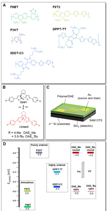
To address these open questions, we synthesized two DAEs, i.e. DAE_Me and DAE_tBu (Figure 1B), possessing very
2
closed isomers, respectively, Figure 1D) yet different side chains, the latter ruling the supramolecular interaction with the semiconducting polymers. In particular, the steric hin- drance brought into play by the four bulky tert-butyl sub-stituents of DAE_tBu leads to a lower tendency for both ag-gregation and association with the polymer matrix when compared to DAE_Me, which only has two pending methyl substituents. Moreover, five archetypal high-mobility p- type polymers (Figure 1A) were chosen that feature differ-ent HOMO levels (Figure 1D) and propensity to undergo self-assembly forming well-distinct morphologies. In par-ticular, poly(9,9-dioctylfluorene-alt-benzothiadiazole (F8BT)7 and poly(9,9-dioctylfluorene-alt-bithiophene)
(F8T2)8 form completely amorphous structures, whereas
thermally untreated P3HT organizes into poorly ordered films,9 and diketopyrrolopyrrole thieno[3,2-b]thiophene
copolymer (DPPT-TT)10 and
poly(4-decyltetradecylisoin-digo-alt-dithiophene) (IIDDT-C3)11 are known to generate
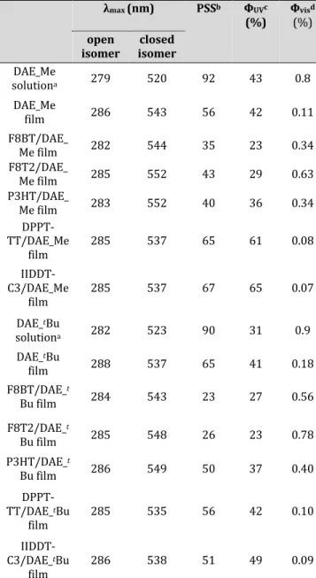
highly ordered semi-crystalline structures when thermally annealed. The photochemical properties of the DAEs em-bedded in the polymer matrices were studied by UV/visible absorption spectroscopy. The morphology of the poly- mer/DAE films was investigated by Atomic Force Micros- copy (AFM), whereas the structure was elucidated via graz- ing incidence wide-angle X-ray scattering (GIWAXS) meas-urements. OTFTs devices (Figure 1C) were fabricated and tested in order to characterize charge transport and light response of these ten polymer/DAE blends. By correlating the intrinsic electronic structure (i.e., energy levels) and matrix microstructure resulting from supramolecular inter-actions with the photochemical and electrical performance of polymer/DAE blends, we have gained insight into how to maintain the strong electrical performance of the semicon- ducting polymers while aptly exploiting DAE photoswitch-ing to fabricate efficient light-tunable organic devices. RESULTS Photochemical properties. The photoswitching behav- ior of neat DAEs and their blends with the chosen semicon- ducting polymers was studied by UV/vis absorption spec-troscopy. The open isomers of DAEs undergo ring closure (photocyclization) upon brief UV irradiation (312 nm, 35 s, 2.5 mW/cm2 ) in 1,2-dichlorobenzene (DCB), leading to for-mation of a new broad absorbance band between 400 nm and 650 nm for both DAE_Me and DAE_tBu (Figure S1). The conversion to the closed isomer in the photostationary state (PSS) upon UV irradiation reached 92% for DAE_Me and 90% for DAE_tBu.5b
Subsequent irradiation of this PSS with visi-ble light converts the closed isomer back to the open one (photocycloreversion), resulting in recovery of the initial spectra. The photocyclization and photocycloreversion of DAE_Me and DAE_tBu show relatively good fatigue
re-sistance, with < 20% loss of photochromic material over 8 illumination cycles in solution.5b
To gain further insight into the photochemical processes of DAEs when embedded in the polymer matrices, samples were prepared by spin-coating bi-component poly-mer/DAE solutions at concentrations of 2 mg/mL for the polymer and 0.5 mg/mL for the DAE, providing films with thicknesses between 20 nm and 30 nm. No further thermal annealing treatment was applied, except in the cases of DPPT-TT and its DAE blends, in which the spin-coated films
were annealed at 90 °C to improve microstructural order-ing.10a, 10c The weight ratio of DAEs in the blends was always
20 wt% in this study, in agreement with previous works which suggested that this percentage results in a good bal-ance between current modulation and device mobility in OTFTs.5a
Figure 1. Chemical structures of semiconducting polymers and
DAEs, resulting OTFT devices, and energetics. (A) Chemical structures of semiconducting polymers F8BT, F8T2, P3HT, DPPT-TT, and IIDDT-C3. (B) Molecular structures of pho-toswitchable DAE_Me and DAE_tBu in their open and closed
isomers, which can be interconverted reversibly by irradiating with UV or visible light. (C) Structure of the OTFT device ap-plied. (D) The HOMO energy levels of organic semiconducting polymers and DAEs used. 5a, 5b, 10a, 10b, 11b, 12. The comparative study on the photocyclization and pho- tocycloreversion of DAEs when embedded in the five cho-sen polymer matrices was carried out by exploiting the same irradiation power and distance as DAEs in solution, by simply varying irradiation time to confirm that the PSS is
3
reached in all the polymer/DAE blends. UV irradiation in-duced an increase in the absorbance between 400 nm and 650 nm in all five polymer matrices (Figure 2, and differ-ence spectra in Figure S2), indicating the formation of the closed isomer. After reaching the PSS, irradiation of the sample with visible light led to recovery of the initial spec- tra as a result of the DAE ring opening. The reversible pho-toisomerization was observed in both DAE_Me- and DAE_t
Bu-containing polymer matrices. The recorded spec-tra did not show any significant shift of the main absorption band of all five polymers upon blending with the DAE mol-ecules (see Figure S3). The photochemical properties of the DAE derivatives in polymer matrices are summarized in Ta-ble 1, including the spectroscopic characteristics of neat DAEs in solution and thin film as well for comparison pur-poses. The open isomer shows a very small bathochromic shift of λmax (< 7 nm) from solution to polymer matrices,
providing evidence for the absence of strong interactions between each polymer and the open DAEs in the ground state. A larger bathochromic shift of λmax
> 20 nm was ob-served for the closed isomers when embedded in amor-phous (F8T2, F8BT) and poorly ordered (P3HT) polymers, thereby suggesting that the electronic structure of the more planar closed isomers is perturbed by the polymer matri-ces.13 Conversely, polymer matrices with increased degree of ordering (IIDDT-C3 and DPPT-TT) induced a somewhat smaller bathochromic shift ofmax < 17 nm. The PSS of DAEs in thin films is considerably lower than in solution. The ring-open isomer of DAE adopts an approx-imate 1:1 mixture of parallel and antiparallel conformations, which can easily interconvert in solution, while only the an-tiparallel conformer undergoes photocyclization.2 However, when DAEs are deposited into films, the parallel conformer of the ring-open DAE is somewhat trapped and not enabled to convert to the photo-active antiparallel isomer, therefore the PSS is reduced as we observed. The PSS of DAEs also shows dependence on the microstructure of the polymer matrices. In the case of DAE_Me, the PSS of 67% in IIDDT-C3 and 65% in DPPT-TT decreased to 35% in F8BT, 43% in F8T2 and 40% in P3HT. For DAE_tBu, the PSS of 51% in
IIDDT-C3 and 56% in DPPT-TT decreased to 23% in F8BT, 26% in F8T2 and 50% in P3HT. The higher PSS in highly or-dered matrices might be attributed to the fact that a more ordered matrix can lead to a higher population of the anti- parallel conformation of the ring-open isomer, thus result-ing in a higher quantum yield for ring-closure. Furthermore, the PSS of DAE_tBu is lower than the PSS of DAE_Me in all polymer matrices (except in the case of P3HT) despite the similar value in solution phase, possibly due to the more sterically demanding DAE_tBu, the isomerization requires
more space to take place, which is hindered by the interac- tion with the surrounding matrix. The glass transition tem-perature of P3HT (Tg = 12 °C) is lower than the one of F8T2 and F8BT (70 – 130 °C),15c indicating a more flexible inner space of the amorphous region of P3HT at room tempera-ture, which may determine the moderate effect on the pho-toisomerization processes of DAE_tBu. Figure 2. UV/visible absorption spectra of polymer/DAE films and the photostationary state (PSS) upon UV light irradiation (312 nm) and visible irradiation. (A) F8BT/DAE_Me and F8BT/DAE_tBu films. (B) F8T2/DAE_Me and F8T2/DAE_tBu
films. (C) P3HT/DAE_Me andP3HT/DAE_t
Bu films. (D) DPPT-TT/DAE_Me and DPPT-TT/DAE_tBu films. (E)
IIDDT-C3/DAE_Me and IIDDT-C3/DAE_tBu films.
In order to quantify the efficiency of the DAEs pho-toswitching in the polymer matrices, the isomerization quantum yields under UV and visible light irradiation (ФUV
and Фvis
) were determined, and the results are also summa-rized in Table 1. ФUV is 50% for DAE_Me and 31% for DAE_
tBu in solution, respectively,5b and the neat DAE_Me and
DAE_tBu films show very similar values. The efficient ФUV
can be attributed to the practically barrier-less reaction pathway after excitation.14 When blended with polymers,
ФUV of DAEs is strongly affected by surrounding polymer
matrices. Highly ordered polymers have ФUV that about
double of those in amorphous polymers (e.g., ФUV = 61% for
4
more ordered matrix leads to a higher population of the an-tiparallel conformation of the ring-open isomer, only the antiparallel conformation can undergo ring closing while the parallel conformation cannot, and thus a higher quan-tum yield is observed in DPPT-TT and IIDDT-C3. Table 1. Photochemical properties of DAEs in solution and in polymer matrices. λmax (nm) PSSb ФUVc (%) Ф(%) visd open
isomer isomer closed
DAE_Me solutiona 279 520 92 43 0.8 DAE_Me film 286 543 56 42 0.11 F8BT/DAE_ Me film 282 544 35 23 0.34 F8T2/DAE_ Me film 285 552 43 29 0.63 P3HT/DAE_ Me film 283 552 40 36 0.34 DPPT-TT/DAE_Me film 285 537 65 61 0.08 IIDDT-C3/DAE_Me film 285 537 67 65 0.07 DAE_tBu solutiona 282 523 90 31 0.9 DAE_tBu film 288 537 65 41 0.18 F8BT/DAE_t Bu film 284 543 23 27 0.56 F8T2/DAE_t Bu film 285 548 26 23 0.78 P3HT/DAE_t Bu film 286 549 50 37 0.40 DPPT-TT/DAE_tBu film 285 535 56 42 0.10 IIDDT-C3/DAE_tBu film 286 538 51 49 0.09 a In acetonitrile. b Amount of the closed DAE isomer in PSS upon UV irradiation (312 nm), obtained by UV/vis absorption spectra with the experimental error of 10%. c Quantum yields upon 310 nm irradiation with the experimental error of 10%.
d Quantum yields upon 530 nm irradiation with the
experi-mental error of 10%.
As commonly observed in DAE photoswitches, visible light-induced ring-opening of the closed isomer is typically associated with a lower Фvis as a result of an energy barrier
along the excited state pathway.14 A reduction in Фvis was
observed in both the neat DAEs films and polymer blended films. F8T2/DAE films have the highest Фvis, with 0.63% for
DAE_Me and 0.78% for DAE_tBu. Фvis is slightly smaller in
P3HT and F8BT matrices (ranging between 0.34% and 0.56%). It should be noted that Фvis of DAEs in F8T2, P3HT
or F8BT are more than three times higher than those of neat DAEs in the solid state, reflecting the fact that the conforma- tional freedom in the matrices of these three polymers al-lows relatively unrestricted movement during the ring-opening process. For DPPT-TT and IIDDT-C3, Фvis are much
lower, below 0.1%, which can be attributed to steric hin- drance brought into play by the rigid polymer matrix im-peding the recovery of the open form. In general, DAE_tBu
shows slightly larger Фvis than DAE_Me in polymer matrices,
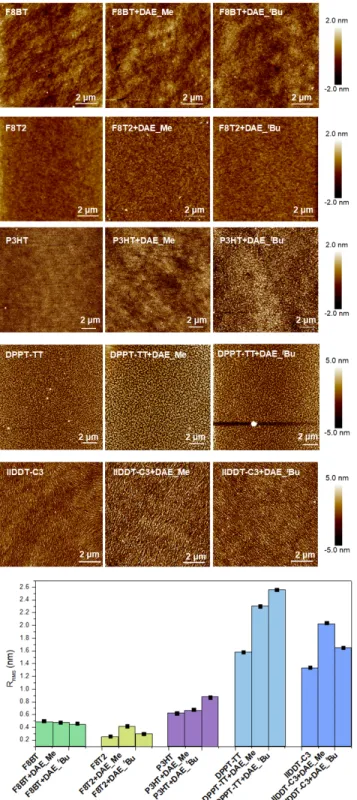
possibly due to the four bulky tert-butyl groups of DAE-tBu preventing deep interactions with the polymer microstruc-ture therefore less affecting the photocycloreversion. Morphology. As in a bottom-gate bottom-contact OTFT the charges mostly flow close to the interface between the sem-iconducting material and dielectric substrate, the surface morphologies in thin-films of polymer/DAE blends strongly affect the charge transport in the OTFTs applications.9b, 15
Atomic force microscopy (AFM) was used to study the mor- phology of neat polymers and polymers/DAE films. The im- ages displayed in Figure 3 are discussed based on the ap-peared morphological features and on the root-mean-squared (RRMS) roughness, which was estimated on region of 10×10 µm2. On the tens of micrometers scale explored by AFM, the binary films did not exhibit significant phase sep-aration between the polymer and DAE component forming the blends, highlighting a good miscibility for both DAE_Me and DAE_t Bu when blended with all the five chosen poly-mers. From the DAEs’ perspective, the good miscibility with polymers would be advantageous for efficient physical and energetical interaction thus leading to a high current mod-ulation upon photoisomerization.
As expected, F8BT, F8T2 and P3HT showed a very smooth morphology with little apparent structure as-cast by spin-coating, due to the amorphous nature of F8T2 and F8BT films and poorly ordered nature of P3HT when not ex-posed to thermal annealing.15b, 16
Films produced by blend-ing F8BT with both DAE_Me and DAE_tBu exhibited very
similar morphology and RRMS
compared to the pristine pol-ymer films. F8T2/DAE_tBu film has a similar roughness as
neat F8T2 (RRMS of 0.25-0.30 nm), while blending DAE_Me
molecules results in a slightly rougher morphology with RRMS = 0.42 nm. In the case of P3HT, RRMS increased after
blended with DAE_tBu (RRMS
= 0.87 nm), compared to pris-tine P3HT films (RRMS = 0.62 nm) and P3HT/DAE_Me films
(RRMS = 0.68 nm). Upon annealing at 90 °C, DPPT-TT films
exhibited tightly packed grains that are the results of a greater propensity to undergo aggregation forming crystal-line structures.10The blending with DAE molecules resulted
in a similar morphology, but accompanied with an in-creased surface roughness (RRMS = 2.30 nm for
DPPT-TT/DAE_Me and RRMS = 2.56 nm for DPPT-TT/DAE_t
Bu, re-spectively). A larger grain size was also observed when DAEs were present, and the average width of grains in-creased from 150 nm for pristine DPPT-TT to about 200 nm for TT/DAE_Me blends and 170 nm for DPPT-TT/DAE_t
Bu blends. The AFM images of the as-spun IIDDT-C3 films revealed ordered crystalline fibrillary networks with individual fibers having a width of ~50 nm, being a typical feature for isoindigo polymeric derivatives.11b Upon
blending IIDDT-C3 with DAE_t
5
IIDDT-C3 to 1.65 nm for IIDDT-C3/DAE_tBu films. The pres-ence of DAE_Me led in a larger fibrillary structure, with an average width of 80 nm, and greater roughness (RRMS = 2.04 nm). The differences between DAE_tBu and
DAE_Me in IIDDT-C3 might result from a more spark pro-pensity of DAE_Me to aggregate in the polymer matrix.
Figure 3. AFM topography images and root-mean-square
roughness (RRMS, and the black squares are error bars) of neat
polymers and polymer/DAE blends.
Further investigation of the molecular packing and crystal-line microstructure of polymer/DAE blends was carried out by GIWAXS, enabling to bestow information on a much smaller length scale. Our previous analysis on neat DAE_Me
and DAE_tBu indicated an amorphous nature of the
spin-coated films.5a,5b
When blended with P3HT, the DAE mole-cules preferred to reside in the amorphous regions of P3HT with no significant disruption of the molecular packing in the crystalline domains.5a, 5b The GIWAXS patterns of neat
F8T2 and F8BT consist of broad, featureless amorphous X- ray scattering halos that likely stem from a considerable de-gree of disorder and lack of long-range order,15a,17
com-pared to ordered polymers such as DPPT-TT or IIDDT-C3. Blending with DAE molecules in F8T2 produced no appar-ent changes in its X-ray scattering pattern (Figure S4), and similar results are expected in F8T2 due to its amorphous microstructure.
Figure 4. 2D GIWAXS patterns. (A) TT,
DPPT-TT/DAE_Me and DPPT-TT/DAE_tBu films. (B)
IIDDT-C3/DAE_Me and IIDDT-C3/DAE_tBu films.
Table 2. Predominant lamellar (100) and π-π stacking (010) distances extracted from fitting the diffraction peak positions of neat DPPT-TT and IDDT-C3 and poly-mer/DAE blends. Propagated fit error is ±0.01 Å.
System lamellar spacing (Å) π-πspacing (Å) stacking
DPPT-TT 19.82 3.85 DPPT-TT/DAE_Me 19.97 3.85 DPPT-TT/DAE_tBu 20.34 3.81 IIDTT-C3 24.84 3.64 IIDTT-C3/DAE_Me 25.29 3.61 IIDTT-C3/DAE_tBu 25.57 3.62 Figure 4 shows the 2D GIWAXS patterns of neat DPPT-TT, IIDDT-C3 and their DAEs blends, and predominant lattice spacings extracted from the in-plane and out-of-plane scat-tering lineouts (Figure S5) are summarized in Table 2. Thin films of DPPT-TT and IDDT-C3 exhibit a predominant edge- on texture, with lamellar and backbone ordering perpendic-ular to the substrate, and strong out-of-plane diffraction as evidenced by the presence of high order peaks correspond- ing to the (h00) set of crystal planes. In the in-plane direc-tion, π-stacking (010) diffractions were observed. π-π stacking among conjugated backbones endows efficient charge transfer integrals thereby guaranteeing high device in OTFTs.18 As shown in Table 2, upon blending with DAEs,
the crystalline structure of DPPT-TT and IIDDT-C3 polymer matrices is mildly disrupted by small molecule permeation.
6
An increase in the lamellar spacing suggests that some smallmolecules intercalate in the crystalline domains, whereas differences in π–π spacing are small and close to the exper-imental error, and thus, no comparisons are performed in this crystallite direction. It is interesting to note that blend-ing with DAE_t
Bu produces a larger expansion in the lamel-lar spacing of the polymers (2.6 and 2.9% in DPPT-TT and IIDDT-C3, respectively), whereas blending with DAE_Me produces smaller distortions in the lamellar direction (0.8 and 1.8% in DPPT-TT and IIDTT-C3, respectively), which can be ascribed to the greater steric hindrance brought into play by the DAE_tBu molecules.
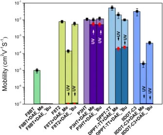
Electrical properties in OTFTs. To explore the electrical properties of the bi-component films, the polymer/DAE blends have been integrated in bottom-contact bottom-gate OTFTs, and the device mobility and photo-programmed Ion/Ioff ratio (the ratio of current in the initial state and after
UV irradiation) have been quantified, with the ultimate goal of casting light onto the charge transport properties of the chosen materials. Towards this end, OTFT assembled on SiO2/Si substrates with pre-patterned gold interdigitated
electrodes as source and drain contacts were used. The SiO2
substrates were treated with octadecyltrichlorosilane (OTS). The bi-component blends were then spin-coated (see details in SI). It is already known that the output cur- rent in P3HT/DAEs-based OTFTs can be tuned by illumina-tion at defined wavelengths. The driving mechanism is that the HOMO level of P3HT (-4.8 eV) is higher than that of DAEs in their open form (-5.6 eV), and approximately equal to the closed form (around -4.8 eV), thus the holes can be only trapped by the closed DAEs upon UV light irradiation, but not by the open-ring DAEs.5a To further investigate the optically switching function of other polymer/DAE blend-based OTFTs, we firstly summarized the HOMO levels of the polymers and DAEs in Figure 1D. Amorphous/disordered F8T2 and F8BT have HOMO levels of -5.6 eV and -5.9 eV, re-spectively. 12 It should be noted that the HOMO level of F8BT
is lower than those of the DAEs both in their open and closed form, therefore the hole transport is energetically unfavorable in the presence of DAEs. The HOMO levels of the DPPT-TT and IIDDT-C3 (-5.2 eV and -5.5 eV, respec- tively) are lying in between those of the closed and open iso-mers of DAEs. 13, 14b Figure 5. The device mobility of the neat polymers and poly- mer/DAE blends-based OTFTs (error bar in black, before irra- diation), and their UV light response (error bar in red). The mo- bility is extracted from the transfer characteristics in the satu-ration regime (Figure S6), and calculated using eq. (1) provided in the Supplementary Information. The device mobilities (extracted from the transfer char- acteristics in the saturation regime, see Supplementary In-formation for materials and characterization) of the neat polymers and polymer/DAE blends-based OTFTs are re-ported in Figure 5, and the transfer curves are plotted in Figure S6. Neat F8BT transistors showed a mobility of 1×10 -5 cm2V-1s-1. As expected, drain current was detected within the noise of the measurement after blending with DAE mol-ecules, since both the open and closed DAEs act as trap for the holes. Compared to the mobility of neat F8T2 film (8×10 -3 cm2V-1s-1), F8T2/DAE_t
Bu OTFT showed a very small de-crease in the mobility (6×10⁻³ cm2V-1s-1), whereas more
than one order of magnitude decrease was observed in F8T2/DAE_Me OTFTs (1.5×10⁻⁴ cm2V-1s-1). The reduced
mobility in the latter case is possibly due to DAE_Me mole- cules having a higher tendency to aggregate into F8T2 ma- trix thus impacting the polymer packing. The increased sur-face roughness and the similar HOMO levels of the open DAE_Me and F8T2 could easily cause the trapping and/or scattering of the hole transport. For the addition of DAEs into the matrix of P3HT a mobility in the same order of mag-nitudes as neat P3HT was observed, consistent with our previous results.5a, 5b This can be explained by the facts of: 1)
the DAE molecules reside in the amorphous region of P3HT, not strongly affecting the packing of P3HT; 2) the HOMO levels of the open DAEs is 800 meV below that of P3HT, which is not accessible for mobile holes thus minimizing the influence on charge transport in P3HT. DPPT-TT/DAE blends, with the HOMO difference of 400 meV from that of the open DAEs, also indicated the mobilities in the same or-der of magnitude as neat DPPT-TT. A small decrease in the mobility was observed when comparing the neat DPPT-TT (0.05 cm2V-1s-1) to the DPPT-TT/DAE_Me blend (0.02 cm2V -1s-1) and the DPPT-TT/DAE_tBu blend (0.01 cm2V-1s-1). The
slight change in mobility could be explained by: firstly, the smaller difference between HOMO levels compared to the case of P3HT; secondly, the fact that the crystalline struc-ture of DPPT-TT polymer matrices is mildly disrupted by DAE molecules permeation. We note that DPPT-TT/DAE blends show the highest charge mobility in all of our inves-tigated blends. In the case of IIDDT-C3, the mobility was dramatically affected when blending with DAE molecules, from 0.03 cm2V-1s-1 for neat IIDDT-C3 to 2.5×10⁻⁵ cm2V-1s-1
for IIDDT-C3/DAE_Me blend and 4.5×10⁻⁴ cm2V-1s-1 for
IIDDT-C3/DAE_t
Bu blends. The small injection barrier, con-sisting of only 100 meV from the HOMO level of the open DAEs (-5.6 eV) to that of IIDDT-C3 (-5.5 eV), provides high probability for holes scattering and/or trapping by DAE molecules and thus reducing the electrical performance. It is interesting to note that the impact of blending DAEs on the device mobility of F8T2, DPPT-TT or IIDDT-C3 is corre-lated with the roughness change evidenced by AFM imaging, i.e., the rougher the surface compared to that of neat poly- mer, the greater is the reduction in mobility. This modula-tion is magnified when the energy gap between the open DAE and polymers is becoming smaller. The films of DAE_Me blended with F8T2 and IIDDT-C3 exhibit both a
10-7 10-6 10-5 10-4 10-3 10-2 10-1 M o b lili ty ( cm 2 V -1 S -1 ) F8BT +DAE _tBu F8B T+DA E_M e F8B T F8B T+DA E_ tBu F8B T+DA E_M e F8B T UV UV F8T2 F8T2+ DAE_M e F8T2+ DAE_ tBu P3H T+DA E_ tBu P3H T+DA E_M e P3H T UV UV UV DPPT -TT+ DAE_ tBu DPPT -TT+ DAE_ Me DPPT -TT UV UV IIDDT -C3+ DAE_ tBu IIDDT -C3+ DAE_ Me IIDDT -C3 UV
7
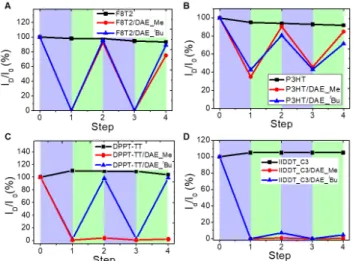
higher roughness than those of DAE_ tBu blends, and lower hole mobilities in OTFTs. Such reduced electronic charac-teristics in rougher films can be due to the more disordered packing of the guest molecules within the polymer matrix and the increased content of grain boundaries hindering ef-ficient charge transport.19 Figure 6. The reversible modulation of output current of poly- mer/DAEs-based OTFTs over irradiation cycles with UV irradi-ation (312 nm, violet shaded areas) and visible irradimer/DAEs-based OTFTs over irradiation cycles with UV irradi-ation (540 nm, green shaded areas). (A) F8T2, F8T2/DAE_Me, and F8T2/DAE_ tBu-based OTFTs at Vd=-20 V and Vd=-60 V. (B)P3HT, P3HT/DAE_Me, and P3HT/DAE_ tBu-based OTFTs at
Vd=-20 V and Vd=-60 V. (C) DPPT-TT, DPPT-TT/DAE_Me, and
DPPT-TT/DAE_ tBu based-OTFTs at Vd=-50 V and Vd=-60 V. (D)
IIDDT-C3, IIDDT-C3/DAE_Me, and IIDDT-C3/DAE_ t
Bu based-OTFTs at Vd=-20 V and Vd=-60 V. The irradiation steps were
carried out until no variation in drain current was observed upon further illumination at the same wavelength. All values are normalized to initial value before any irradiation and the connecting lines serve as ‘guides to the eye’.
A decrease in output current and device mobility in poly- mer/DAE blend-based OTFTs was observed upon UV illu-mination (Figure 5 and S7), as the consequence of hole-trapping by closed DAEs. We note that the larger the HOMO gap between the closed DAEs and polymer, the higher is the photo-programmed Ion/Ioff ratio. In the cases of F8T2 and
IIDDT-C3, with HOMO levels ~700 meV below those of the closed-form DAEs, the Ion/Ioff ratios are above 103. The
Ion/Ioff ratio of DPPT-TT/DAEs-based OTFTs was found to be
~102 upon UV irradiation. With the very similar energy
HOMO levels of the closed DAE and P3HT, the Ion/Ioff ratio
was measured at only ~10.
The reversibility of the drain current tuning of poly-mer/DAE blends-based OTFTs was investigated by per-forming two cycles of alternating irradiations at different wavelength (312 nm or 540 nm) (Figure 6). The drain cur-rent modulations of pristine polymers by light irradiation were below 10%. The variation is due to trapping of charges under bias stress and generation of mobile carriers under light irradiation. Noteworthy, no feature of reversible change was observed in neat polymers when the illuminat-ing wavelength varied. In contrast, DAE_Me and DAE_tBu
showed efficient current modulation and good reversibility in P3HT and F8T2 polymer matrices. In the latter case, the drain current is ~ 103 times less than the initial value when
the equilibrium upon UV irradiation is reached. Blending DAE_Me with highly ordered polymers (DPPT-TT and IIDDT-C3) led to an irreversible change of the drain current. A similar behavior was observed in DAE_Me and BTBT blends.5b
It can be explained by the lower photocyclorever-sion quantum yield and higher PSS of DAE_Me in DPPT-TT and IIDDT-C3 matrices (as discussion in photochemical properties). Upon visible irradiation, a very small fraction of DAE_Me in their closed form still resided in the polymer matrices, sufficient to trap the transporting holes and thus keeping the drain current at a very low level. In contrast, the steric tert-butyl substituents in DAE_tBu resulted in a
weaker association in the matrix of crystalline domain, as-sociated with slightly higher photocycloreversion quantum yield and lower PSS, compared to DAE_Me. This might ex-plain the almost full recovery of the drain current in the case of DPPT-TT and only 10% recovery in the case of IIDDT-C3 upon visible irradiation. Besides the limited propensity for photocycloreversion of the DAE, the reduction of the device performance after several switching cycles is governed by the photostability of the polymer matrix as well as intrinsic fatigue of DAE molecules, while DAE_Me and DAE_tBu show reasonable fatigue resistance in solution and in films.5b, 21 The fatigue resistance of polymer/DAE-based OTFTs over alternative light irradiation can be further improved by choosing photostable polymers and DAEs featuring high fa-tigue resistance.
DISCUSSIONs
The study of photophysical and photochemical properties of the DAE based blends revealed a strong dependence of the PSS and photochemical quantum yield of DAE on struc- ture of the polymer matrix. When embedded in highly or-dered polymer matrices, such as those based on IIDDT-C3 and DPPT-TT, the antiparallel conformation of DAEs is likely to be constrained, yielding relatively high efficiency in the process of the ring-closure and higher PSS under UV light irradiation, but lower efficiency in the process of the ring-opening of DAEs under visible light irradiation. The closed DAE features a cofacial orientation of the coplanar planes,20 which allows the molecules to easily pack in therigid inner space of highly ordered polymers. Once the closed DAEs have been restricted in the rigid environment, they are hindered to undergo back isomerization to the more flexible and space occupying open isomer. On the other hand, the flexible inner spaces in amorphous and poorly ordered polymer matrices allow the closed DAEs to undergo relatively free movement back to the open isomer, as evidenced by an over five times higher Фvis. The reduced
PSS and Фuv in F8BT, F8T2 and P3HT, compared to those of
DAEs in highly ordered polymer matrices, may result from less antiparallel conformation constrained. When com-pared to DAE_Me, the DAE_tBu inserted in highly ordered
semicrystalline polymer matrix displays a slightly lower PSS and ФUV, but higher Фvis
, indicating that when embed-ded in a polymer matrix, the constrains of the DAE_tBu is
more moderate than those of DAE_Me, because the four
tert-butyl side group determine lower tendency to self-ag-gregation and agtert-butyl side group determine lower tendency to self-ag-gregation in polymer matrices. The ring- closure is less efficient in the tert-butyl case because of ste-ric strain, and the closed isomer is less stabilized favoring ring-opening, due to a smaller thermal barrier in the excited state of photocycloreversion.
8
The photophysical and photochemical behavior of poly-mer/DAE pairs is found to correlate well with the reversible modulation of output current in optically switchable OTFTs. The free movement of DAEs in amorphous and poorly or-dered polymers enables effective photoisomerization of both ring opening and closing, and optical switching behav- ior of F8T2/DAE-based and P3HT/DAE-based OTFTs is sta-ble over several cycles (Figure 6A and 6B). As the closed DAEs act as charge traps within the matrices, the higher PSS and Фuv of DAEs
in the highly ordered DPPT-TT and IIDDT-C3 results in a significant decrease in output current upon UV irradiation (the first UV light irradiation step in Figure 6C and 6D). However, the closed DAEs is strongly hindered to undergo the photocycloreversion (Фvis
< 0.1%) in the ma-trices of DPPT-TT and IIDDT-C3 upon further visible light irradiation, thus the transported charge is still trapped by residual closed DAEs causing the non-reversible modula-tion of output current of DPPT-TT/DAE_Me-based and
IIDDT-C3/DAE_Me-based OTFTs. DAE_tBu has the
ad-vantage to more readily recover to the open isomer when compared to DAE_Me under visible light irradiation. We ob- served that output current recovery to about 10% in IIDDT-C3/DAE_tBu with a small bandgap between IIDDT-C3 and the open DAE_ tBu (100 meV), and considerable recovery in DPPT-TT/DAE_tBu with a larger bandgap (400 meV). The AFM images of bicomponent films provided evidence for the good miscibility of DAEs with the chosen polymers. Increase of the surface roughness was observed when DAEs were embedded in polymer matrices. Compared to the case of DAE_tBu, blending DAE_Me with F8T2 and IIDDT-C3
yielded rougher surfaces. The change of surface roughness resulted in variation of field-effect mobility of the polymers after introducing DAE molecules. We found that the rougher surface upon blending DAE_Me had lower mobility in F8T2 and IIDDT-C3, compared to DAE_ tBu in the same polymers.
The increase of roughness, which is an indication of a greater amount of grain boundaries as a result of the blend- ing with DAE molecules, determines a reduction in the de-vice mobility. GIWAXS revealed that the crystalline struc-ture of DPPT-TT and IIDDT-C3 polymer matrices is mildly disrupted by DAE molecules permeation, which explains the strong effect on the photoisomerization of DAEs and the decrease in device mobility in highly ordered polymers-based films. In the case of P3HT, DAE molecules reside in the amorphous regions and do not disrupt in the molecular packing of P3HT crystalline grains; as a result, the mobility of P3HT/DAE blends is comparable to that of neat P3HT films, and the photochemical processes of DAEs are similar to the case of amorphous F8T2 and F8BT. The energy levels of polymers and DAEs is another key factor that governs the performance of optically switchable OTFTs. In order to tune the output current through the op-tical control, it is required that the energy levels of applied polymers are located in between phototunable energy lev-els of DAEs. As a counter example of F8BT, whose HOMO energy level is lying even lower than that of chosen DAEs in their open forms, blending these two components induces direct trapping of the holes, thus no hole conduction could be observed. The position of HOMO levels of the polymers, closer to that of the open DAEs or the closed DAEs, strongly influences both mobility and photo-programmed Ion/Ioff
ra-tio. When the HOMO of the polymers is far above that of the
open DAEs, as is the case for P3HT and DPPT-TT, the mobil-ity of the blends remains as high as the pristine polymers. The large energy gap, 800 meV for P3HT and 400 meV for DPPT-TT, leads to the open DAE molecules not accessible for mobile holes thus minimize the influence of charge transport. The smaller bandgap between embedded poly-mers and the ring-open DAEs, together with the increased roughness, lead to stronger charge scattering and the possi-bility of trapping by the open DAEs in the polymer matrix, thus to some extent reduce the mobility of polymers, as was observed in the cases of F8T2/DAE_Me and IIDDT-C3/DAE_Me blends. However, if the HOMO of the polymers is much lower than that of the closed DAE, the UV light irra-diation can result in an increased photo-programmable Ion/Ioff ratio, surpassing 1000 in the case of F8T2/DAE pairs,
due to the deep trapping. IIDDT-C3/DAE blends also exhib-ited high photo-programmed Ion/Ioff with a similar bandgap
as F8T2, however, they showed non-reversible light modu-lation due to the inefficient photocycloreversion. P3HT with the HOMO level adjacent to the closed DAE has a photo-pro-grammable Ion/Ioff
ratio about 10 because of the more mod-erate trapping.
CONCLUSION
The incorporation of photochromic diarylethenes in matri-ces of polymer semiconductors represents a powerful methodology to extend the functions of organic electronic devices with the response to external light. Here, we have reported an in-depth investigation on the performances of diarylethenes blended with organic semiconducting poly-mers featuring various microstructures and energy levels. A correlation between photoswitching, morphology, energy levels and OTFT performance of polymer/DAE blends have been thoroughly investigated. Based on our results, we have defined some important guidelines for the fabrication of high-performance optically switching organic devices: 1) photochromic molecules expected to weakly interact with the polymer matrices should be chosen to attain efficient photoisomerization quantum yields in both directions; 2) because of the amorphous nature of DAEs, polymers with lower degrees of crystallinity are better candidates, to guar-antee better mixing with DAE molecules and less influence on the packing of polymer chains; 3) if a higher device mo- bility is required, in principle, the HOMO level of the poly-mer should be close to that of the closed DAE, while if the higher photo-programmable Ion/Ioff ratio is required, the
HOMO level of the polymer should be close to that of the open DAE. In compliance with the above guidelines, we have observed optical switchable OTFTs based on F8T2/DAE_t
Bu outperforms all other combinations regard-ing rather high hole mobility (6×10⁻³ cm2V-1s-1) and high
photo-programmed Ion/Ioff ratio (>103), and
DPPT-TT/DAE_tBu based OTFT features highest hole mobility
(0.01 cm2V-1s-1)) yet accompanied by a moderate
photo-programmed Ion/Ioff ratio (102). In principle, this approach
can be applied to n-type polymer/DAE-based photoswitch-able field-effect transistors, in which the electron transport can be modulated thanks to the photoactivated switching of DAEs with one isomer acting as an electron accepting level within the n-type semiconducting polymer matrix. We are convinced that the general component-structure-perfor-mance correlation deduced from this study will guide future
9
rational design of molecularphotoswitches/semiconduct- ing polymers blends based high-performance light-respon-sive multifunctional optoelectronic devices for information storage and telecommunications. ASSOCIATED CONTENT Supporting Information. Details on materials; light irradia-tion; devices fabrication; devices characterization; UV/visible absorption; GIWAXS; transfer curves were described in sup-porting information. This material is available free of charge via the Internet at http://pubs.acs.org. AUTHOR INFORMATION Corresponding Authors * samori@unistra.fr, emanuele.orgiu@emt.inrs.ca Notes
The authors declare no competing financial interest. Present Addresses
#
Department of Chemistry and Chemical Engineering, Chalmers University of Technology, Kemigården 4, SE-412 96, Gothenburg, Sweden.
Funding Sources
This work was financially supported by the European Commis-sion through the Marie Sklodowska-Curie ITN projects iSwitch (GA-642196) and BORGES (GA-813863), the ERC projects SUPRAFUNCTION 257305) and LIGHT4FUNCTION (GA-308117), the Agence Nationale de la Recherche through the Labex project CSC (ANR-10-LABX-0026 CSC) within the Inves-tissement d’Avenir program (ANR-10-120 IDEX-0002-02), and the International Center for Frontier Research in Chemistry (icFRC) as well as the German Research Foundation (via SFB 951). E. O. is supported by the Natural Sciences and Engineer-ing Research Council of Canada (NSERC) through an individual Discovery Grant.
REFERENCES
(1) (a) Feringa, B. L., The art of building small: From molecular switches to molecular motors. J. Org. Chem.
2007, 72 (18), 6635-6652. (b) Hou, L. L.; Zhang, X. Y.;
Pijper, T. C.; Browne, W. R.; Feringa, B. L., Reversible Photochemical Control of Singlet Oxygen Generation Using Diarylethene Photochromic Switches. J. Am. Chem. Soc.
2014, 136 (3), 910-913. (c) Mativetsky, J. M.; Pace, G.;
Elbing, M.; Rampi, M. A.; Mayor, M.; Samorì, P., Azobenzenes as light-controlled molecular electronic switches in nanoscale metal-molecule-metal junctions. J.
Am. Chem. Soc. 2008, 130 (29), 9192-9193. (d)
Szymanski, W.; Beierle, J. M.; Kistemaker, H. A. V.; Velema, W. A.; Feringa, B. L., Reversible Photocontrol of Biological Systems by the Incorporation of Molecular Photoswitches. Chem. Rev. 2013, 113 (8), 6114-6178. (e) Wang, J. B.; Hou, L. L.; Browne, W. R.; Feringa, B. L., Photoswitchable Intramolecular Through-Space Magnetic Interaction. J. Am. Chem. Soc. 2011, 133 (21), 8162-8164. (2) (a) Irie, M.; Fukaminato, T.; Matsuda, K.; Kobatake, S., Photochromism of Diarylethene Molecules and Crystals: Memories, Switches, and Actuators. Chem. Rev. 2014, 114 (24), 12174-12277. (b) Tian, H.; Yang, S. J., Recent progresses on diarylethene based photochromic switches.
Chem. Soc. Rev. 2004, 33 (2), 85-97.
(3) (a) Dimitrakopoulos, C. D.; Malenfant, P. R. L., Organic thin film transistors for large area electronics. Adv. Mater.
2002, 14 (2), 99-117. (b) Dimitrakopoulos, C. D.; Mascaro,
D. J., Organic thin-film transistors: A review of recent
advances. Ibm J. Res. Dev. 2001, 45 (1), 11-27. (c) Forrest, S. R.; Thompson, M. E., Introduction: Organic electronics and optoelectronics. Chem. Rev. 2007, 107 (4), 923-925. (d) Sondergaard, R. R.; Hosel, M.; Krebs, F. C., Roll-to-Roll fabrication of large area functional organic materials. J. Polym. Sci. Pol. Phys. 2013, 51 (1), 16-34. (4) (a) Orgiu, E.; Samorì, P., 25th Anniversary Article: Organic Electronics Marries Photochromism: Generation of Multifunctional Interfaces, Materials, and Devices. Adv.
Mater. 2014, 26 (12), 1827-1845. (b) Zhang, X. Y.; Hou,
L. L.; Samorì, P., Coupling carbon nanomaterials with photochromic molecules for the generation of optically responsive materials. Nat. Commun. 2016, 7. 11118. (c) Goulet-Hanssens, A.; Eisenreich, F.; Hecht, S., Enlightening materials with photoswitches. Adv. Mater. 2020, 1905966 (d) Jia, C. C.; Migliore, A.; Xin, N.; Huang, S. Y.; Wang, J. Y.; Yang, Q.; Wang, S. P.; Chen, H. L.; Wang, D. M.; Feng, B. Y.; Liu, Z. R.; Zhang, G. Y.; Qu, D. H.; Tian, H.; Ratner, M. A.; Xu, H. Q.; Nitzan, A.; Guo, X. F., Covalently bonded single-molecule junctions with stable and reversible photoswitched conductivity. Science 2016, 352 (6292), 1443-1445. (e) Hou, L. L.; Zhang, X. Y.; Cotella, G. F.; Carnicella, G.; Herder, M.; Schmidt, B. M.; Patzel, M.; Hecht, S.; Cacialli, F.; Samorì, P., Optically switchable organic light-emitting transistors. Nat. Nanotechnol. 2019,
14 (4), 347-353. (f) Zacharias, P.; Cather, M. C.; Köhnen,
A.; Rehmann, N.; Meerholz, K., Photosprogrammable organic light-emitting diodes. Angew. Chem. Int. Ed. 2009,
48, 4038-4041.
(5) (a) Orgiu, E.; Crivillers, N.; Herder, M.; Grubert, L.; Patzel, M.; Frisch, J.; Pavlica, E.; Duong, D. T.; Bratina, G.; Salleo, A.; Koch, N.; Hecht, S.; Samorì, P., Optically switchable transistor via energy-level phototuning in a bicomponent organic semiconductor. Nat. Chem. 2012, 4 (8), 675-679. (b) El Gemayel, M.; Borjesson, K.; Herder, M.; Duong, D. T.; Hutchison, J. A.; Ruzie, C.; Schweicher, G.; Salleo, A.; Geerts, Y.; Hecht, S.; Orgiu, E.; Samorì, P., Optically switchable transistors by simple incorporation of photochromic systems into small-molecule semiconducting matrices. Nat Commun 2015, 6. 6330. (c) Borjesson, K.; Herder, M.; Grubert, L.; Duong, D. T.; Salleo, A.; Hecht, S.; Orgiu, E.; Samorì, P., Optically switchable transistors comprising a hybrid photochromic molecule/n-type organic active layer. J. Mater. Chem. C 2015, 3 (16), 4156-4161. (6) Leydecker, T.; Herder, M.; Pavlica, E.; Bratina, G.; Hecht, S.; Orgiu, E.; Samorì, P., Flexible non-volatile optical memory thin-film transistor device with over 256 distinct levels based on an organic bicomponent blend. Nat.
Nanotechnol. 2016, 11 (9), 769-775.
(7) (a) Gwinner, M. C.; Khodabakhsh, S.; Song, M. H.; Schweizer, H.; Giessen, H.; Sirringhaus, H., Integration of a Rib Waveguide Distributed Feedback Structure into a Light-Emitting Polymer Field-Effect Transistor. Adv .Funct.
Mater. 2009, 19 (11), 1686-1686. (b) Gwinner, M. C.;
Vaynzof, Y.; Banger, K. K.; Ho, P. K. H.; Friend, R. H.; Sirringhaus, H., Solution-Processed Zinc Oxide as High-Performance Air-Stable Electron Injector in Organic Ambipolar Light-Emitting Field-Effect Transistors. Adv.
Funct. Mater. 2010, 20 (20), 3457-3465.
(8) Deng, Y. Y.; Sirringhaus, H., Optical absorptions of polyfluorene transistors. Phys. Rev. B. 2005, 72 (4), 045207.
(9) (a) Noh, Y. Y.; Sirringhaus, H., Ultra-thin polymer gate dielectrics for top-gate polymer field-effect transistors. Org.
Electron. 2009, 10 (1), 174-180. (b) Salleo, A., Charge
transport in polymeric transistors. Mater. Today 2007, 10 (3), 38-45.
(10) (a) Chen, Z. Y.; Lee, M. J.; Ashraf, R. S.; Gu, Y.; Albert-Seifried, S.; Nielsen, M. M.; Schroeder, B.; Anthopoulos, T. D.; Heeney, M.; McCulloch, I.; Sirringhaus, H., High-Performance Ambipolar Diketopyrrolopyrrole-Thieno[3,2-b]thiophene Copolymer Field-Effect Transistors with
10
Balanced Hole and Electron Mobilities. Adv Mater 2012, 24 (5), 647-652. (b) Li, W. W.; Hendriks, K. H.; Roelofs, W. S. C.; Kim, Y.; Wienk, M. M.; Janssen, R. A. J., Efficient Small Bandgap Polymer Solar Cells with High Fill Factors for 300 nm Thick Films. Adv. Mater. 2013, 25 (23), 3182-3186. (c) Zhang, X. R.; Richter, L. J.; DeLongchamp, D. M.; Kline, R. J.; Hammond, M. R.; McCulloch, I.; Heeney, M.; Ashraf, R. S.; Smith, J. N.; Anthopoulos, T. D.; Schroeder, B.; Geerts, Y. H.; Fischer, D. A.; Toney, M. F., Molecular Packing of High-Mobility Diketo Pyrrolo-Pyrrole Polymer Semiconductors with Branched Alkyl Side Chains. J. Am.
Chem. Soc. 2011, 133 (38), 15073-15084. (d) Li, Y. N.;
Sonar, P.; Singh, S. P.; Soh, M. S.; van Meurs, M.; Tan, J., Annealing-Free High-Mobility Diketopyrrolopyrrole-Quaterthiophene Copolymer for Solution-Processed Organic Thin Film Transistors. J. Am. Chem. Soc. 2011, 133 (7), 2198-2204.
(11) (a) Lei, T.; Cao, Y.; Fan, Y. L.; Liu, C. J.; Yuan, S. C.; Pei, J., High-Performance Air-Stable Organic Field-Effect Transistors: Isoindigo-Based Conjugated Polymers. J. Am.
Chem. Soc. 2011, 133 (16), 6099-6101. (b) Lei, T.; Dou,
J. H.; Pei, J., Influence of Alkyl Chain Branching Positions on the Hole Mobilities of Polymer Thin-Film Transistors. Adv.
Mater. 2012, 24 (48), 6457-6461.
(12) (a) Zaumseil, J.; Donley, C. L.; Kim, J. S.; Friend, R. H.; Sirringhaus, H., Efficient top-gate, ambipolar, light-emitting field-effect transistors based on a green-light-emitting polyfluorene. Adv. Mater. 2006, 18 (20), 2708-2712. (b) Ravirajan, P.; Haque, S. A.; Durrant, J. R.; Poplavskyy, D.; Bradley, D. D. C.; Nelson, J., Hybrid nanocrystalline TiO2 solar cells with a fluorene-thiophene copolymer as a sensitizer and hole conductor. J. Appl. Phys.
2004, 95 (3), 1473-1480.
(13) (a) Fukaminato, T.; Umemoto, T.; Iwata, Y.; Yokojima, S.; Yoneyama, M.; Nakamura, S.; Irie, M., Photochromism of diarylethene single molecules in polymer matrices. J. Am.
Chem. Soc. 2007, 129 (18), 5932-5938. (b) Ikeda, M.;
Tanifuji, N.; Yamaguchi, H.; Irie, M.; Matsuda, K., Photoswitching of conductance of diarylethene-Au nanoparticle network. Chem. Commun. 2007, 13, 1355-1357.
(14) (a) Santos, A. R.; Ballardini, R.; Belser, P.; Gandolfi, M. T.; Iyer, V. M.; Moggi, L., Photochemical investigation of a photochromic diarylethene compound that can be used as a wide range actinometer. Photoch. Photobio. Sci. 2009, 8 (12), 1734-1742. (b) Sumi, T.; Takagi, Y.; Yagi, A.; Morimoto, M.; Irie, M., Photoirradiation wavelength dependence of cycloreversion quantum yields of diarylethenes. Chem. Commun. 2014, 50 (30), 3928-3930. (15) (a) Noriega, R.; Rivnay, J.; Vandewal, K.; Koch, F. P. V.; Stingelin, N.; Smith, P.; Toney, M. F.; Salleo, A., A general relationship between disorder, aggregation and charge transport in conjugated polymers. Nat. Mater. 2013,
12 (11), 1038-1044. (b) Salleo, A.; Kline, R. J.;
DeLongchamp, D. M.; Chabinyc, M. L., Microstructural Characterization and Charge Transport in Thin Films of Conjugated Polymers. Adv. Mater. 2010, 22 (34), 3812-3838. (c) Qian, Z.; Cao, Z.; Galuska, L.; Zhang, S.; Xu, J.; Gu, X., Glass Transition Phenomenon for Conjugated Polymers. Macromol. Chem. Phys. 2019, 220, 1900062. (16) (a) Cheng, X. Y.; Noh, Y. Y.; Wang, J. P.; Tello, M.; Frisch, J.; Blum, R. P.; Vollmer, A.; Rabe, J. P.; Koch, N.; Sirringhaus, H., Controlling Electron and Hole Charge Injection in Ambipolar Organic Field-Effect Transistors by Self-Assembled Monolayers. Adv. Funct. Mater. 2009, 19 (15), 2407-2415. (b) Kline, R. J.; McGehee, M. D.; Kadnikova, E. N.; Liu, J. S.; Fréchet, J. M. J., Controlling the field-effect mobility of regioregular polythiophene by changing the molecular weight. Adv. Mater. 2003, 15 (18), 1519-1522.
(17) (a) Kettner, O.; Pein, A.; Trimmel, G.; Christian, P.; Rothel, C.; Salzmann, I.; Resel, R.; Lakhwani, G.; Lombeck,
F.; Sommer, M.; Friedel, B., Mixed side-chain geometries for aggregation control of poly(fluorene-alt-bithiophene) and their effects on photophysics and charge transport.
Synthetic Met. 2016, 220, 162-173. (b) Yang, Y.; da Costa,
R. C.; Smilgies, D. M.; Campbell, A. J.; Fuchter, M. J., Induction of Circularly Polarized Electroluminescence from an Achiral Light-Emitting Polymer via a Chiral Small-Molecule Dopant. Adv. Mater. 2013, 25 (18), 2624-2628. (18) Giri, G.; Verploegen, E.; Mannsfeld, S. C. B.; Atahan-Evrenk, S.; Kim, D. H.; Lee, S. Y.; Becerril, H. A.; Aspuru-Guzik, A.; Toney, M. F.; Bao, Z. A., Tuning charge transport in solution-sheared organic semiconductors using lattice strain. Nature 2011, 480 (7378), 504-U124.
(19) Jung, Y.; Kline, R. J.; Fischer, D. A.; Lin, E. K.; Heeney, M.; McCulloch, I.; DeLongchamp, D. M., The effect of interfacial roughness on the thin film morphology and charge transport of high-performance polythiophenes. Adv.
Funct. Mater. 2008, 18 (5), 742-750.
(20) Irie, M.; Kobatake, S.; Horichi, M., Reversible surface morphology changes of a photochromic diarylethene single crystal by photoirradiation. Science 2001, 291 (5509), 1769-1772.
(21) Herder, M.;Schmidt, B. M.; Grubert, L.; Pätzel, M.; Schwarz, J.; Hecht, S., Improving the Fatigue Resistance of Diarylethene Switches. J. Am. Chem. Soc. 2015, 137, 2738-2747.