Viatcheslav Vertlib
Laboratory for Clay Mineralogy, Institute for Geotechnical Engineering, ETH Zurich, 8093 Zurich, Switzerland
Marianne Dietiker
Laboratory for Nanometallurgy, Department of Materials, ETH Zurich, 8093 Zurich, Switzerland
Michael Plötzea)and Lee Yezek
Laboratory for Clay Mineralogy, Institute for Geotechnical Engineering, ETH Zurich, 8093 Zurich, Switzerland
Ralph Spolenak
Laboratory for Nanometallurgy, Department of Materials, ETH Zurich, 8093 Zurich, Switzerland
Alexander M. Puzrin
Laboratory for Clay Mineralogy, Institute for Geotechnical Engineering, ETH Zurich, 8093 Zurich, Switzerland
(Received 30 October 2007; accepted 17 January 2008)
This paper presents a spin-coating layer-by-layer assembly process to prepare multilayered polyelectrolyte-clay nanocomposites. This method allows for the fast production of films with controlled layered structure. The preparation of a 100-bilayer film with a thickness of about 330 nm needs less than 1 h, which is 20 times faster than conventional dip-coating processes maintaining the same hardness and modulus values. For validation of this technique, nanocomposite films with thicknesses up to 0.5m have been created with the common dip self-assembly and with the spin coating layer-by-layer assembly technique from a poly(diallyldimethylammonium)chloride (PDDA) solution and a suspension of a smectite clay mineral (Laponite). Geometrical characteristics (thickness, roughness, and texture) as well as mechanical characteristics (hardness and modulus) of the clay-polyelectrolyte films have been studied. The spin-coated nanocomposite films exhibit clearly improved mechanical properties (hardness 0.4 GPa, elastic modulus 7 GPa) compared to the “pure” polymer film, namely a sixfold increase in hardness and a 17-fold increase in Young’s modulus.
I. INTRODUCTION
Multilayered polymer-clay nanocomposites have at-tracted considerable attention due to their mechanical properties, which resemble those of naturally occurring composite materials with layered brick-and-mortar struc-ture, such as nacre.1,2 The composite materials are con-stituted of hard components (e.g., silica particles, fibers, carbonates, and clay platelets) and soft material (e.g., positively charged polymers); each brings into the sys-tem its particular qualities. While the hard phase (the “brick”) provides stiffness and mechanical stability to the system, the function of the matrix (the “mortar”) is to maintain the geometry of the structure and to distribute the mechanical stresses among the hard constituents, pro-viding at the same time high fracture toughness and
im-proving the fatigue resistance. Several toughening mechanisms like crack blunting, branching and deflec-tion, platelet pullout, crack bridging, and sliding of plate-let sublayers allow higher energy consumption.3–5
Different layer-by-layer (LBL) assembly techniques, based on sequential adsorption of oppositely charged compounds, have been established for preparation of multilayered thin films. The driving force for the adsorp-tion of the components, which is carried out from dilute aqueous solution, is electrostatic. Currently, the most commonly used method for preparing multilayered poly-electrolyte-clay nanocomposite films is based on a dip self-assembly process.6–8This LBL assembly simply in-volves dipping a substrate into dilute aqueous solution, so that it is relatively easy to control the number, type, and sequence of layers added to the film, even on non-planar surfaces. However, this method possesses a seri-ous disadvantage of being extremely time consuming. In an alternative dripping self-assembly method, the solu-tions were sequentially dripped on the film surface and,
a)
Address all correspondence to this author. e-mail: [email protected] DOI: 10.1557/JMR.2008.0147
after some seconds, rinsed with water and blown dry with nitrogen.7In addition, there are production routes using, e.g., directional freezing of aqueous solutions with sub-sequent ice sublimation,9progressive evaporation of dis-persions with low concentrations of delaminated plate-lets,10
or evaporation-induced self-assembly.11
The evap-oration-induced film production is a well-established method for preparing textured specimens in x-ray dif-fraction (XRD) clay mineralogical analysis.12,13
The ad-vantages are the simple building process and the possi-bility for preparing large and thick films with high or-dering of the crystallites in the z direction. A drawback is the crack formation during drying. A further possibility for preparing composite films is the spin self-assembly method.14,15 In contrast to those mentioned above, this method allows the rapid production of films with con-trolled layered structure and extremely low surface roughness on planar substrates.
The aim of this research was to explore the fast spin-self-assembly approach for the preparation of polymer-clay nanocomposite films and, using nanoindentation, to compare the mechanical properties of nanocomposite films prepared by spin and dip self-assembly processes.
II. EXPERIMENTAL
Poly(diallyldimethylammonium)chloride (PDDA) (Sigma-Aldrich, Buchs, Switzerland) was used in the form of 20 wt% water solution (low molecular weight, Mw ⳱ 100,000 to 200,000) without purification. The solutions for film assembling were prepared by further dilution of this 20 wt% batch solution with water. Water was purified by a Millipore (Zug, Switzerland) Milli-Q Gradient system. Laponite was supplied by Laporte In-dustries (Widnes, UK). Laponite is entirely synthetic trioctahedral Na+-smectite similar to natural hectorite. The Laponite platelets have a disklike shape with an aspect ratio (w/t) of 25.
The permanent negative surface charge gives a cation exchange capacity (CEC) of 75 meq/100 g clay. The Laponite suspensions were freshly prepared by disper-sion in purified water and stirring for 2 h.
The standard 6-in. 〈100〉 silicon wafers as substrates were cut in 18-mm-diameter disks or 30 mm × 20 mm rectangles. The wafer surfaces were ultrasonically cleaned in 50% aqueous ethanol and afterwards oxidized with hot (∼100 °C) mixture (1:1 by volume) of 98% sul-furic acid and 30% hydrogen peroxide (piranha). The thickness of the formed SiO2layer on the oxidized sili-con substrate was found, using ellipsometry, to be be-tween 2 and 3 nm.
The dip self-assembly has been performed using a PC-operated Nima DC-multi dip coater with 16 dipping ves-sels (Nima Technology Ltd., Coventry, UK). A flat rect-angular substrate was sequentially dipped in PDDA
so-lution and clay suspension.16–20The dip cycle program for each bilayer consisted of six steps: dipping into PDDA (0.05 wt%, pH 5.7) solution for 300 s, rinsing three times with water, dipping in Laponite (0.05 wt%, pH 9.7) sus-pension for 300 s, and finally rinsing two times with water. The preparation of a 100-bilayer film takes about 17 h.
The spin self-assembly process of multilayer forma-tion consisted of four continuous steps: some drops of the cationic polymer solution on the silicon disk until full coverage, spinning at 60 rps for about 30 s until dry, spin washing with purified water, dropping the clay suspen-sion on the polymer surface until full coverage, spinning at 60 rps for about 30 s, and spin washing with purified water. A spin coater SCI-50 (LOT-Oriel, Darmstadt, Germany) was used. In less than 2 h a 100-bilayer film can be produced.
The geometrical characteristics of the prepared films such as thickness, roughness, and inner structure were studied with ellipsometry measurements, XRD, thermo-gravimetric analysis (TGA), and microscopic methods. The variable angle spectroscopic ellipsometry (VASE) spectra were measured under ambient conditions in tem-perature and relative humidity (40%–50%) at 65°, 70°, and 75° and at wavelengths from 370 to 1000 nm (M-2000D, J.A. Woollam Co., Inc., Lincoln, NE). The VASE spectra were fitted with the multilayer model based on the WVASE32 analysis software, using the op-tical properties of a generalized Cauchy polymer (An⳱ 1.625, Bn⳱ 0, and Cn⳱ 0) and clay (An⳱ 1.57, Bn⳱ 0, and Cn⳱ 0) layers. Atomic force microscope (AFM) images were acquired with a WITec instrument (CRAFM 200, WITec GmbH, Ulm, Germany) in contact mode using silicon nitride tips. As a measure of rough-ness the standard deviation (Stdev) of the topography was calculated using WITec software. Typically, 10m × 10 m scans were acquired for this purpose under ambient conditions in temperature and relative humidity (40%– 50%). XRD patterns were recorded on a PHILIPS PW1820 diffractometer (PANalytical, Almelo, The Netherlands) with Cu K␣radiation ( ⳱ 0.154 nm) with automatic divergence slit and a secondary graphite monochromator. The scan step was 0.02° 2 with a counting time of 100 s/step. The evaluation of the pattern was carried out using DiffracPlus evaluation software (Bruker AXS, Karlsruhe, Germany). An X’Pert PW3070 x-ray diffractometer with Eulerian cradle (PANalytical, The Netherlands) was used to measure the texture of the clay platelets in the assembled films. The scan of the (001) basal reflection at 6.2° 2 with Cu K␣was carried out between 0° and 360° in steps of 5° with angles between 0° and 60° in steps of 1°. The evaluation was done with the X’Pert Texture program (PANalytical). Loading of inorganic material was characterized with TGA measuring the mass loss of Laponite only, as well as of composite material in the temperature range
between 30 and 1000 °C in dry air flow using a thermo-balance (SDTA851e, Mettler Toledo, Greifensee, Swit-zerland). Scanning electron microscopic studies were carried out using a field emission gun Leo 1530 with Gemini optics and an InLens backscattered electrons (BSE) detector (Zeiss/Leo, Oberkochen, Germany). Cross-section samples were prepared by freezing films on substrates in Nliqand subsequently breaking in pieces followed by Pt coating of the surface.
The mechanical properties of the films were charac-terized with nanoindentation using a TriboIndenter (Hysitron, Inc., Minneapolis, MN) under ambient condi-tions in temperature and relative humidity (40%–50%) with a cube corner tip. The measurements were carried out in displacement-controlled mode with a constant loading and unloading rate of 15 nm/s to depths ranging from 50 to 500 nm for the composite films and from 50 to 350 nm for the PDDA film. The effects of creep were studied for the spin-coated film by adding a hold time (1 s) at constant indentation depth between the loading and the unloading segment. On each sample, 70–100 indents were made (10 indents per indentation depth, separated by at least 30m). The drift rate was checked prior to each indentation by keeping the indenter tip at constant force (0.5N) in contact with the film surface and moni-toring the displacement for 30 s. Subsequently, the in-dentation depths were corrected for the previously deter-mined drift. Hardness H and reduced modulus Er were determined using the method of Oliver and Pharr.21 It should be noted that the reduced modulus Er, as well as the Hardness H, is a combination of the properties of both thin film and substrate. To extract “true” elastic film properties from nanoindentation experiments, Doerner and Nix22
developed a model accounting for the influ-ence of the substrate. This model was modified by King23who made it applicable to all film/substrate sys-tems using flat-ended cylindrical, quadrilateral, or trian-gular punches for indentation. To extend King’s model to three-face pyramidal tips, it was modified by Saha and Nix24and is defined as
1 Er =1− i 2 Ei +1− f 2 Ef
冉
1− e −␣共t−h兲 a冊
+1− s 2 Es冉
e −␣共t−h兲 a冊
, (1)whereiand Ei,fand Ef, andsand Esare the Poisson’s ratio and elastic modulus of diamond indenter tip, film, and substrate, respectively, a is the square root of the projected contact area A, h is the indenter displacement, t is the film thickness, and␣ is a numerically determined scaling parameter that is a function of a/t, the normalized punch size and the tip geometry. Saha and Nix24 fitted King’s numerically determined values for ␣, obtaining the following equation:
␣ = −0.37828 − 0.0056092 a t + 0.34744 a1Ⲑ2 t + 1.197a 1Ⲑ4 t . (2)
Table I shows the properties of the indenter, the sub-strate, and the films, which were used for the calculation of Ef according to Eq. (1). Thicknesses t of the PDDA and the composite films were assumed to be 400 and 470 nm, respectively. ␣ was calculated for each inden-tation depth according to Eq. (2).
III. RESULTS
A. Geometrical characteristics
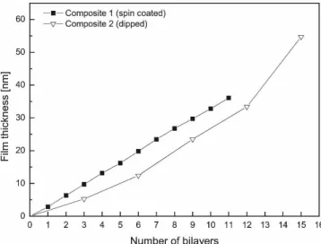
The film thickness evolution up to 11 bilayers was studied using ellipsometry. Thickness measurements of thicker films were not possible because the intensity of reflected light became too weak. The thickness of the first polymer layer deposited on the SiO2 layer of the silicon substrate was always lower than the thickness of upcoming polymer sublayers. This might have been due to the lower charge of the bare silicon dioxide surface.
FIG. 1. Film thickness evolution from the ellipsometry data. Films were prepared with 0.05 wt% PDDA solution and 0.05 wt% Laponite suspension. The average thickness of clay/polymer bilayer formed by spin self-assembly is 3.18 nm (polymer sublayer 1.06 nm, clay sub-layer 2.12 nm).
TABLE I. Assumed Poisson’s ratio and modulus of the diamond in-denter tip and the silicon substrate and assumed Poisson’s ratio of the PDDA, the spin-coated and the dipped composite film.
i Ei(GPa) s Es(GPa) f Composite f PDDA
0.0725 114125 0.2826 176a 0.25b 0.3525 aMeasured by nanoindentation.
bEstimated from the Poisson’s ratio of montmorillonite ⳱ 0.2027(2/3
The average thickness of clay/polymer bilayer formed by spin self-assembly with 0.05 wt% PDDA solution and 0.05 wt% Laponite suspension was 3.18 nm. The average polymer sublayer thickness was 1.06 nm, while the clay sublayer thickness was 2.12 nm. The thickness increase versus number of bilayers plot is almost linear for 0.05 wt% PDDA/0.05 wt% Laponite concentration (Fig. 1). Increasing of the Laponite concentration by two times had almost no effect on the average thickness of bilayer (3.28 nm). The multilayer build-up of films prepared with the dip coater and the same 0.05 wt% PDDA solution and 0.05 wt% Laponite suspension shows slightly lower film thicknesses at the early stages of film formation and not the same linear film thickness evolution as the spin-coated sample. The high surface roughness and lower optical uniformity of films pro-duced with higher PDDA concentrations (0.5 wt%), even at the early stage of formation (Table II) make well re-producible ellipsometry measurements impossible.
The thicknesses of spin self-assembly films (0.05 wt% PDDA/ 0.05 wt% Laponite) measured from the AFM scan profile of fine scratches as the difference between the average top and the average bottom topographical
level were 150 ± 20 nm for the film with 50 bilayers, 330 ± 20 nm for the film with 100 bilayers, and 460 ± 30 nm for the film with 150 bilayers. The film bilayer thickness measured by ellipsometry is consistent with AFM profilometry data (3.2 nm for one bilayer from ellipsometry versus 330 nm for 100 bilayer from AFM). The typical AFM image of the scratch is given on the Fig. 2.
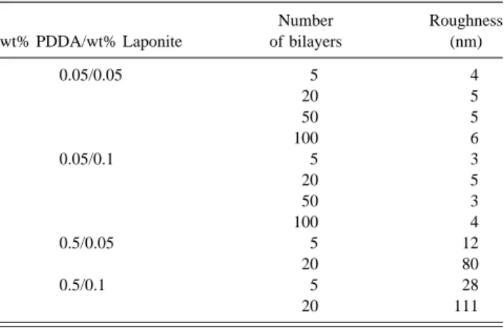
Series of films with 5, 20, 50, and 100 bilayers using a set of different PDDA and Laponite solution concen-trations were prepared to study the surface roughness evolution by AFM (Table II). To compare the properties of the composite films with one of PDDA, only a pure PDDA film was prepared by one-time spin coating of 3 wt% PDDA water solution on the silicon substrate. The PDDA film was rough and nonuniform in thickness. An average thickness of 300 ± 100 nm was determined by AFM profilometry and nanoindentation.
It was found that breaks in the continuous film-formation process up to 24 h had no effect on the film quality. However, the PDDA solution concentration was discovered to have a very strong influence on the film
FIG. 2. AFM image of a scratch in a 0.05 wt%PDDA/0.05 wt% Lapo-nite film with 100 bilayers prepared with spin self-assembly. The film thickness is 330 ± 20 nm.
FIG. 3. (a) AFM image of 100 bilayer films prepared by dip coating and (b) spin coating using 0.05 wt% PDDA solution and 0.05 wt% Laponite suspension showing the higher surface roughness of the dip self-assembly films.
TABLE II. Roughness evolution during multilayer film build-up by spin self-assembly. wt% PDDA/wt% Laponite Number of bilayers Roughness (nm) 0.05/0.05 5 4 20 5 50 5 100 6 0.05/0.1 5 3 20 5 50 3 100 4 0.5/0.05 5 12 20 80 0.5/0.1 5 28 20 111
surface roughness. Using 0.05 wt% PDDA solution and up to 0.1 wt% Laponite solution, the surface roughness for 100 bilayer films was similar to that of 5 bilayer films, whereas 0.5 wt% PDDA solution resulted in the formation of very rough films, even at an early stage of formation. A high PDDA concentration (0.5 wt%) also leads to peel off and cracking during the spin-on process. The surface roughness of films prepared with the dipping method using the same concentrations is much higher as it can be seen in the typical AFM images of 100 bilayer films on Fig. 3. In the AFM image of the dipped film, some thick stacks of clay platelets can be seen, which are caused by reaggregation during dipping in the aqueous dispersion. In contrast, the surface of the spinned film is much smoother and homogeneous.
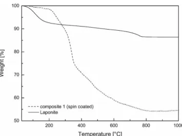
TGA analysis showed high loading of the inorganic material (Fig. 4). Up to 220 °C, the mass loss is caused by the release of surface and clay mineral interlayer ad-sorbed water, while above approximately 500 °C, it is caused by laponite dehydroxylation, which is 5%, as in the ideal case. The composite shows a mass loss of about
45%. Taking into account the mass loss from laponite dehydroxylation, a loading of inorganic material of ap-proximately 60 wt% can be revealed.
In the cross-section scanning electron microscopy (SEM) images of films prepared by spin self-assembly, the lamellar but wavy film structure can be clearly seen (Fig. 5). The observed film thickness is consistent with the AFM profilometry data (compare with Fig. 2). The dense coverage of the film surface with the Laponite particles can be observed in the SEM top view (Fig. 5). The XRD patterns of two Laponite/PDDA films pre-pared by spin and dip self-assembly are plotted on Fig. 6. Only a rational series of peaks from basal reflections can be observed, which is indicative of clay particle ordering in the z direction and a lamellar film structure. The basal distance of the Laponite increased from 12.3 Å in the original Na-form to 14.3 Å.
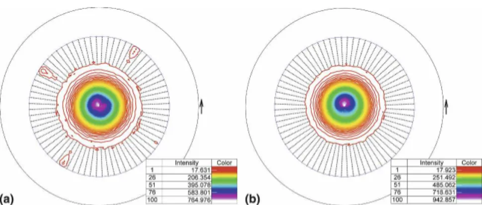
For assessment of the clay platelet orientation during film preparation, the deviation* of the tilt angles of the clay platelets around the mean crystallite orientation (z direction perpendicular to the film) were measured on the same films (Fig. 7). Zones of isointensity rings in the pole figure are indicative for the random distribution of
FIG. 4. TGA comparison of pure Laponite and spin coating composite (150 bilayer from 0.05 wt% PDDA solution and 0.05 wt% Laponite suspension).
FIG. 6. XRD patterns of multilayer films (100 bilayers for spin-coated and 135 bilayers for dipped) using 0.05 wt% PDDA solution and 0.05 wt% Laponite suspension.
FIG. 5. SEM images of a spin-coated film (150 bilayers) using 0.05 wt% PDDA solution and 0.05 wt% Laponite suspension. (a) Fractured cross section and (b) top view.
the crystallite a and b axes in the film plane for the spin-coated film. The dipped film shows, in addition to this random distribution, rectangular intensity features in the pole figure, which can be caused by the flow of the solution after each dipping step. A similar * value of 9.2° was calculated for films prepared both by dipping and by spinning methods.
B. Mechanical characteristics
Figure 8 compares the hardness and the reduced modulus profile of the spin-coated composite film using 0.05 wt% polymer solution and 0.05 wt% Laponite sus-pension with 150 bilayers with those of the pure PDDA film using 3 wt% PDDA water solution. The spin-coated film exhibits an U-shaped hardness curve with an initial decrease, a plateau region ranging from 150 to 350 nm indentation depth, followed by an increase in hardness as the indentation depths h reach the film thickness t. In this region, the values are strongly affected by the underlying silicon substrate, which exhibits a hardness value of ap-proximately 12 GPa. The PDDA film shows the same initial decrease in hardness followed by a plateau region. Up to an indentation depth of 350 nm, an increase in hardness cannot be observed. The hardness values in the plateau region vary from 0.31 to 0.38 GPa for the spin-coated composite and from 0.054 to 0.060 GPa for the PDDA film (for standard deviation, see Table III). While the reduced modulus Erof the PDDA film is nearly con-stant with a slight rise in modulus for indentations deeper than 200 nm, Erof the spin-coated composite increases steadily from 9 GPa at 50 nm to 51 GPa at 500 nm indentation depth without exhibiting any plateau region. The reduced modulus Erof the films is strongly affected by the silicon substrate, which has an elastic modulus of 176 GPa, causing the bend in the modulus profile plots at indentation depths of about 350 and 250 nm, respec-tively. Both films were analyzed according to King’s model, resulting in a film modulus Efof 6.7 GPa for the spin-coated composite and 0.39 GPa for the PDDA film (for standard deviation, see Table III).
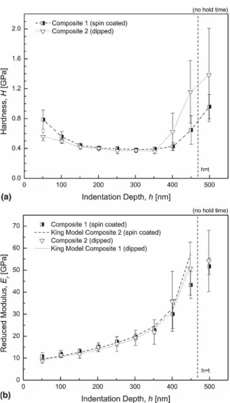
Figure 9 illustrates the results of the hardness meas-urements and the modulus profiles of the spin-coated and the dipped composite films of a similar thickness
FIG. 7. XRD 2D-pole figures of the Laponite (001) basal reflection (Schmidt projection with angles between 0 and 60°) of (a) films prepared by dipping and (b) spin coating using 0.05 wt% PDDA solution and 0.05 wt% Laponite suspension.
FIG. 8. (a) Hardness and (b) reduced modulus profile plots of the spin-coated composite film (0.05 wt% PDDA solution and 0.05 wt% Laponite suspension, 150 bilayers, 460 ± 30 nm film thickness) in comparison to the pure PDDA film (3 wt% PDDA water solution, 300 ± 100 nm film thickness) on silicon substrate as a function of the indentation depth.
(460 ± 30 nm). Note, that due to the significantly lower surface roughness, the spin-coated film of the same thickness contained 150 bilayers, while the dip-coated contained only 135 bilayers. It also has to be noted that
in comparison to Fig. 8 the underlying load functions do not include a hold time. Both films exhibit the above-mentioned U-shaped hardness curve with equal values in the plateau region.
The reduced modulus increases steadily from 11 GPa at 50 nm to 52 GPa at 500 nm indentation depth for the spin-coated film and from 9 GPa to 54 GPa for the dipped film. Furthermore, the results of the King analysis for both films are presented in Fig. 9. The film modulus Efwas calculated to be 8.1 GPa for the spin-coated and 7.7 GPa for the dipped composite film (for standard de-viation see Table III).
H and Erof the various films at an indentation depth of approximately 150 nm are compared in Table III. H of the spin-coated film measured with hold time (Table III, line 1) is about 14% lower than the hardness measured without hold time (Table III, line 2). The behavior of Er is similar: a decrease of about 12% can be observed. Comparing the spin-coated (Table III, line 2) to the dipped composite film (Table III, line 3), the spin-coated film exhibits slightly higher hardness and modulus val-ues. Table III also compares the properties of the PDDA and the composite film, indicating that the nanocompos-ite is 6 times harder and exhibits an up to 17 times higher elastic modulus than the “pure” polymer.
IV. DISCUSSION AND CONCLUSION A. Geometrical characteristics
The average measured thickness of clay/polymer bi-layer formed by spin self-assembly with 0.05 wt% PDDA solution and 0.05 wt% Laponite suspension was 3.18 nm with average thicknesses of 1.06 and 2.12 nm for the polymer and the clay sublayers, respectively. It is interesting to compare these thickness values with litera-ture data for the films prepared by dipping. Fan et al.28 reported slightly higher thickness values for dip-coated films prepared with sodium montmorillonite/PDDA us-ing a concentration range similar to the one used in this paper and also measured using ellipsometry. The average bilayer thickness was 4.07 nm, whereas thicknesses of
TABLE III. Hardness H, reduced modulus Er, and film modulus Efof the one-layer PDDA-film made from 3 wt% solution and the spin-coated PDDA-film with 150 bilayers and dipped PDDA-film with 135 bilayers, both made from 0.05 wt% PDDA solution and 0.05 wt% Laponite suspension.
Film h H (GPa) Er(GPa) Ef(GPa)a
Composite 1 (spin-coated)b 152 0.38 ± 0.02 11.5 ± 1.0 6.7 ± 0.8
Composite 1 (spin-coated)c 151 0.44 ± 0.03 13.1 ± 1.1 8.1 ± 1.1
Composite 2 (dipped)c 151 0.42 ± 0.03 11.9 ± 2.0 7.7 ± 0.6
PDDAa
155 0.060 ± 0.009 0.67 ± 0.14 0.39 ± 0.13 Ratio (Composite 1/PDDA)b ⭈⭈⭈ 6 17 17 aAccording to King’s model,3not depending on the indentation depth h.
bLoad function with hold time. cLoad function without hold time.
FIG. 9. (a) Hardness and (b) reduced modulus of the spin-coated film in comparison with the dipped composite film (0.05 wt% PDDA so-lution and 0.05 wt% Laponite suspension, 150 bilayers for spin-coated and 135 bilayers for dipped) on silicon substrate as a function of the indentation depth.
polymer and clay sublayers were 1.547 and 2.563 nm, respectively. Similar values were reported by Kotov et al.20determined by surface plasmon spectroscopy. The clay/ polymer bilayer thickness was 3.9 ± 0.5 nm and for polymer and clay sublayers 1.6 ± 0.4 nm and 2.46 ± 0.5 nm, respec-tively. Kleinfeld and Ferguson7
prepared films with dripping as an analogous to dipping self-assembly method. They re-ported a bilayer thickness value of 3.8 nm measured by ellipsometry, which is in the same range as that given by Fan et al.28and Kotov et al.,20even while working with a much higher concentration of hectorite (0.2 wt%) and PDDA (5 wt%) solutions. From this sublayer thickness, a volume fraction of the inorganic sublayer in the films between 63 vol%20,28 and 67 vol% (this work) can be calculated. The mass fraction of the inorganic material was determined with 60 wt%, which is lower than that reported by Podsiadlo et al.,29 who calculated, from a TGA curve similar in shape, an inorganic loading of a dip-assembled free-standing film with about 80 wt% (∼42 vol%). The present volume fraction of 67 vol% (as calculated from the sublayer thicknesses) appears to be higher than the one measured with TGA. This discrep-ancy can be explained by intercalation of PDDA in the Laponite interlayer connected with an increase in clay mineral thickness (∼20%, see XRD) and with the wavy layer structure of the films (see Fig. 5).
The similar* value of 9.2° from the XRD measure-ments for films prepared both by dipping and spinning is indicative for high ordering of the crystallites in the z direction and similar to the value obtained for a self-supported clay film of a nontronite prepared by vacuum filtration.30
The increase of the basal distance of the Laponite from 12.3 Å in the original Na-form to 14.3 Å is caused by the intercalation of PDDA in the Laponite interlayer through diffusion during the prepa-ration of the PDDA sublayer.17 The same increase in d-spacing was found by XRD measurements after simple exchange of the Laponite with PDDA solution. Exfoli-ated Laponite forms single smectite layers 0.96 nm thick and 25–35 nm in diameter.31 The average value of the clay sublayer thickness might indicate that each clay sub-layer was built up by 2–3 clay mineral sub-layers. The meas-ured * value means that the Laponite clay particles 25–35 nm in diameter are more tilted as it is possible within a flat sublayer 2.1 nm thick. A simple trigono-metric calculation gives an angle of only 4.7°. The wavy geometry of the sublayers (Fig. 5) explains the measured tilting values.
While the films are assembled LBL, different interfer-ence colors are observed as the film thickness increases, suggesting good optical uniformity and indicating a sur-face roughness, which is small relative to the wave-lengths of visible light; similar observations were done for analogous systems.7
The PDDA solution concentration was found to have a
very strong influence on the film surface roughness. Similar influence of PDDA solution concentration on the film roughness has already been observed for the dipping self-assembly film-formation process.32 The higher roughness was explained using increasing concentrations of PDDA with higher amount of PDDA at the surface inducing aggregation of the clay particles and inhomo-geneous incorporation of polymer.
B. Mechanical characteristics
The functional form of the hardness curves is in good agreement with previously reported work on nanoinden-tation of thin polymer composite films.25,28,33 The in-crease in hardness as the indentation depth approaches the film/substrate interface is attributed to the influence of the hard substrate, while the initial decrease in hard-ness is related to surface effects, e.g., surface roughhard-ness. Saha and Nix24found that soft films on hard substrates accommodate all the plastic deformation, while the sub-strates begin to deform only when the indenter is very close to the film/substrate interface. Hence, it can be assumed that the hardness values in the plateau region are not significantly affected by the silicon substrate and therefore represent the “real” film hardness. Fan et al.28 investigated nanostructured montmorillonite/PDDA multilayer films with thicknesses of 267 and 526 nm produced by stepwise alternating PDDA and clay depo-sition from solution. They determined hardness values of 0.42 and 0.32 GPa, respectively, at 20% indentation depth. In the present case 20% indentation depth fall into the initial decrease in hardness. Therefore, the above-mentioned values are compared to our data at 150 nm indentation depth (corresponding to approximately 30% of the film thickness): 0.38 GPa for the spin-coated film with hold time, 0.44 GPa for the spin-coated film without hold time, and 0.42 GPa for the dipped film without hold time.
In contrast to Wang et al.,33 Er does not follow the expected U-shaped curve. They investigated Teflon films in the thickness range of 48.1–1141 nm and found among the above-mentioned U-shaped curve type that, when the film thickness is less than 500 nm, the modulus increases sharply as the film thickness decreases. Fan et al.28 re-ported that the expected U-shaped curve style was not easily observable, especially for the 276-nm nanocom-posite film. Similar to our data, the modulus increased steadily with increasing indentation depth. At 20% in-dentation depth, they found for the 526-nm thin film a modulus of 9.5 GPa. For our films, 20% indentation depth corresponds to approximately 100 nm deep in-dents. Considering only the influence of the elastic prop-erties of the diamond indenter tip [see Eq. (2)], a film modulus of 11.4 GPa for the spin-coated composite (without hold time) can be calculated. This value is
slightly higher than the film modulus reported by Fan et al.28The difference may be attributed to variations in the volume fraction of clay or unequal film thick-nesses.
Several models focusing on the extraction of the “true” film modulus were applied to our data.23,34,35
King’s23 analysis was found to be in good agreement with experi-mental data (see Fig. 9, dashed and dotted lines, respec-tively). In Table III, the results of King’s analysis are presented: the film moduli Ef of 6.7 and 8.1 GPa were calculated for the spin-coated composite measured with hold time and the spin-coated composite film without hold time, respectively. Comparing Ef of the “pure” PDDA sample to the spin-coated composite, an improve-ment of factor 22 could be achieved. As observed for the hardness, there is only a slight difference in modulus between the spin-coated (8.1 GPa) and the dipped (7.7 GPa) nanocomposite film. For both films, Ef is slightly lower than the value reported by Fan et al.28 (9.5 GPa). However, it has to be noted that they did not account for substrate influences.
V. CONCLUSIONS
Different LBL assembly techniques, based on sequen-tial adsorption of oppositely charged compounds, have been established for preparation of multilayered thin films. Currently, the most commonly used method is based on a dip self-assembly process. The disadvantage of this method is that it is extremely time consuming. In contrast, the spin self-assembly method, which is about 10 times faster, allows the rapid production of films. The production of a 100 bilayer film needs less than 2 h compared to about 17 h by dipping. The films show a lamellar but wavy internal layer structure for both meth-ods with the similar quality of textural arrangement of the clay platelets. However, the surface of the spinned film shows extremely low roughness and is much smoother and more homogeneous than the dipped film. The hard-ness and modulus values for spin-coated films are slightly higher than those of the dip-coated films and significantly higher than those of the “pure” PDDA film: the nanocomposite films are 6 times harder (0.4 GPa versus 0.06 GPa) and have 17 times higher elastic modu-lus (6.7 GPa versus 0.39 GPa).
The PDDA solution concentration was found to have a very strong influence on the film surface roughness. To prepare good quality film by the spin self-assembly method, one needs to use diluted solutions of clay and PDDA (0.05 wt%). The average thickness of a clay/ polymer bilayer formed by spin self-assembly from such solutions was measured as 3.18 nm with average thick-nesses of 1.06 nm and 2.12 nm for the polymer and the clay sublayer, respectively, which is comparable to val-ues reached in the dipping procedure.
ACKNOWLEDGMENTS
The authors thank F. Mornaghini and T. Wermelinger (LNM ETH Zurich) for assistance during the microscopi-cal studies and S. Olliges [Laboratory for Nanometal-lurgy (LNM) ETH Zurich] for help carrying out the tex-ture measurements. We thank Dr. R.T. Konradi [Labora-tory for Surface Science and Technology (LSST) ETH Zurich] who made the ellipsometer available for analysis of the films.
REFERENCES
1. Zh. Tang, N.A. Kotov, S. Magonov, and B. Ozturk: Nanostruc-tured artificial nacre. Nat. Mater. 6, 413 (2003).
2. N.A. Kotov: Ordered layered assemblies of nanoparticles. MRS Bull. 26, 992 (2001).
3. M. Rubner: Material Science: Synthetic sea shell. Nature 423, 925 (2003).
4. F. Barthelat, C.M. Li, C. Comi, and H.D. Espinosa: Mechanical properties of nacre constituents and their impact on mechanical performance. J. Mater. Res. 21, 1977 (2006).
5. F. Barthelat, H. Tang, P.D. Zavattieri, C-M. Li, and H.D. Espinosa: On the mechanics of mother-of-pearl: A key feature in the mate-rial hierarchical structure. J. Mech. Phys. Solids 55, 306 (2007). 6. G. Decher and J-D. Hong: Buildup of ultrathin multilayer films by
a self-assembly process. 1. Consecutive adsorption of anionic and cationic bipolar amphiphiles on charged surfaces. Makromol. Chem. Macromol. Symp. 46, 321 (1991).
7. E. Kleinfeld and G. Ferguson: Stepwise formation of multilayered nanostructural films from macromolecular precursors. Science 265,370 (1994).
8. K. Ariga, Y. Lvov, I. Ichinose, and T. Kunitake: Ultrathin films of inorganic materials (SiO2 nanoparticle, montmorillonite micro-plate, and molybdenum oxide) prepared by alternate layer-by-layer assembly with organic polyions. Appl. Clay Sci. 15, 137 (1999).
9. S. Deville, E. Saiz, R.K. Nalla, and A.P. Tomsia: Freezing as a path to build complex composites. Science 311, 515 (2006). 10. F. Bennadji-Gridi, A. Smith, and J.P. Bonnet: Montmorillonite
based artificial nacre prepared via a drying process. Mater. Sci. Eng., B 130, 132 (2006).
11. C.J. Brinker, Y.F. Lu, A. Sellinger, and H.Y. Fan: Evaporation-induced self assembly: Nanostructures made easy. Adv. Mater. 11, 579 (1999).
12. R.J. Gibbs: Error due to segregation in quantitative clay mineral x-ray diffraction mounting techniques. Am. Mineral. 50, 741 (1965).
13. L. Zevin and W. Viaene: Impact of clay particle orientation on quantitative clay diffractometry. Clay Miner. 25, 401 (1990). 14. J. Cho, K. Char, H. Kookheon, H. Jong-Dal, and Ki-B. Lee:
Fab-rication of highly ordered multilayer films using a spin self-assembly method. Adv. Mater. 13, 1076 (2001).
15. P.A. Chiarelli, M.S. Johal, J.L. Casson, J.B. Roberts, J.M. Robinson, and H-L. Wang: Controlled fabrication of polyelectrolyte multi-layer thin films using spin-assembly. Adv. Mater. 13, 1167 (2001). 16. P.Y. Vuillaume, K. Glinel, A.M. Jonas, and A. Laschewsky: Or-dered polyelectrolyte “multilayers”. 6. Effect of molecular param-eters on the formation of hybrid multilayers based on poly(dial-lylammonium) salts exfoliated clay. Chem. Mater. 15, 3625 (2003).
17. K. Glinel, A. Laschewsky, and A.M. Jonas: Ordered polyelectro-lyte “multilayers”. 3. Complexing clay platelets with polycations of varying structure. Macromolecules 34, 5267 (2001).
18. K. Glinel, A. Laschewsky, and A.M. Jonas: Ordered polyelectro-lyte “multilayers”. 4. Internal structure of clay-based multilayers. J. Phys. Chem. B 106, 11246 (2002).
19. N.A. Kotov, S. Magonov, and E. Tropsha: Layer-by-layer self-assembly of aluminosilicate-polyelectrolyte composites: Mecha-nism of deposition, crack resistance, and perspectives for novel membrane materials. Chem. Mater. 10, 886 (1998).
20. N.A. Kotov, T. Haraszti, L. Turi, G. Zavala, R.E. Geer, I. Dekany, and J.H. Fendler: Mechanism of and defect formation in the self-assembly of polymeric polycation-montmorillonite ultrathin films. J. Am. Chem. Soc. 119, 6821 (1997).
21. W.C. Oliver and G.M. Pharr: An improved technique for deter-mining hardness and elastic modulus using load and displacement sensing indentation experiments. J. Mater. Res. 7, 1564 (1992). 22. M.F. Doerner and W.D. Nix: A method for interpreting the data
from depth-sensing indentation instruments. J. Mater. Res. 1, 601 (1986).
23. R.B. King: Elastic analysis of some punch problems for a layered medium. Int. J. Solids Struct. 23, 1657 (1987).
24. R. Saha and W.D. Nix: Effects of the substrate on the determina-tion of thin film mechanical properties by nanoindentadetermina-tion. Acta Mater. 50, 23 (2002).
25. P.V. Pavoor, A. Bellare, A. Strom, D.H. Yang, and R.E. Cohen: Mechanical characterization of polyelectrolyte multilayers using quasi-static nanoindentation. Macromolecules 37, 4865 (2004). 26. L. Gan, B. BenNissan, and A. BenDavid: Modelling and finite
element analysis of ultra-microhardness indentation of thin films. Thin Solid Films 291, 362 (1996).
27. T.D. Fornes and D.R. Paul: Modelling properties of nylon 6/clay nanocomposites using composite theories. Polymer 44, 4993 (2003).
28. X.W. Fan, M.K. Park, C.J. Xia, and R. Advincula: Surface struc-tural characterization and mechanical testing by nanoindentation measurements of hybrid polymer/clay nanostructured multilayer films. J. Mater. Res. 17, 1622 (2002).
29. P. Podsiadlo, Z. Tang, B.S. Shim, and N.A. Kotov: Counterintui-tive effect of molecular strength and role of molecular rigidity on mechanical properties of layer-by-layer assembled nanocompos-ites. Nano Lett. 7, 1224 (2007).
30. A. Manceau, D. Chateigner, and W.P. Gates: Polarized EXAFS, distance-valence least-squares modelling (DVLS), and quantita-tive texture analysis approaches to the structural refinement of Garfield nontronite. Phys. Chem. Miner. 25, 347 (1998). 31. R.G. Avery and J.D.F. Ramsay: Colloidal properties of synthetic
hectorite clay dispersions. II. Light and small angle neutron scat-tering. J. Colloid Interface Sci. 109, 448 (1986).
32. B. Van Duffel, R.A. Schoonheydt, C.P.M. Grim, and F.C. De Schryver: Multilayered clay films: Atomic force micros-copy study and modeling. Langmuir 15, 7520 (1999).
33. J. Wang, F.G. Shi, T.G. Nieh, B. Zhao, M.R. Brongo, S. Qu, and T. Rosenmayer: Thickness dependence of elastic modulus and hardness of on-wafer low-k ultrathin polytetrafluoroethylene films. Scripta Mater. 42, 687 (2000).
34. X.Z. Hu and B.R. Lawn: A simple indentation stress-strain rela-tion for contacts with spheres on bilayer structures. Thin Solid Films 322, 225 (1998).
35. I.L. Jäger: Comment on: “Effects of the substrate on the determi-nation of thin films mechanical properties by nanoindentation” by Saha and Nix [Acta Mater. 50, 23 (2002)]. Scripta Mater. 47, 429 (2002).