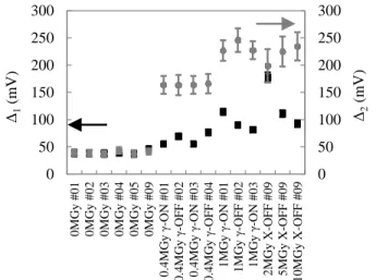
Multi-MGy total ionizing dose induced MOSFET variability effects on radiation hardened CMOS image sensor performances
Texte intégral
Figure

Documents relatifs
The first version of the WEEE Directive had as objectives: to (I) prevent the generation of e-waste; (II) reduce the amount of e-waste by means of reuse, recycling, and other forms
Elles constituent notamment une cause majeure de complication des soins de santé avec, en conséquence, une augmentation de la mortalité et de la morbidité, une
Les mesures de vitesse perpendiculaire effectuées lors du choc 43413 (paragraphe précé- dent) sont ici comparées à celles d’un choc effectué dans des conditions plasma
2- Sélectionner les grandeurs en abscisse et en ordonnée A l’aide de la souris (clic gauche), déplacer l’icône (sonomètre/micro ou temps) sur
Restoration of Generalized Poisson-Gaussian data: The convexity re- sult presented here allows us to address the problem of denoising data corrupted by Generalized
Artistes variés, Dans la rue vol.l, [Disque compact audio], Indépendant, 2003... Artistes variés, Dl'Osti de bon stock, [Disque compact audio],
Numerous small scale applications have been developed for vibration and noise control. These typically precede the full scale development and serve as proof-of-concept for new
13 shows this single point energy profile for the Hemicarboxonium interacting with a SWNT as a function both of the SWNT – Hemicarboxonium distance and the torsion angle the rings
