HAL Id: hal-01787067
https://hal.archives-ouvertes.fr/hal-01787067
Submitted on 7 May 2018HAL is a multi-disciplinary open access archive for the deposit and dissemination of sci-entific research documents, whether they are pub-lished or not. The documents may come from teaching and research institutions in France or abroad, or from public or private research centers.
L’archive ouverte pluridisciplinaire HAL, est destinée au dépôt et à la diffusion de documents scientifiques de niveau recherche, publiés ou non, émanant des établissements d’enseignement et de recherche français ou étrangers, des laboratoires publics ou privés.
Preparing the future post-mortem analysis of
beryllium-based JET and ITER samples by
multi-wavelengths Raman spectroscopy on implanted
Be, and co-deposited Be
M. Rusu, C. Pardanaud, Y. Ferro, G. Giacometti, C. Martin, Y. Addab, P.
Roubin, M. Minissale, L. Ferri, F. Virot, et al.
To cite this version:
M. Rusu, C. Pardanaud, Y. Ferro, G. Giacometti, C. Martin, et al.. Preparing the future post-mortem analysis of beryllium-based JET and ITER samples by multi-wavelengths Raman spectroscopy on im-planted Be, and co-deposited Be. Nuclear Fusion, IOP Publishing, 2017, 57, pp.076035. �10.1088/1741-4326/aa70bb�. �hal-01787067�
Preparing the future post-mortem analysis of beryllium-based JET and
ITER samples by multi-wavelengths Raman spectroscopy on implanted Be,
and co-deposited Be
M. I. Rusua,b, C. Pardanaudb*, Y. Ferrob, G. Giacomettib, C. Martinb, Y. Addabb, P. Roubinb, M. Minissaleb,f, L. Ferryb,c, F. Virotc, M. Barrachin c, C P Lungud, C Porosnicud, P Dincad, M Lungud,
M. Köppene, P. Hansene, Ch. Linsmeiere
a
National Institute of R&D for Optoelectronics INOE 2000, Ilfov, Romania
bAix-Marseille Université, CNRS, PIIM UMR 7345, 13397, Marseille, France
c Institut de Radioprotection et Sûreté Nucléaire, B.P. 3, 13115 Saint Paul-lez-Durance Cedex, France dNational Institute for Laser, Plasma and Radiation Physics, 077125, Magurele-Bucharest, Romania e Forschungszentrum Jülich GmbH, Institut für Energie- und Klimaforschung - Plasmaphysik, 52425 Jülich,
Germany
fAix-Marseille Université, CNRS, Centrale Marseille, Institut Fresnel UMR 7249, 13013 Marseille, France
*
Corresponding author: cedric.pardanaud@univ-amu.fr
Abstract
This study demonstrates that Raman microscopy is a suitable technique for future post mortem analyses of JET and ITER plasma facing components. We focus here on laboratory deposited and bombarded samples of beryllium and beryllium carbides and start to build a reference spectral
databases for fusion relevant beryllium-based materials. We identified the beryllium phonon density
of states, its second harmonic and E2G and B2G second harmonic and combination modes for defective
beryllium in the spectral range 300-700 and 700-1300 cm-1, lying close to Be-D modes of beryllium hydrides. We also identified beryllium carbide signature, Be2C, combining Raman microscopy and
DFT calculation. We have shown that, depending on the optical constants of the material probed, in
depth sensitivity at the nanometer scale can be performed using different wavelengths. This way, we
demonstrate that multi-wavelength Raman microscopy is sensitive to in-depth stress caused by ion implantation (down to ≈30 nm under the surface for Be) and Be/C concentration (down to 400 nm or more under the surface for Be+C), which is a main contribution of this work. The depth resolution reached can then be adapted for studying the supersaturated surface layer found on tokamak deposits.
I. Introduction
The aim of this work is to demonstrate that Raman microscopy is a well-suited technique for future post-mortem analysis of the future ITER and JET walls. Using different laboratory samples, we herein set-up the basis of an experimental methodology in order for Raman microscopy to be used as a characterization technique.
Plasma facing components (PFCs) as first wall are subject to high heat loads and ion irradiation. Therefore it is crucial for a future fusion power plant to understand and predict the evolution of the first wall [1]. The PFC of the future international reactor ITER that will receive most of the particle flux and/or heat loads is the tungsten divertor, while the other PFCs will be composed of beryllium [2]. Some tokamaks are already working nowadays in an ITER-Like-Wall (ILW) configuration in order to prepare the ITER project, such as the Joint European Torus/JET tokamak in which some PFCs are composed of tungsten coated carbon tiles [3-5]. Carbon tiles were used in the carbon era of tokamaks and are still used in stellerators like Wendelstein 7-X. Nowadays carbon becomes more and more unpopular to limit tritium retention [6, 7]; they nevertheless remain a source of carbon contamination for beryllium and tungsten materials in nowadays tokamaks. This will not be true for the ITER tokamak where O and N impurities will be the main problems. In that framework, the surface composition and morphology modifications under operation will lead to changes in the material properties, some of them related to safety issues; these changes will have to be measured and understood. The lifetime of these PFCs and their fuel retention properties will be influenced by the migration [8] and/or melting of elements in the machine [9, 10], the production of dust, the hydrogen isotope retention [11, 12], the complex surface erosion mechanisms, and the impurity contamination (traces of carbon and/or oxygen, nitrogen seeding [13],...) leading to formation of new mixed materials/phases. Surface characterisation techniques are then necessary to measure the elemental changes in JET and in ITER.
Due to their isotope selectivity, Ion Beam Analyses (IBA) play a prominent role in this characterization, as discussed in [14, 15]. Thermal Desorption Spectroscopy (TDS) also plays a role as it gives an indirect access to the characterization of D or T trapping energies in metals such as Be [16-18] or W [19]. These trapping energies are usually calculated by DFT, associated to a rate-equation modeling and thus can be compared with experimental thermal desorption spectra [20-22]. However, even if TDS and IBA techniques give quantitative information about hydrogen isotope concentration, they give only indirect information about chemical bonding. A direct way to probe the chemical environment is to probe it spectroscopically by means of its vibrational spectrum using Raman microscopy. The vibrational frequencies can also be computed by DFT, which complements the Raman analysis. Raman microscopy is a nondestructive, non-contact, and local (≈1m2 lateral resolution [23]) technique that has been proved to be sensitive to Be stretching modes [24], beryllium
oxide modes [25], bending and stretching tungsten oxide modes [26], BexWy mixed samples density of
states [27], Be-C-W irradiated samples [28], and give information when a pristine material is implanted by hydrogen ions [27, 29, 30]. First Raman analyses in ILW-tokamaks were performed on several molybdenum JET mirrors [27], showing that the technique is sensitive to thin (≈10 nm) deposited layer composed of ≈33% Be, ≈33% C and ≈33% O and to the underlying molybdenum oxidized mirror, the atomic percent being obtained by X-ray Photon spectroscopy (XPS). C-O and C=O modes have been detected in that layer, and defective or beryllium mixed with O and/or C have been found without possibility to identify the phases rigorously up to now, because of a poor benchmarking of the technique for these materials. Raman microscopy can also be able to give information about the hydrogen isotope behavior, by combining IBA, Raman microscopy, Atomic Force Microscopy (AFM) and with the help of DFT modeling. Coupling part of these techniques with Raman microscopy has been done in the past with the carbon made Tore Supra tokamak [31-37]. For Be, an illustration of this complementarity, in [38], is that we have identified with laboratory experiments the growth of BeD2 with dendritic forms appearing subsequently to 2 keV ion
implantation when the Be layer is saturated by implanted D ions. The width of the bands recorded by Raman microscopy suggested that this hydride has grown in a crystalline form which seems to be close to a body centered orthorombic structure with Ibam symmetry as the spectra look like to those
reported in [39], who determined recently the structure by using additionally synchrotron X-ray diffraction. In [38], we have showed that these dendrites appear when the amount of deuterium in the material is higher than ≈ 2 1017 D.cm-2, when the ≈ 40 nm under surface layer is saturated by D.
The paper is organized as follow. In part 2, we present the experimental and theoretical methods. In part 3 we present the results that are divided in four subparts: part II.1 and II.2 are devoted to the analysis of defective beryllium samples, either deposits or implanted deuterium with two implantation geometries, and part II.3 is devoted to the analysis of beryllium carbides. Part II.4 put all the results together to better highlight the spectroscopic parameters that matter. In part 4, we discuss the results and give a conclusion in part 5.
2. Methods
2. 1 Sample preparation
As the aim of this work is to demonstrate that Raman microscopy is a well-suited technique for the post-mortem analysis of the future ITER and JET walls, using various Laboratory samples, we produced tokamak-like samples which are deposits or implanted samples. In deposits, we varied the amount of defects to study the corresponding Raman signature. Depending on the Raman cross sections and the amount of chemical bonds formed by beryllium with impurities, answering the question: "could we detect chemical bonds or crystallographic defects ? " the answer is not necessarily
"yes". For example in [27] we were not able to detect Be-N nor Be-D bonds whereas we were able to do so in [38] by identifying BeD2 hydrides. Then, here by "defects", we mean every kind of defects
that can modify the long range crystallographic order of a pristine crystal, the holy grail to reach with this technique being to be defect-sensitive for every material studied.
Depositions of 400 nm thick Be and co deposited Be+C layers were performed on silicon substrates using the thermionic vacuum arc (TVA) method for which the emission of an electron beam produced by a heated filament is focused using a special Wehnelt device toward an anode connected to a high voltage regulated power supply. More details can be found in [40] and references therein. The TVA plasma spatial localization allows gas injection close to the substrate to be performed during the deposition. Three Be samples were synthesized with different amount of defects (referred to S1, S2 and S3). We used partial pressure of N2 and D2 (in the range 10
-2
to 10-3 Pa) to introduce disorder, the amount of N and D being respectively 3-8 atomic % for sample 1, <0.4 atomic % for sample 2 and no additional gas injection for sample 3 [27]. Then sample 1 contains more defects than sample 2, which itself contains more defects than sample 3. For beryllium carbide samples, partial pressure of the Be/C in the substrate vicinity was also in the same range. We used two ratios: Be/C=0.3 and 1.
We used also a commercial reference sample, from MaTecK, to obtain a Raman spectrum with a low amount of defect tracer (referred as RS, reference sample). The 2keV D-implanted Be samples were prepared in a multi-chamber XPS system by PREVAC under UHV conditions with a base pressure in the low 10-10 hPa range. The system was equipped with a M650 monochromatic X-ray source and a R4000 hemispherical energy analyser, both from VG Scienta. In addition, a UV source type PREVAC UVS 40A2 was attached. Sputter cleaning and implantations were performed by a PREVAC 40E1 ion source. All sample preparations steps were performed in-situ without breaking the vacuum. The Be-samples, from MaTecK, had a size of 10 x 10 mm² and an average surface roughness of Ra<1 µm. The samples, were cyclically cleaned by Ar
+
ion sputtering with 35 keV for 30 min and annealing at 600 °C for 45 minutes, until no surface contaminations were visible in the XP-spectra. Both samples have an implantation area of 3 x 3 mm². With a 1.3 A, we evaluate erosion is 20 nm. The beryllium samples was implanted with a fluency of 3.8 x 10¹⁷ D cm-2. For the fluency calculation a beam composition of 2 % D+ and 98 % D2
+
is assumed [1]. The only detectable surface contamination (by XPS) was a small amount of oxygen, which is estimated to be a few %.
2. 2 Sample characterization
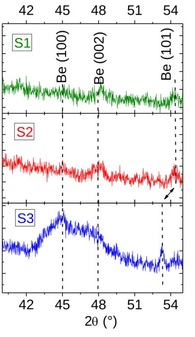
X-ray diffraction was recorded for Be samples (S1, S2 and S3) using a diffractometer provided with a CuKα X-ray radiation source at a wavelength of 1.54 Å. All measurements were performed in the Bragg-Bretano configuration in a long scan from 40o-60o 2θ range with a step size of 0.01o (and 4 s integration time). This interval was chosen to identify the most intense Be peaks, also long integration time was used due to the transparency of Be to X-rays and relatively low thickness of the deposited
layer (36 hours). XR diffractograms of S1, S2 and S3 samples are displayed in appendix A. Grain size dimension was evaluated from the obtained diffraction patterns by recording the ratio between peak area and its corresponding intensity. The peaks related to metallic Be polycrystalline phase were identified and are consistent with crystalline structure of TVA deposited Be with crystalline grains embedded in an amorphous Be matrix, hence the low intensity XRD peaks. Of the three XRD spectra only Sample 3 present all the orientations specific to Be in the analyzed range and additionally the amorphous component of the spectra can be observed due to line broadening of the peaks. Compared to reference XRD data of pure beryllium polycrystalline powder (Be 100 (45.8o), Be 002 (48.44 o) and Be 101 (53.14 o), Samples 1 and 2 exhibit large shifts of Be (101) peak most probably caused by lattice strain induced by D and N atoms. The Be (100) and Be (002) components of sample 1 respectively 2 could not be accurately identified due to low signal per noise ratio. Due to the peaks shape and intensity the grain size dimension could not be accurately estimated from diffractograms but is in the nanosize region. Since the reference material grain size was 10 µm we consider it as infinite compared to sample 1,2 and 3.
RBS measurements on S2 and S3 samples were performed using a broad beam (0.5 mm2) of monoenergetic 2.6 MeV He++ ions focused on the samples at normal incidence. The energy of the backscattered particles was analyzed with a solid state silicon detector (18 keV energy resolution for He particles) positioned at an angle of 165o in respect to the ion beam. In order to extract information regarding the depth profile and elemental distribution, we have simulated the obtained experimental spectra using the SIMRA software [41]. XRD and RBD data are given in appendix A.
Raman spectra were recorded for all the samples using a Horiba-Jobin-Yvon HR LabRAM apparatus in the backscattering geometry (with x100 objective, with a numerical aperture of 0.9 for. L
= 488, 514.5 and 632.8 nm, and x40 for L=325 nm). The Raman mapping mode was also used to get
a signal, and sometimes necessary to increase the signal to noise ratio. The laser power was kept at 1mW m-2. The spectral resolution is typically 1 cm-1. For safety reasons (keeping the surface temperature low to prevent the formation of volatile BeO), we simulated the influence of the power laser on a beryllium sample in air and deposited on a silicon wafer, by taking into account geometric effects, heat diffusion in materials and convection in air, by means of the COMSOL software. The main trend is that working with this power density is safe, but more details of the modeling are given in appendix B.
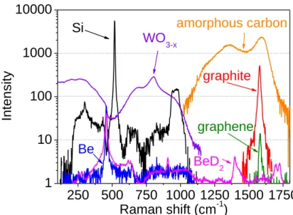
2. 3 Sensitivity/capabilities of Raman microscopy
Briefly, Raman spectroscopy of materials is an inelastic light scattering process that conserves the energy of the incident photon, and the momentum during the scattering process. When the photon produced after scattering has lost energy (Stokes process), the difference in energy is transferred to the vibrational modes of the material. By making the difference between the incident and the diffused photon, one can then obtain the information on the vibrations of the material probed. For crystals, the vibration energy corresponding to phonons (collective modes) is described in a reciprocal space called the Brillouin zone (BZ) where the vibration frequencies depend on the momentum. Because of momentum conservation during the scattering process, and because the momentum of incident light is close to 10-3 Å-1 whereas the one of phonon vary between 0 and 1 Å-1, Raman spectroscopy is only sensitive to the center of the BZ (i.e. phonon momentum close to zero Å-1, called the gamma point). Quantum selection rules governed by crystal symmetry give rise (or not) to some bands related to some vibrational modes. For amorphous materials, long range order no longer exists, and then all the vibrational modes rise. Then the vibrational density of state (called sometimes the PDOS, for Phonon Density of State) is generally observed. As the incident laser beam is focused by a microscope, and as the signal coming from the sample after scattering uses the same microscope, the technique is called Raman microscopy. A deep review of all the capabilities of this technique can be found in [23]. In this part we only give the main ideas in term of sensitivity and spectral windows of relevant materials useful for plasma wall interaction studies in tokamaks and stellerators. Note that we use the following spectroscopic parameters: the band position, labeled , the full width at half maximum, labeled , and some relative intensity ratio between two relevant bands (see below for details). Figure 1 displays Raman spectra of such materials. They have been acquired in the same experimental conditions, using the same experimental set-up, to allow their intensities to be compared and to give a concrete idea which materials can be measured easily or not and under which experimental conditions. One has to note that this plot does not give directly the Raman cross sections, as to determine them it should be necessary to take into account the geometry of the set up used, the optical constants of the materials and to calibrate the detector, which is not under the scope of this work. The wavelength used here is L=514 nm, the objective is a 100x with numerical aperture of 0.9, grating is 600 grooves per mm and
we used backscattering geometry.
The conditions of acquisition known to give very intense Raman spectra were 60 seconds of integration without averaging for bulk silicon, graphite and 200 nm thick hydrogenated amorphous carbon layers [36]. For tungsten oxide layers, graphene (one layer on top of silicon) and bulk beryllium, the acquisition time was also 60 seconds but averaged 150 times in order to increase the signal to noise ratio. For BeD2, an average of ≈ 250 spectra was necessary.
For silicon crystal, the phonon mode at 520 cm-1
is known to give a very intense Raman band that we use here for calibration (it is also used as a wafer for the Be+C codeposits). Features at 300, 640 and 950 cm-1 are roughly one to two orders of magnitudes less intense than the 520 cm-1 band, and are due to combination modes and overtones [42-44].
For 200 nm thick hydrogenated amorphous carbon layers (a-C:H) the well known D and G broad bands are intense. They correspond to aromatic carbons and can give information on defects, nanometric clustering and hydrogen content (see [45] and references there in). For graphite, the stretching mode of C-C bonds is known to give only one Raman band lying
at 1582 cm-1 [46]. This band is less intense than that of the a-C:H, due to differences existing in optical constants (i. e. graphite absorbs more than a-C:H [47]). Note that the full width at half maximum (noted hereafter ) of the bands related to a-C:H are higher by an order of magnitude than that of graphite, then one can estimate the degree of disorder, as it is discussed in [48].
For graphene on top of silicon, the stretching mode of C-C bonds also display a band at 1582 cm-1 which is less intense by more than one order of magnitude, but that can be detected by standard setups.
For 200 nm thick tungsten oxide layer grown under O2 atmosphere at 400°C on top of
tungsten (see [30] for more details), is one order of magnitude lower than silicon. It is roughly composed of two broad bumps, below and above 500 cm-1. The last one is composed of three overlapping bands at approximately 700, 800 and 960 cm-1. The first and second ones are due respectively to transverse and longitudinal optical phonons, and the shoulder at 960 cm-1 is attributed to W=O terminal bonds (see [49] and references therein for more details).
For beryllium, the stretching mode of Be-Be bonds is known to give only one Raman band at ≈ 450 cm-1
in the 100-1100 cm-1 spectral window. Broad bands lying at 645, 887 and between 1008 and 1113 cm-1 have been attributed to defect induced bands in [27]. We will investigate it deeper when describing figure 3. Note that the band at 450 cm-1 has a E2G symmetry
according to point group theory. Beryllium also display a band that is infrared active and that belongs to the B2G symmetry. To put it in a nutshell, symmetry of a crystal atomic structure
can be described by symmetry operations forming group space. Mode symmetry at the gamma point of the Brillouin zone, deduced from the point group symmetry of the given crystal, allow to determine if a mode will be Raman active or not.
For BeD2, 3 groups of bands were found, as shown in [39]. In a recent study we found the
same groups of bands at 270, 615, 909 cm-1, but we also observed a group of two bands at 1710 cm-1 which could be related to surface modes, as the surface to volume ratio was high in our sample, as measured by atomic force microscopy [38] , The 270, 615 and 909 cm-1 groups may be due to a BeD2 close to a body centered orthorhombic structure with Ibam symmetry.
The intensity of all these bands is roughly a factor of two lower than the intensity corresponding to the 1582 cm-1 band of a graphene layer. By taking into account the volume probed by the laser for BeD2, (100-200 nm depth penetration as evidenced in [38]) and
compared to the monoatomic layer of graphene, then we can conclude that the Raman cross section is ≈300 times smaller in the case of BeD2 than in the case of graphene.
These spectroscopic features will be used in order to assess and determine defects and impurities in beryllium based materials.
250 500 750 1000 1250 1500 1750
1
10
100
1000
10000
Be
BeD
2WO
3-xSi
graphene
graphite
In
te
n
s
ity
Raman shift (cm
-1)
amorphous carbon
Figure 1. Raman spectra of materials relevant for plasma wall interactions . All spectra were
recorded in the same experimental conditions. See the text for details. Silicon is used as a reference.
L=514 nm.
2. 4 Computational details
The calculations in this work are based on DFT as implemented in the Quantum Espresso Package [50] with thePerdew-Burke-Ernzerhof functional (PBE)[51]. The details and results of the electronic structure calculation were presented elsewhere in a previous paper [46].
Herein we calculated the vibrational properties of beryllium carbide in the formalism of the Density Functional Perturbation Theory [52], still as implemented in Quantum Espresso. Calculations were performed at the -point only in order to be comparable with the Raman data. The band intensity and selection rules were not taken into account in the calculation.
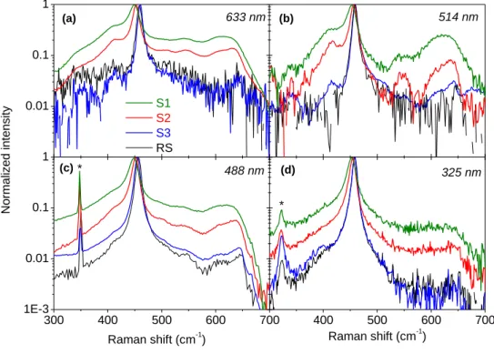
3. Results 3. 1 Nanocrystalline Be deposits 0.01 0.1 1 300 400 500 600 700 1E-3 0.01 0.1 1 400 500 600 700 S1 S2 S3 RS No rm a liz e d i n te n s ity 633 nm (a) (b) 514 nm * (c) Raman shift (cm-1) 488 nm * (d) Raman shift (cm-1) 325 nm
Figure 2. Normalized Raman spectra of deposited samples 1, 2 and 3 (S1, S2 and S3) compared to
commercial Be microcrystal (RS), for four laser excitation wavelengths: (a) 633 nm, (b) 514 nm, (c) 488 nm and (d) 325 nm. The bands marked by stars are due to other electronic transitions from the
laser media.
Figure 2 displays Raman spectra of deposited Be S1, S2 and S3 plus the commercial reference sample RS for 4 laser wavelengths. We focus first on the 633 nm data (Fig. 2-a). The band associated to the E2G Raman active mode is down shifted for S1 and S2 whereas it is lying at 458 cm
-1
for both S3 and RS. Be for S3 and RS are close to 8 cm
-1
, meaning the amount of defects is close for these two samples. For S1 and S2, it is higher (14 cm-1 for S2 and 27 cm-1 for S1). The logarithmic scale used here allows to distinguish several additional broad bands (413, 544 and 616 cm-1) that were first evidenced in [27], and called defect induced bands. As explained in [27], all these bands are similar whatever D or N being included in the material, meaning these bands are not directly related to Be-D or Be-N vibrators, but their inclusion produces defects in the crystal giving rise to these bands, which are interpreted as Phonon Density of States (PDOS).. Selection rules are relaxed by defects as defects break the translational symmetry of the crystal. As a consequence, part of the full PDOS is revealed
thanks to defects, leading to additional bands in the Raman spectra. Their intensity, measured by comparing the height of the 620 cm-1 band to the Raman active E2G band at ≈457 cm
-1
and labeled hereafter HPDOS/HBe, reaches values as high as 23 % of the Raman active E2G mode height's. These
bands are more intense for sample 1 than sample 2, which may be related to high defect contents. Note that these bands are also present in the commercial reference and sample 3, with a height as low as 1%. As crystal sizes for these 2 samples are respectively several microns and 19 nm, then the presence of these bands is not related directly to the crystal size. We then conclude that it is related to the defect content inside crystallites, not related to grain boundaries. Defects can include impurities, vacancies, ...
Several differences exist when changing the wavelength: for example, the PDOS area diminishes monotonically with the decrease of the laser wavelength (as it is easier to manipulate, we uses the height of the band which is the more intense and that diminishes from 23% with 633 nm down to 4% with 325 nm for the S1). Be does not display a monotonic evolution with the laser
wavelength nor for S1 nor for S2. It could be due to the local influence of defects that change the Be-Be frequency by changing the electronic structure and/or the bond length. For RS, which has an amount of defects similar to S3, oppositely, does not disperse in the range 325 - 633 nm. From that we can conclude that the shifts observed for S1, and S2 are due to stress [23] in the deposited layer, the non monotonic behavior being caused by two effects: stress gradients existing in the deposited layers and the penetration depth of the laser that is wavelength dependent. These points will be investigated in more details on the part focused on implanted samples.
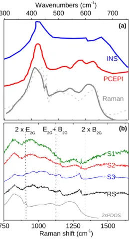
300 400 500 600 700 750 1000 1250 1500 (b) INS PCEPI Raman (a) Wavenumbers (cm-1) RS S3 S2 E 2G+ B2G 2 x B2G Raman shift (cm-1) 2 x E2G S1 2xPDOS
Figure 3. Be phonon density of states (a) and 2nd harmonic PDOS (b) spectral regions. In (a), the
phonon density of states is obtained directly by using INS and PCEPI methods [53]. We derive the PDOS from Raman spectra after removing the E2G Raman active mode to the total spectrum (sample 1
and 2 are used here, with full and dashed grey lines, respectively. The PDOS obtained for sample 3 is not shown because of a low signal to noise ratio).
Figure 3-a (spectral range 300-750 cm-1) displays the PDOS of beryllium crystals as measured in the literature [53] by Neutron Scattering (INS) or Point Contact Electron Phonon Coupling Interaction (PCEPI), and compared to two Raman spectra (S1 and S2, containing defects). To obtain these Raman spectra, a multiple band fit has been done close to 458 cm-1 before the band corresponding to the E2G mode has been subtracted. One can see the good agreement between these
spectra and the PDOS, allowing us to claim that these bands are due to the PDOS. Differences exist between the PDOS of the two samples obtained with Raman spectroscopy, which can be related to different stress existing in the layer, as was also pointed out when describing figure 2. Obtaining quantitative information from that observation is not under the scope of this work but could be the objective of a next work.
Figure 3-b displays the 750-1700 cm-1 spectral range for S1, S2, S3 and RS. This range is of interest for the following reason: frequencies measured by Raman spectroscopy correspond to the
transition of a given oscillator from the vibrational ground state, noted v0, to the first exited state, noted v1. A double excitation from v0 to v2 (called second harmonic for vibrators, and 2PDOS for crystals) might happen, which is characterized by approximately twice the frequency from v0 to v1. Because of selection rules, the intensity of such transition is much lower, because of anharmonicity, the corresponding frequency is lower than twice the single excitation frequency. 750-1700 cm-1 is the range where second harmonics are observed for beryllium, it is also the range where Be-D vibrational modes could fall in deuterium containing beryllium samples. In Figure 3b, the wavenumbers of the expected second harmonic 2E2G, E2G+B2G and 2B2G modes (vertical lines) together with the second
harmonic PDOS have been displayed (merely multiplying by two the wavenumbers of the PDOS displayed in Figure 3-a) and are compared to the Raman spectra of S1, S2, S3 and RS. The broad bands of S1 at 829, 935, 1043 and 1253 cm-1 are very close to the one of the 2PDOS. The relative intensity ratios are slightly different, which can be attributed to anharmonic effects. Phonon calculations based on DFT may be useful for a better understanding, but they are highly time consuming when performed on the full Brillouin Zone on a dense grid of k-points to yield a well-converged PDOS. On both the reference sample and sample 3, which are the ones with less disorder, two other narrower bands can be observed at 1151 and 1296 cm-1. They fall close to the E2G+B2G and
2B2G, at +23 and -40 cm -1
from the harmonic wavenumbers, respectively. Note that these bands are not observed for S1 and S2 which display more defects. To summarize, these narrow bands are due to a more ordered crystal and the shifts are due to anharmonic effects.
3. 2 Be implanted by D: in depth defect sensitivity
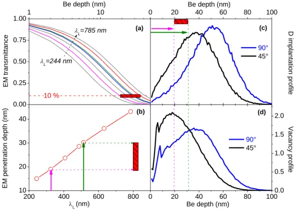
We have also studied the influence on the Raman response of ion implantation in beryllium polycrystals. To tune the amount of defects created under the surface, two impinging ion geometries were used at 2 keV/D: normal incidence (90°) and 45° incidence. Note that the 90° geometry was the one used in our previous study [38], that was focused on the formation of beryllium hydride dendrites at high fluences. D implantation and vacancy creation profiles have been evaluated using the SRIM code. This code is widely used to investigate ion-surface interaction phenomena. It is a free access Monte-Carlo computer program based on the binary collision approximation that do not take into account crystal structure or vacancy diffusion (i.e. each single collision event is treated independently between two steps) [54]. Attenuation of light has been evaluated using the imaginary part of the refractive index, k [55], to deduce the electromagnetic (EM) transmittance T=exp(-4ek/) for a given wavelength at a given depth, e. All the information needed to interpret Figure 5 are displayed in Figure 4, which shows the penetration of light and ions as a function of depth.
Figure 4-a displays the EM transmittance from 244 to 785 nm in beryllium: the higher the wavelength, the deeper the light penetrates. We define a criteria corresponding to a 90% attenuation
intensity (corresponding to a transmittance of 10 %) for a given wavelength. This criterion is purely arbitrary and has been defined to give an idea of the electromagnetic field penetration depth. Figure 4-b displays that values for all the wavelengths. The D implantation and vacancy profiles are displayed in figure 4-c and 4-d, respectively. This allows to estimate that 16 % of the deuterium atoms are implanted in the range 0-19 nm, 31% in the range 0-28 and 37% in the range 0-31 nm. For the same ranges, the amount of vacancies created are respectively 37%, 59% and 65 % of the total amount of vacancies created. The average density of vacancies (calculated by integrating from 0 to a given depth and dividing by the slab thickness used for a given wavelength) is the higher in the range 0-28 nm, being lower by 7.6% in the 0-19 nm range and by 0.4% in the 0-31 nm range. Note that Raman spectroscopy is sensitive to a part of the implantation profile because the implantation depth and the optical properties of the material both fit well. The message here is to say that this technique will be useful for Be mainly to probe the very near surface of deposits (supersaturated layer) or implanted samples in tokamaks, but it will not be sensitive to the bulk (hundreds of nm to microns).
0.00 0.25 0.50 0.75 1.001 10 0 20 40 60 80 100 200 400 600 800 10 20 30 40 0 20 40 60 80 1000.0 0.5 1.0 1.5 2.0 (a) (d) (b) Be depth (nm) L=785 nm L=244 nm EM t ra n s m itt a n c e (c) 10 % Be depth (nm) 90° 45° D i m p la n ta ti o n p ro fi le EM p e n e tra ti o n d e p th (n m ) L (nm) 90° 45° Va c a n c y p ro fi le Be depth (nm)
Figure 4. Comparison of in depth penetration of electromagnetic wave implanted D ions. (a) The
transmittance is plotted for 244, 325, 407, 488, 514, 633 and 785 nm. The red rectangle is for the wavelengths used in this study (325-514 nm). An arbitrary extinction criterion is defined as when the transmittance equals 10%. (b) Using this criterion, the penetration depth is plotted as a function of the
(normal to the surface or at 45° to the surface). Kinetic energy is 2 keV. Calculation was made with SRIM.
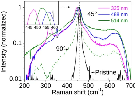
In figure 5 we compare the 514 nm spectra of RS pristine Be, a Be sample containing 2 1017 D cm-2 in the 90° geometry and the 325, 488 and 514 nm spectra of RS pristine Be sample in the 45° geometry. Two main findings can be highlighted here:
We first focus on the comparison between 45° and 90° geometries, recorded using the 514 nm laser. We see that the Be implanted by D in the 90° geometry displays a Raman spectrum with a E2G mode downshifted by 5 3 cm
-1
and with an additional broadening of 6.5 cm-1 compared to the pristine sample. The PDOS feature is present, with a relative height ratio of HPDOS/HBe
=3 6 %. If we compare with the Be implanted by D in the 45° geometry, we see that the band corresponding to the E2G mode is downshifted by 5 cm
-1
, with an additional broadening of 30 cm-1 compared to the pristine sample. The PDOS feature is present, with a relative height ratio HPDOS/HBe of 24%. The band position is the same in the two implantation geometries.
However the band width Be is increased by a factor 2.7 and the PDOS relative height
HPDOS/HBe is increased by a factor 11 from the 90° to the 45° geometry. How these differences
can be interpreted ? According to SRIM calculations in the range 0 down to 31 nm there are more defects (implanted D and vacancy) created in the 45° geometry than in the 90° geometry. Then, it explains why HPDOS/HBe and Be are higher in the first case than in the second, and the
band is more downshifted in the first case than in the second.
We now focus on the depth-dependency characterization of the 45° geometry sample using the 325, 488 and 514 nm lasers: in figure 5,Be=448 cm
-1 for 325 nm,Be=456 cm -1 for 488 nm andBe=453 cm -1
for 514 nm, which is not evolving monotonically with the laser wavelength (see inset of figure5). A downshift can be interpreted as a tensile stress in the material, that can be due to defects or impurities, according to [23]. Then, we can say that the tensile stress is more pronounced in the first 19 nm below the surface as the 325 nm laser gave the lowest value ofBe. This tensile stress is less important in the zone 19-28 nm and increases slightly in
the range 28-31 nm, according to the values ofBe. What can cause this shift and stress ? Two
candidates are the presence of vacancies and implanted deuterium that can create chemical bonds changing the bond lengths [56], [38]. However, we were not sensitive enough to detect the presence of Be-D bonds, directly. We were only able to detect Be-Be bonds modification (band shift), which may be an indirect effect caused by the presence of Be-D bonds close to the Be-Be bonds (the reader can see a discussion on that point in [38], where we were able to couple direct and indirect effects on a sample). A systematic thermal study using Raman spectroscopy plus thermal desorption spectroscopy of implanted samples may help in
detecting the formation or release of D from Be-D bonds, like we did in [36]. However the small change in vacancy concentration can be responsible for the Be variation observed using
the 3 wavelengths. In the past, tensile stress gradients have already been observed using Raman spectroscopy on bombarded diamond, and it has been correlated to both the presence of vacancies and implanted species [57].
200
300
400
500
600
700
0.01
0.1
1
Pristine
90°
*
In
te
n
s
ity (
n
o
rm
a
liz
e
d
)
Raman shift (cm
-1)
*
325 nm 488 nm 514 nm45°
445 450 455 460Figure 5. Normalized Raman spectra of D implanted Be samples. Geometry implantation (90° and
45°) are compared with the 514 nm laser excitation. The 45° implanted sample is also analyzed with 488 nm and 325 nm laser excitations.
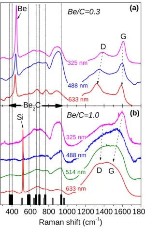
3. 3 Be+C codeposits: Be2C identification 400 600 800 1000 1200 1400 1600 1800 Be/C=1.0 (b) 633 nm 488 nm 325 nm (a) Be/C=0.3 Be Be2C 633 nm 514 nm 488 nm G D Raman shift (cm-1) Si 325 nm G D
Figure 6. Multiwavelength Raman spectra of codeposited Be+C samples. The Be/C flux is 0.3 (a). The
Be/C flux is 1.0 (b). Calculated vibrational modes are also displayed, for comparison. Bars in black correspond to our calculations, bars in grey correspond to calculations from [58].
Figure 6 displays the Raman spectra of Be/C co-deposits. We performed only two different deposition conditions in order to give the reader an idea of what can change from one kind of deposit to another kind of deposit, only changing one parameter, here the Be/C ratio. Note that studying systematically how the Be/C ratio (or other parameters [59, 60]) impact on the materials obtained (structure, texture, gradient concentration, columnar growth [61]...) is not under the scope of this study. Figure 6-a displays the results with a flux ratio of Be/C=0.3 whereas Figure 6-b displays the results with a flux ratio of Be/C=1. In both graphs, two spectral windows can be distinguished: lower than 1100 cm-1 and higher than 1100 cm-1. When the Raman shift is higher than 1100 cm-1, two bands, called the D and G bands, are present. These bands are representative of amorphous or nanocrystalline sp2 carbons. The D and G band have been presented in section 2.3 and are due to aromatic bonds. The D band disperses in both Figure 6-a and-b whereas the G band only disperses in Figure 6-b where the bands are broader and overlapped. The interpretation is that the carbon phase is more disordered in the
case of Figure 6-b than in the case of 6-a, being nanocrystalline in Figure 6-a and amorphous in Figure 6-b. The literature about Raman spectroscopy of carbons is very abundant. Here we decided not giving details but more details on information that help in interpreting the spectra can be found in [48, 62].
Below 1100 cm-1 three groups of broad overlapping bands are observed at ≈ 895, 675 and 350 cm-1 in figure 6-a and b whatever the wavelength used. A narrow band is observed at ≈ 444 cm-1 in figure 6-a and 520 cm-1 in figure 6-b. The first narrow band is the E2G mode of Beryllium, but it is
downshifted compared to the bulk beryllium crystal and the second one correspond to the silicon Raman active mode, as shown in Figure 1. The shift of the E2G mode is stronger using L=633 nm than
the other wavelengths, meaning a higher tensile stress exists deeper in the material. The shape of the broad groups of overlapped bands at 895, 675 and 350 cm-1 in figure 6-a and b vary with the wavelength of the laser used, as it will be discussed below. We calculated by DFT the vibrational spectra at the gamma-point of the Be2C structure determined in [63, 64]. For comparison with
experimental data, the calculated frequencies are displayed in Figure 6 as black histograms, since the respective intensity of each peak has not been determined. One can see that there is a good qualitative agreement between the frequencies obtained by DFT calculations and the measurements that allow us to identify the broad groups of bands at ≈ 895, 675 and 350 cm-1 to the Be2C phase. In more details,
calculations predict the existence of modes with frequencies at 376, 400, 575, 587, 590, 662, 697, 699, 762 and 930 cm-1 (the complete analysis in terms of symmetry and degeneracy is not under the scope of this paper) that can be qualitatively compared to the overlapped bands measured at: 352, 410, 580, 640, 680, 714, 772, 890, 938 cm-1. Some discrepancy remains: for example few cm-1 to ≈20 cm-1 shifts exist. This can be due to the fact that DFT calculations were made taking into account perfect bulk crystal whereas the experimental samples are defective (this is confirmed by the full width at half maximum that are important, which is generally the case for an inhomogeneous material). When comparing experience and theory, such differences are usually expected, too. However one experimental band, lying at 890 cm-1, is not predicted by our DFT calculations (black lines). Previous DFT calculations display modes lying at 511, 639,751, 842 and 966 cm-1 [58]. These calculations were performed for a Be2C monolayer. The corresponding frequencies are displayed in grey in Figure 6. All
the frequencies corresponding to these modes are close to the frequencies of the bands measured experimentally, and cannot be distinguished because of overlapping, except the mode with the frequency being at 842 cm-1. This mode is near the band lying experimentally at 890 cm-1, that we propose to assign to a surface effect, as the calculation in [58] was done for a surface. Then, our interpretation is that our spectra reveal a superposition of bulk and surface Be2C. Not all the
calculation and experimental Be2C modes frequencies fit well. This could be due to some coupling
between phases which is not taken into account in the calculation. However, the spectral domain is the same for calculation and experimental data. One extra point is that the band at 895 cm-1 is more intense than the other bands using 325 nm, and its relative intensity diminished when increasing the
laser wavelength. Postulating that this band is due to a surface contribution (because calculations give the information that the highest wavenumber comes from the monolayer Be2C which can be
considered as a surface), one can conclude that the ratio bulk/surface vary within the depth probed. From that, we found that the crystallite size of Be2C diminishes with depth in the deposit. Obtaining
the precise size of the crystallites is beyond the scope of the study. Also note that the D and G bands are more intense than the Be2C bands using L=633 nm (compared to the other wavelengths), whereas
it is the contrary for the E2G mode of beryllium. It means that there are more carbons deeper in the
material and more Be closer to the surface. For the experimental conditions of figure 6-b the E2G mode
is not observed as a band but the underlying silicon wafer is visible. The carbon phase is observed but on an amorphous form, and the Be2C is also observed. Slight differences are observed by changing the
wavelength and gives a qualitative information about the relative abundances of the different phases as a function of depth. This can be due to slight modification of plasma parameters during the deposit, as said in [65] In figure 6-b the underlying silicon wafer gives a lower signature with lower wavelength meaning its signature is extinguished because of attenuation of light, as shown in [66] on another material. As we see the 520 cm-1 band, one can conclude that all the layer is probed by all the lasers used. As we do not see the 520 cm-1 silicon band for the sample with Be/C=0.3 (Figure 6-a), the layer absorbs more than for the sample with Be/C=1. This is mainly due to a higher organization in the carbon phase, according to [66] and references therein, and also to the presence in one case of Be crystallites. Then, we probably do not probe all the layer in that case. Note that the selection rules were not taken into account in the DFT calculations because the samples are not perfect crystals, and then Raman selection rules may be partially relaxed.
3.4 Relevant spectroscopic parameters 0.05 0.10 0.15 0.20 0.25 10 15 20 25 30 35 40 435 440 445 450 455 460 2 (b) H P D O S / H Be (a) 1 Defects Be ( c m -1 ) Be (cm -1 ) RS S1 S2 S3 90° Impl. 45° Impl. Be+C Tensile stress
Figure 7. Raman parameter plots. (a) HPDOS/HBe as a function of Be. (b) Be in function of Be. The
data were gathered from figure 2, 4, and 6. Lines are guides for the eyes. In the legend, "90° Impl." and "45° Impl." stand for pristine Be implanted by D, "Be+C" stand for Be + C codeposit with Be/C=1 because there is no beryllium band for the Be/C=0.3 sample.
In material science, the full width at half maximum is generally used to deduce how disordered a material is. Figure 7 displays in function of Be relevant spectroscopic parameters for all
the samples and for all the laser excitation wavelengths used in order to give general trends that could be used in the future for JET or ITER post mortem analysis. We have used the full width at half maximum of the E2G mode and its intensity comparison with the intensity of the PDOS signatures as
a probe for determining the relative amount of defects. The frequency of the E2G mode is used for
probing the stress in the material.
Comparing HPDOS/HBe (the height of the PDOS as measured at 620 cm -1
compared to the band related to the E2G mode) and Be in figure 7-a shows that both parameters evolve linearly (when
samples the offset is zero. It can reach up to 2=16 cm -1
for the 45° implanted samples. Then, these two spectroscopic parameters do not probe the same kind of defects as the horizontal shifts depend from one sample to the other. The origin of this difference should be studied by complementary disorder-sensitive techniques in the future, such as positron annihilation spectroscopy [67] or transmission electron microscopy. Figure 7-b display Be in function of Be. The natural width, for a
defect free crystallite is Be =8cm -1
. All the data, whatever the sample, are grouped around two lines: one starting at Be =8cm
-1
with a negative slope, and one with a positive slope. The one with the negative slope shows that when the amount of defect increases then the tensile stress, which is proportional to the band frequency [23], also increases. For Be >30 cm
-1
the slope changes and Be
increases with Be, leading to a compressive stress. There is an exception which is for beryllium
crystallite coexisting with Be2C and C phases: a downshift of the E2G band can coexist with a low
value of Be. Such a high downshift has been previously observed for photon irradiated Be-C-W
samples in [28]. Understanding this point is not under the scope of this paper but could be understood in the framework of dedicated study on coupling between Be, Be2C and C clusters.
4. Summary/Discussion:
This work follows two precedent works [27, 38] where we were able to detect the growth of BeD2 crystals under D implantation conditions. Here we focus on the finger print of defects in the
Raman spectra of Be due to deposition process with some impurities (D2, or N2 atmospheres)
co-deposits (with C) or D implanted samples that generate defects, whatever they are (single interstitial atom, vacancy, di-vacancy, chemical bond creation,...).
To resume the main findings of this study: for defective beryllium (N and D deposits or D implanted samples), the electric field of the laser used to probe the material by means of Raman inelastic scattering penetrates down to ≈ 20 nm using 325 nm and down to ≈ 30 nm using 514 nm laser, allowing to probe macroscopic gradients (such as tensile stress defect concentration,...). This thickness is typically in the same order of magnitude as that of the supersaturated layer found in tokamak deposits [12]. In our spectra, we have identified defect induced bands that are due to the selection rule relaxation caused by these defects, leading to the observation of the PDOS and 2PDOS features in the range 300-1300 cm-1. These bands lye close to Be-D modes of beryllium hydrides or to Be-O modes of beryllium oxide, which can hinder Be-D and Be-O identification/quantification for small amounts of D and O. By comparing D-implantation profile obtained by SRIM calculations, the full width at half maximum of the E2G mode has also been shown to be related to the amount of
defects, being larger when more defects are created. Horizontal shifts in the plot HPDOS/HBe = f(Be)
may be the finger print of some specific defects affecting the full width at half maximum of the E2G mode of Be. Then, to harness this observation, future efforts should be made varying and controlling systematically the kind and amount of such defects.
Then, the main findings for the Be+C codeposit part:
- Three phases can coexist: Be crystallites, carbon phase (amorphous or nanocrystallite) and Be2C phase.
- Their relative concentration vary with the depth of the deposit layer
- Be2C surface and bulk signatures have been identified. We have concluded that crystal size
changes with the depth of the deposit layer
- The organization of the carbon phase (amorphous/nanocrystalline) together with the presence of Be crystallites influence the in-depth information retrieved. It leads to a difficulty for estimating the depth probed because of light absorption.
The term "defects" used in this paper is used as wide as possible, whatever they are (single interstitial atom, vacancy, di-vacancy, chemical bond creation,...). The "holy grail" of this technique would be to identify on spectra the selective fingerprints of each kind of defects, but this is not under the scope of this work, yet. However we give first experimental trends that will help to reach this goal in the future. Then, this work has to be read as a first step, useful to identify the capabilities of Raman microscopy for studying beryllium based materials. As it concerns the propagation of an electromagnetic field in a medium, many phenomena that can modify propagation are involved. It is then difficult to use this technique alone. The interpretation of the multiwavelength Raman microscopy results can be improved in the future by developing multiscale calculations (molecular dynamics) to help interpreting quantitatively band shifts in order to determine precisely the amount of local stress (itself induced by the type defects in the material), as it was done in silicon and germanene [68, 69]. Using other techniques to measure the amount of pollution will also help the understanding of the underlying mechanisms at play. Then, used alone Raman microscopy can give rapidly a huge amount of data at the scale of a tokamak but other techniques are necessary to understand what is really measured in order to interpret correctly the Raman spectra. Biases in the technique can exist depending on the optical constants of the materials probed: if metallic only the first nanometers will be probed (very useful to better characterize the supersaturated layers found in deposits) whereas few microns can be probed for insulators. If the aim is just to give trends and characterize the quantity of defects on some localized surfaces, Raman spectroscopy alone is enough. If a more refined analysis is required, then this technique has to be coupled with other techniques. Some of them are used routinely in the community: ion-beam analysis (IBA) and thermal desorption spectroscopy (TDS) are some of them. IBA is a family of techniques based on high energetic ions (in the MeV range) interacting with
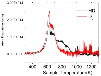
the material probed. Rutherford backscattering (RBS) is one of them and can allow to determine chemical composition. This technique is quantitative and give in-depth information in the range of few microns/tens of microns. However, the in depth resolution is in general not in the range of tens of nanometers, then Raman spectroscopy applied on absorbing materials is a well suited complementary technique, and an example of coupling between IBA and Raman spectroscopy can be found in [31]. In appendix A, we give RBS data on Be samples S2 and S3, which confirms the presence of nitrogen and its uniform distribution in depth for S2. Also, the depth profile of oxygen impurities is observed. The O distribution varies in film depth for both samples, with higher values near the surface and film-substrate interface. Due to poor resolution for low Z elements and information regarding D cannot be obtained by this technique. The D issue has been resolved using TDS performed in a high vacuum chamber (10-9 mbar) with a 10 K stable heating. The desorption chart highlights the HD and D2 signals
measured by the quadrupole mass spectrometer as a function of temperature. D released through BeD2 molecule dissociation has a characteristic peak at 600K, followed by a desorption shoulder in
the 650-720 K resulted most likely by D release from BeO associated trapping-states that were not seen by Raman spectroscopy, may be due to low cross section. HD release at temperatures higher than 800 K confirms the retention of D in high energy traps caused by film defects.
Raman spectroscopy can give information on the chemistry of the sample. Our aim here was not to study from a chemical point of view the thermal stability of the S1 sample, but coupling TDS and Raman on heated samples can give complementary information such as the kind of bonds present in the material at a given temperature, in order to interpret the different TDS peaks. This work can be done in a future work. Other techniques, such as XPS, AFM or electron microscopies, have been also used in the community and examples can be found in the introduction.
5. Conclusion:
Results from the literature in the framework of the ILW JET campaigns, hydrogen isotope content was found higher on the first surface layer, estimated to be a few tens of nm only, and called recently the supersaturated layer. It has been suggested that this layer could be composed of beryllium hydrides, without demonstrating it. Unfortunately the actual ion beam techniques are unable to have access to this in depth resolution. In that work, we benchmarked multiwavelength Raman microscopy on laboratory deposited and implanted samples in order to control the capabilities of this technique. We have shown that on defective beryllium (D-implanted and deposited) we are able to probe ≈ 30
nm. As we are able to detect Be-D bonds, in the case where the optical constants of the probed material allow it (beryllium is metallic) this technique is suitable to be used for the analysis of the
supersaturated layer. In other cases (beryllium mixed with carbon can be an insulator), this technique
can be sensitive to a deeper zone (up to 400 nm). We have also shown that we are able to quantify detect a variation of defects from one sample to another and to retrieve qualitative information about local stress. By comparing DFT modeling with our results, we were also able to identify Be2C Raman
signatures in Be+C codeposits.
Acknowledgements
This work has been carried out within the framework of the EUROfusion Consortium and has received funding from the Euratom research and training programme 2014-2018 under grant agreement No 633053. The views and opinions expressed herein do not necessarily reflect those of the European Commission. This work has also been carried out thanks to the support of the A*MIDEX project (no ANR-11-IDEX-0001-02) funded by the ‘Investissements d’Avenir’ French Government program, managed by the French National Research Agency (ANR). C Pardanaud and MI Rusu acknowledge the Fondation Aix-Marseille Université for funding the postdoctoral postion.C.P.Lungu, C Porosnicu, P. Dinca, M.Lungu acknowledge the funding by the Romanian National Authority for Scientific Research, UEFISCDI, through project number PN-II-ID-PCE-2011-3-0522.
Bibliography
[1] R. Neu, A.U. Team, E.P. Taskforce, J.E. Contributors, Preparing the scientific basis for an all metal ITER, Plasma Physics and Controlled Fusion, 53 (2011).
[2] V. Philipps, Tungsten as material for plasma-facing components in fusion devices, Journal of Nuclear Materials, 415 (2011) S2-S9.
[3] F. Romanelli,et al, Overview of the JET results with the ITER-like wall, Nuclear Fusion, 53 (2013). [4] S. Brezinsek, J.-E. Contributors, Plasma-surface interaction in the Be/W environment: Conclusions drawn from the JET-ILW for ITER, Journal of Nuclear Materials, 463 (2015) 11-21.
[5] S. Brezinsek, A. Widdowson, M. Mayer, V. Philipps, P. Baron-Wiechec, J.W. Coenen, K. Heinola, A. Huber, J. Likonen, P. Petersson, M. Rubel, M.F. Stamp, D. Borodin, J.P. Coad, A.G. Carrasco, A.
Kirschner, S. Krat, K. Krieger, B. Lipschultz, C. Linsmeier, G.F. Matthews, K. Schmid, J.E.T. Contributors, Beryllium migration in JET ITER-like wall plasmas, Nuclear Fusion, 55 (2015).
[6] J. Roth, E. Tsitrone, A. Loarte, T. Loarer, G. Counsell, R. Neu, V. Philipps, S. Brezinsek, M. Lehnen, P. Coad, C. Grisolia, K. Schmid, K. Krieger, A. Kallenbach, B. Lipschultz, R. Doerner, R. Causey, V. Alimov, W. Shu, O. Ogorodnikova, A. Kirschner, G. Federici, A. Kukushkin, E.P.T. Force, I.P. Team, E. Fusion, D.I.V. Itpa Sol, Recent analysis of key plasma wall interactions issues for ITER, Journal of Nuclear Materials, 390-91 (2009) 1-9.
[7] G.F. Matthews, J.E. Contributors, A.S.-U. Team, Plasma operation with an all metal first-wall: Comparison of an ITER-like wall with a carbon wall in JET, Journal of Nuclear Materials, 438 (2013) S2-S10.
[8] I. Bykov, H. Bergsaker, G. Possnert, Y. Zhou, K. Heinola, J. Pettersson, S. Conroy, J. Likonen, P. Petersson, A. Widdowson, J.E.T. Contributors, Studies of Be migration in the JET tokamak using AMS with Be-10 marker, Nuclear Instruments & Methods in Physics Research Section B-Beam Interactions with Materials and Atoms, 371 (2016) 370-375.
[9] K. Krieger, S. Brezinsek, M. Reinelt, S.W. Lisgo, J.W. Coenen, S. Jachmich, S. Marsen, A. Meigs, G. van Rooij, M. Stamp, O. van Hoey, D. Ivanova, T. Loarer, V. Philipps, J.E.T.E.F.D.A. Contributors, Beryllium migration and evolution of first wall surface composition in the JET ILW configuration, Journal of Nuclear Materials, 438 (2013) S262-S266.
[10] K. Schmid, M. Reinelt, K. Krieger, An integrated model of impurity migration and wall composition dynamics for tokamaks, Journal of Nuclear Materials, 415 (2011) S284-S288.
[11] J. Likonen, K. Heinola, A. De Backer, S. Koivuranta, A. Hakola, C.F. Ayres, A. Baron-Wiechec, P. Coad, G.F. Matthews, M. Mayer, A. Widdowson, J. Contributors, Deuterium trapping and release in JET ITER-like wall divertor tiles, Physica Scripta, T167 (2016) 014074.
[12] K. Heinola, A. Widdowson, J. Likonen, E. Alves, A. Baron-Wiechec, N. Barradas, S. Brezinsek, N. Catarino, P. Coad, S. Koivuranta, Long-term fuel retention in JET ITER-like wall, Physica Scripta, T167 (2016) 014075.
[13] A. Kallenbach, M. Bernert, R. Dux, L. Casali, T. Eich, L. Giannone, A. Herrmann, R. McDermott, A. Mlynek, H.W. Mueller, F. Reimold, J. Schweinzer, M. Sertoli, G. Tardini, W. Treutterer, E. Viezzer, R. Wenninger, M. Wischmeier, A.U. Team, Impurity seeding for tokamak power exhaust: from present devices via ITER to DEMO, Plasma Physics and Controlled Fusion, 55 (2013).
[14] M. Rubel, P. Petersson, E. Alves, S. Brezinsek, J.P. Coad, K. Heinola, M. Mayer, A. Widdowson, J.E.T. Contributors, The role and application of ion beam analysis for studies of plasma-facing components in controlled fusion devices, Nuclear Instruments & Methods in Physics Research Section B-Beam Interactions with Materials and Atoms, 371 (2016) 4-11.
[15] P. Strom, P. Petersson, M. Rubel, A. Weckmann, S. Brezinsek, A. Kreter, S. Moeller, K.
Rozniatowski, Characterisation of surface layers formed on plasma-facing components in controlled fusion devices: Role of heavy ion elastic recoil detection, Vacuum, 122 (2015) 260-267.
[16] M. Reinelt, A. Allouche, M. Oberkofler, C. Linsmeier, Retention mechanisms and binding states of deuterium implanted into beryllium, New Journal of Physics, 11 (2009).
[17] M. Reinelt, C. Linsmeier, Temperature programmed desorption of 1 keV deuterium implanted into clean beryllium, Physica Scripta, T128 (2007) 111-114.
[18] M. Reinelt, C. Linsmeier, Ion implanted deuterium retention and release from clean and oxidized beryllium, Journal of Nuclear Materials, 390-91 (2009) 568-571.
[19] R. Bisson, S. Markelj, O. Mourey, F. Ghiorghiu, K. Achkasov, J.M. Layet, P. Roubin, G. Cartry, C. Grisolia, T. Angot, Dynamic fuel retention in tokamak wall materials: An in situ laboratory study of deuterium release from polycrystalline tungsten at room temperature, Journal of Nuclear Materials, 467 (2015) 432-438.
[20] L. Ferry, F. Virot, M. Barrachin, Y. Ferro, C. Pardanaud, D. Matveev, M. Wensing, T. Dittmar, M. Koppen, C. Linsmeier, Theoretical investigations on the point defect formation energy in beryllium and
comparison with experiments, accepted in Nuclear Materials and Energy, (2017).
[21] N. Fernandez, Y. Ferro, D. Kato, Hydrogen diffusion and vacancies formation in tungsten: Density Functional Theory calculations and statistical models, Acta Materialia, 94 (2015) 307-318.
[22] E.A. Hodille, Y. Ferro, N. Fernandez, C.S. Becquart, T. Angot, J.-M. Layet, R. Bisson, C. Grisolia, Study of Hydrogen Isotopes behavior in tungsten by a multi-trapping macroscopic rate equation model, Physica Scripta, T167 (2016) 014011.
[23] G. Gouadec, P. Colomban, Raman spectroscopy of nanomaterials: How spectra relate to
disorder, particle size and mechanical properties, Progress in Crystal Growth and Characterization of Materials, 53 (2007) 1-56.
[24] W.J. Evans, M.J. Lipp, H. Cynn, C.S. Yoo, M. Somayazulu, D. Hausermann, G. Shen, V. Prakapenka, X-ray diffraction and Raman studies of beryllium: Static and elastic properties at high pressures, Physical Review B, 72 (2005).
[25] G. Morell, W. Perez, E. ChingPrado, R.S. Katiyar, Anharmonic interactions in beryllium oxide, Physical Review B, 53 (1996) 5388-5395.
[26] M. Boulova, N. Rosman, P. Bouvier, G. Lucazeau, High-pressure Raman study of microcrystalline WO3 tungsten oxide, Journal of Physics-Condensed Matter, 14 (2002) 5849-5863.
[27] C. Pardanaud, M.I. Rusu, G. Giacometti, C. Martin, Y. Addab, P. Roubin, C.P. Lungu, C. Porosnicu, I. Jepu, P. Dinca, M. Lungu, O.G. Pompilian, R. Mateus, E. Alves, M. Rubel, J. contributors, Raman microscopy investigation of beryllium materials, Physica Scripta, T167 (2016) 014027.
[28] L. Avotina, A. Marcu, C. Porosnicu, M. Lungu, A. Stancalie, A.G. Ilie, P.C. Ganea, D. Savastru, J. Kalnacs, C.P. Lungu, G. Kizane, S. Antohe, MULTI-WAVELENGTH LASER IRRADIATION OF Be-C-W COATINGS, Digest Journal of Nanomaterials and Biostructures, 11 (2016) 293-302.
[29] C. Pardanaud, Y. Addab, C. Martin, P. Roubin, B. Pegourié, M. Oberkofler, M. Köppen, T. Dittmar, C. Linsmeier, Raman microscopy as a defect microprobe for hydrogen bonding characterization in materials used in fusion applications, physica status solidi (c), 12 (2015) 98-101.
[30] Y. Addab, C. Martin, C. Pardanaud, J. Khayadjian, K. Achkasov, D. Kogut, G. Cartry, G. Giacometti, M. Cabié, J.L. Gardarein, Formation of thin tungsten oxide layers: characterization and exposure to deuterium, Physica Scripta, T167 (2016) 014036.
[31] E. Bernard, H. Khodja, B. Pegourie, C. Martin, C. Pardanaud, I. Beurroies, J. Chene, G. Giacometti, L. Marchetti, P. Roubin, R. Sakamoto, Multi-technique coupling for analysis of deuterium retention in carbon fiber composite NB31, Journal of Materials Science, 50 (2015) 7031-7042.
[32] T. Dittmar, P. Roubin, E. Tsitrone, E. Gauthier, A. Hakola, J. Likonen, F. Linez, C. Martin, M. Mayer, C. Pardanaud, J.Y. Pascal, B. Pasquet, B. Pegourie, J. Roth, I. Roure, R. Ruffe, Deuterium Inventory in Tore Supra: status of post-mortem analyses, Physica Scripta, T138 (2009).
[33] T. Dittmar, E. Tsitrone, B. Pegourie, I. Cadez, P. Pelicon, E. Gauthier, P. Languille, J. Likonen, A. Litnovsky, S. Markelj, C. Martin, M. Mayer, J.Y. Pascal, C. Pardanaud, V. Philipps, J. Roth, P. Roubin, P. Vavpetic, Deuterium Inventory in Tore Supra (DITS): 2nd post-mortem analysis campaign and fuel retention in the gaps, Journal of Nuclear Materials, 415 (2011) S757-S760.
[34] C. Martin, P. Languille, S. Panayotis, B. Pegourie, H. Roche, C. Pardanaud, G. Giacometti, R. Ruffe, E. Gauthier, X. Courtois, E. Tsitrone, P. Roubin, Erosion-deposition mapping of the toroidal pump limiter of Tore Supra, Journal of Nuclear Materials, 438 (2013) S771-S774.
[35] C. Martin, B. Pegourie, R. Ruffe, Y. Marandet, G. Giacometti, C. Pardanaud, P. Languille, S. Panayotis, E. Tsitrone, P. Roubin, Structural analysis of eroded carbon fiber composite tiles of Tore Supra: insights on ion transport and erosion parameters, Physica Scripta, T145 (2011).
[36] C. Pardanaud, C. Martin, P. Roubin, G. Giacometti, C. Hopf, T. Schwarz-Selinger, W. Jacob, Raman spectroscopy investigation of the H content of heated hard amorphous carbon layers, Diamond and Related Materials, 34 (2013) 100-104.
[37] B. Pegourie, S. Panayotis, P. Languille, C. Martin, T. Dittmar, E. Gauthier, J.C. Hatchressian, J.Y. Pascal, P. Roubin, R. Ruffe, E. Tsitrone, S. Vartanian, H. Wang, A. Beaute, J. Bouvet, C. Brosset, J. Bucalossi, M. Cabie, E. Caprin, X. Courtois, R. Dachicourt, E. Delchambre, C. Dominici, D. Douai, A. Ekedahl, J.P. Gunn, A. Hakola, W. Jacob, H. Khodja, J. Likonen, F. Linez, A. Litnovsky, Y. Marandet, S. Markelj, A. Martinez, M. Mayer, O. Meyer, P. Monier-Garbet, P. Moreau, V. Negrier, P. Oddon, C. Pardanaud, B. Pasquet, P. Pelicon, P. Petersson, V. Philipps, G. Possnert, D. Reiter, J. Roth, I. Roure, M. Rubel, F. St-Laurent, F. Samaille, P. Vavpetic, Deuterium inventory in Tore Supra: Coupled carbon-deuterium balance, Journal of Nuclear Materials, 438 (2013) S120-S125.
[38] C. Pardanaud, M.I. Rusu, C. Martin, G. Giacometti, P. Roubin, Y. Ferro, A. Allouche, M. Oberkofler, M. Köppen, T. Dittmar, C. Linsmeier, Hydrogen retention in beryllium: concentration effect and nanocrystalline growth, Journal of Physics: Condensed Matter, 27 (2015) 475401. [39] C. Pépin, P. Loubeyre, Layered structure and re-entrant disproportionation observed in crystalline BeH2 under pressure, Physical Review B, 93 (2016) 224104.