Publisher’s version / Version de l'éditeur:
Thin Solid Films, 455-456, pp. 318-322, 2004-05-01
READ THESE TERMS AND CONDITIONS CAREFULLY BEFORE USING THIS WEBSITE. https://nrc-publications.canada.ca/eng/copyright
Vous avez des questions? Nous pouvons vous aider. Pour communiquer directement avec un auteur, consultez la première page de la revue dans laquelle son article a été publié afin de trouver ses coordonnées. Si vous n’arrivez pas à les repérer, communiquez avec nous à PublicationsArchive-ArchivesPublications@nrc-cnrc.gc.ca.
Questions? Contact the NRC Publications Archive team at
PublicationsArchive-ArchivesPublications@nrc-cnrc.gc.ca. If you wish to email the authors directly, please see the first page of the publication for their contact information.
This publication could be one of several versions: author’s original, accepted manuscript or the publisher’s version. / La version de cette publication peut être l’une des suivantes : la version prépublication de l’auteur, la version acceptée du manuscrit ou la version de l’éditeur.
For the publisher’s version, please access the DOI link below./ Pour consulter la version de l’éditeur, utilisez le lien DOI ci-dessous.
https://doi.org/10.1016/j.tsf.2004.01.017
Access and use of this website and the material on it are subject to the Terms and Conditions set forth at
Characterization of interfacial layer of ultrathin Zr silicate on Si(100)
using spectroscopic ellipsometry and HRTEM
Ahn, H.; Chen, H.-W.; Landheer, D.; Wu, X.; Chou, L. J.; Chao, T.-S.
https://publications-cnrc.canada.ca/fra/droits
L’accès à ce site Web et l’utilisation de son contenu sont assujettis aux conditions présentées dans le site LISEZ CES CONDITIONS ATTENTIVEMENT AVANT D’UTILISER CE SITE WEB.
NRC Publications Record / Notice d'Archives des publications de CNRC:
https://nrc-publications.canada.ca/eng/view/object/?id=39a48c20-906a-4eab-9628-186af4ece7fc https://publications-cnrc.canada.ca/fra/voir/objet/?id=39a48c20-906a-4eab-9628-186af4ece7fc0040-6090/04/$ - see front matter 䊚 2004 Elsevier B.V. All rights reserved. doi:10.1016/j.tsf.2004.01.017
Characterization of interfacial layer of ultrathin Zr silicate on Si(100)
using spectroscopic ellipsometry and HRTEM
H. Ahn *, H.-W. Chen , D. Landheer , X. Wu , L.J. Chou , T.-S. Chao
a, b c c d eCenter for Measurement Standards, Industrial Technology Research Institute, Bldg. 16, 321 Kuang Fu Rd., Sec. 2, Hsinchu 300, Taiwan, ROC
a
Institute of Electronics Engineering, National Chiao-Tung University, Hsinchu 300, Taiwan, ROC
b
Institute for Microstructural Sciences, National Research Council of Canada, Ottawa, ON, Canada K1A 0R6
c
Material Science Engineering Department, National Tsing-Hua University, Hsinchu 300, Taiwan, ROC
d
Institute of Electrophysics, National Chiao-Tung University, Hsinchu 300, Taiwan, ROC
e
Abstract
Optical properties and the film thickness of interfacial layer formed between the ultrathin as-deposited Zr silicate films and the Si substrate were investigated by the variable-angle spectroscopic ellipsometry (SE), the high-resolution transmission electron microscopy (HRTEM), and X-ray photoelectron spectroscopy (XPS). Five Zr silicate films were deposited by using oxygen-based Zr(O -Pr) (thd) and Si(O -B u) (thd) as precursors in a pulse-mode metalorganic chemical-vapor deposition (MOCVD)i t
2 2 2 2
apparatus to investigate the influence of the choice of ambient gas (oxygen or NO) on the formation of the interfacial layers during the oxidation and the deposition of the Zr silicate films. HRTEM images clearly show the existence of the amorphous interfacial layer below the Zr silicate layer. The interfacial layers are found to be Zr-free from the XPS study. In SE analysis, the interfacial layers were described best as the mixture of SiO and SiO in the Bruggeman effective medium approximation (BEMA).2
The evident reduction of the interfacial layer due to the intentionally grown ultrathin oxynitride buffer layer was observed for the Zr silicate film deposited under a carefully designed growing condition. Any source of oxygen during the growth of the film results in the thicker, but self-limited interfacial layer.
䊚2004 Elsevier B.V. All rights reserved.
Keywords: Zr silicate; Interfacial layer; Spectroscopic ellipsometry (SE); High-resolution transmission electron microscopy (HRTEM); X-ray photoelectron spectroscopy (XPS)
1. Introduction
Recently, there have been urgent industrial demands for the new gate dielectric materials to replace the silicon dioxide, which should be thermally compatible with Si and can solve the leakage current problem due to the rapid shrinking of the thickness. The dielectrics with higher dielectric constants attract great attention since ideally they can provide an affordable equivalent oxide thickness (EOT). Among many candidates of high-k materials, some with excellent dielectric constants such as Ta O , TiO , and SrTiO , are not thermally2 5 2 3 stable with Si so that a thin barrier layer is necessary to prevent reaction and interdiffusion at the interface. For
*Corresponding author. Tel.: 5732113; fax: q886-3-5724952.
E-mail address:Hyahn@itri.org.tw (H. Ahn).
most of high-k materials, the interfacial layer formed between the dielectrics and Si with a relatively lower dielectric constant hampers the merit of high-k dielec-trics and in many cases it plays the main role in determining the overall electrical properties of devices. Therefore, understanding the electrical and optical prop-erties of interfacial layer is as important as studying the high-k dielectric material itself. Recently, HfO , ZrO ,2 2 and their silicates have been widely studied because of their excellent thermal stability in contact with silicon and the high dielectric constants for effective reduction of leakage current w1x. Despite their comparably lower dielectric constants, the silicates of transition or rare-earth metals have the prominent advantages over their oxides. For example, they have the reduced channel carrier mobility degradation due to the more SiO -like2 interface, while metal oxides usually have silicate-like interface. In some cases, intentionally grown interfacial
Sample Oxidant Deposition Deposition Zr silicate HRTEM Fit result Fit result Fit result
Goodness-gas cycle (nm) interface interface interface c-SiO (%) of-fit
number (nm) with SiO with oxynitride (=10 )y4
(nm) (nm) 1 NO NO 30 5.6 1.9 1.9 1.7 33.4 5.3 2 NO NO 21 1.5 2.2 2.3 1.8 12.5 4.3 3 NO O2 12 1.1 2.1 2.2 1.8 17.0 4.8 4 O2 O2 12 1.8 2.4 2.5 1.9 11.8 4.9 5 NO NO 12 1.2 1.5 1.7 1.4 14.7 4.4
The goodness-of-fit parameter is obtained from the diagonal component of the fit parameter covariance matrix with a 90% confidence level.
layer with a designed material property shows the improved electrical properties of CMOS devices.
Zr silicate films can be deposited by using many different methods, such as chemical vapor deposition (CVD), atomic layer chemical vapor deposition (ALCVD), remote plasma enhanced chemical vapor deposition (RPECVD), physical vapor deposition (PVD), and metalorganic chemical vapor deposition (MOCVD), etc. In this paper, the ultrathin Zr silicatey Si(100) films were deposited by the low-pressure MOCVD method in pulse-mode with the mixed precur-sors, Zr(O -Pr) (thd) and Si(O -B u) (thd) . The issuei t
2 2 2 2
of the reduction of interfacial layer was investigated by pre-oxidizing the Si substrate with either NO or O gas2 prior to the deposition of silicate films. The persistence of the physically reduced interfacial layer as the top high-k layer grows is another interesting subject because the precursors used for top layer deposition are oxygen-based. This is systematically studied by growing the silicate layers in different oxidation gases.
The nature of the interfacial layer was comprehen-sively studied by employing several analysis methods. Cross-sectional high-resolution transmission electron microscopy (HRTEM) was used to determine the phys-ical thickness of Zr silicate films and their interfaces. The compositions of the films are analyzed by the X-ray photoelectron spectroscopy (XPS). The optical prop-erties of the interfacial layer were studied by the spectroscopic ellipsometry (SE) at two different angles of incidences.
2. Experimental details
For this paper, five Zr silicate films were prepared by MOCVD method. Each film was grown on N100M oriented, 100 mm diameter (rs0.02;0.06 V-cm) sil-icon wafer. The Si wafers were treated by an HF last Radio Corporation of America (RCA) cleaning process before inserting them into the deposition chamber. Prior to the deposition, wafers were heated at 580 8C for 5 min in different oxidizing gases (NO or O ) to grow an2 ultrathin oxidized buffer layer. Then ultrathin Zr silicate films were deposited using 45% 0.15 M solution of
Zr(O -Pr) (thd) and 55% 0.05 M solution of Si(O -i t
2 2
Bu) (thd) in octane as precursors in a MOCVD appa-2 2 ratus with a liquid-injection source. In order to deposit Zr silicate by liquid injection MOCVD, the precursors for Zr and Si should be chemically compatible if they are to be mixed. During the deposition of silicate, the substrate temperature was controlled at 550 8C. The deposition of Zr silicate films was done in the ‘pulse mode’ in which the precursor and nitric oxide were introduced separately with intervening pumping periods of 15 s. Table 1 describes the different conditions of the sample preparation. Samples 1, 2, and 5 share the same growing conditions except the deposition cycle numbers and were prepared to study the dependence of the top layer growth on the interfacial layer. Meanwhile, sam-ples 3–5 were grown with the same cycle numbers but using different gases for either oxidation or deposition so that we can evaluate the effect of the environmental gases on the formation of the interfacial layer. All the samples in this paper were as-deposited films so that the analysis was performed before high temperature annealing.
A commercial Sopra GESP5 spectroscopic ellipso-meter in a rotating polarizer configuration is used to measure the optical response of as-deposited Zr silicate films in the spectral range of 1.33–4.7 eV. Measure-ments are carried out at two angles of incidence (60 and 758). The goniometer of our ellipsometer is carefully calibrated at these angles of incidence and the resolution is found to be better than 0.0158. Simultaneous analyses of data at 110 wavelengths from both angles of incidence were performed for each sample.
HRTEM provides the thicknesses and the crystalline quality of the Zr silicate films and the interfacial layers. Also, its results were used to compare with the thickness of interfacial layers measured by SE technique. The samples were analyzed by X-ray photoelectron spectros-copy (XPS) using a PHI 5500 system with a monochro-matic Al Ka X-ray source in a standard 908 geometry and a pass energy of 58.7 eV. The peak positions were referenced to the Si 2p3y2peak at 99.9 eV. The same set of samples were the subjects of the study using other experimental analytic methods, such as atomic force
Fig. 1. Cross sectional HRTEM image of sample 3 and 5. The substrate is oxidized in NO gas at a substrate temperature of 580 8C and Zr silicate film is deposited in (a) O for sample 3 and (b) NO for sample 5 using 12 pulse-mode cycles.2
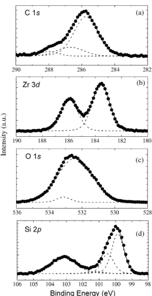
Fig. 2. XPS spectra showing the measured data in filled circles and fitted peaks in dotted lines for as-deposited Zr silicate film with 12 cycles at 550 8C. (a) C 1s spectrum, (b) Zr 3d spectrum with two peaks at 183.59 and 185.99 eV, (c) O 1s spectrum with two peaks at 532.45 and 533.15 eV, and (d) Si 2p spectrum with four peaks at 99.9, 100.51, 101.26, and 103.20 eV.
microscopy (AFM) and medium energy ion scattering (MEIS) and the details of these studies and the electrical properties are reported elsewhere w2x.
3. Results and discussion
Fig. 1a and b show the cross-sectional HRTEM images of sample 3 and 5, respectively. NO gas was used as an oxidant for both samples to intentionally grow the oxynitride layer. The Zr silicate film was deposited with O for sample 3 and NO for sample 5.2 The thicknesses of the silicate layers are about the same (approx. 1.1 nm) since both are deposited with the same deposition cycle number. However, the sample 5 has much thinner interfacial layer than the sample 3, indi-cating that using NO during the deposition of top layer is effective in retarding the further growth of interfacial layer. The results of HRTEM measurement for other samples are listed in Table 1. In all cases, the Zr silicate layer and the interfacial layers were observed to be amorphous.
The XPS of C 1s in Fig. 2a shows the existence of the carbon contamination due to residuals from the precursors and the ambient contamination during transfer to XPS system. After two cycles of sputtering, the peaks disappeared, indicating the bulk carbon concentrations were below the limit of our experimental instrument (-0.1 at.%). Therefore, the ultrathin surface layer contain-ing carbon assumed in the medium energy ion scattercontain-ing (MEIS) analysis was not included in the structure model of SE w2x. The Zr 3d spectrum in Fig. 2b consists of a doublet with peaks at 183.59 and 185.99 eV, which can be ascribed to Si–O–Zr bonds. There is no evidence of Zr–C or Zr–Si bonds as well as Zr–Si species associated with ZrSi phase in this spectrum, indicating that oxi-2 dation of Si substrate in either NO or O gas before the2 deposition of Zr silicate may prevent the possible for-mation of zirconium silicide in the interfacial layer. Meanwhile, the zirconium silicide film was observed for a zirconia film grown on HF last Si w3,4x. The O 1s spectrum in Fig. 2c shows two peaks at 532.45 and
Fig. 3. (a) The measured SE data compared with the best fitting for sample 1. The solid lines are measured data at 60 and 758 of angle of incidence and the symbols are reconstructed data obtained by using the best fitting parameters. (b) A plot of film thickness of interfacial layer vs. the deposition cycle numbers. Two square symbols for sam-ple 5 shows the non-uniformity of the ultrathin interfacial layer.
related with the oxynitride layer underneath the silicate layer. The binding energy difference E (O 1s)yE (Zrb b 3d5y2)s348.86 eV and E (O 1s)yE (Si 2p)s429.25b b eV are very close to the reported values of Zr-silicate of 348.35 and 429.5 eV w5x.
For SE, the best fitting of the parameterized model to the measured data is obtained by minimizing an unbiased test function using the Levenberg–Marquardt algorithm. The layer structure model consisted of sub-strateyinterfacial layeryZr silicateyambient is used to determine the film thickness and the optical constants of interfacial layer of each sample. The model also includes 2.5 A-thick rough surface measured by the˚ separate AFM measurement wnot shownx. The rough surface is assumed to be the equal mixture of Zr silicate and the void by using the Bruggeman effective medium approximation (BEMA). The roughness of the interfa-cial layer boundary was not included in our layer model. For ultrathin layers, the accurate determination of each parameter is a difficult matter because of the correlation between the fitting parameters. Since we are interested in studying the optical properties of the interface, we fixed the thickness and the composition of the Zr silicate layer according to the results of HRTEM and MEIS, respectively. In our previous MEIS analysis, the as-deposited Zr silicate layer is found to be ‘amor-phous’ with a Si:Zr ratio of 1.3:1, which is very close to the initial mixture ratio, 1.2:1 for the precursors w55% of Si(O -B u) (thd) : 45% of Zr(O -Pr) (thd) x. Also,t i
2 2 2 2
this ratio is used as the mixture ratio of SiO and ZrO2 2 in the structure model of SE analysis to simulate the Zr silicate films w2x. The fixed optical constants of SiO ,2 ZrO , w6x and bulk Si w7x from the literatures are used2 in the model. The band gap of crystalline SiO is ;92 eV, while that of crystalline ZrO is ;5.1 eV. Therefore,2 we expect the silicate to have a band gap somewhere in between these limits. Since the spectral range for our ellipsometer is limited between 1.33 and 4.7 eV, the imaginary part of dielectric function is assumed to be close to zero for Zr silicate layer. Then, both the thickness of interfacial layer and the mixture ratio of composition of each sample were chosen to be the fitting parameters in SE.
According to XPS measurement of the sample 5 in Fig. 2d, Si 2p spectrum shows peaks at 101.26 and 103.20 eV. The peak at 101.26 eV is due to an intermediate oxidation state since the peak appeared between Si2q (approx. 101 eV) and Siq3 (approx. 102 eV) shows the peak position of SiO and the peak atx 103.20 eV which is 3.3 eV away from the Si substrate peak at 99.9 eV corresponds to that of SiO w8x. This is2 a characteristic of Zr silicate but also could be due to the incomplete oxidation of a silicon oxide interfacial layer. Therefore, we used SiO mixed with SiO through2
the BEMA to simulate the composition of materials in the interfacial layer in SE study. We found that modeling the interfacial layer as a region of pure SiO w9x or mixing of crystalline Si w10x or amorphous Si with SiO w11x did not improve the fitting. Also, assuming2 that the interfacial layer is transparent and has a disper-sion similar to SiO w9x could not provide a good fitting2 to the data at higher energy range ()4 eV). Including non-zero imaginary dielectric function for interfacial layer is essential to fit the experimental data, especially for simultaneous fitting of data measured at multiple angles of incidence. Within this thin interface, assuming the interface with grading index profile was turned out to be very difficult and also did not improve the fitting at all. Therefore, all interface layers are assumed to be homogeneous, isotropic layers with sharp boundaries.
Fig. 3a shows the ellipsometrically measured data for sample 1 at the incident angle of 60 and 758 compared with the best fitting. The symbols are measured data and the solid lines are reconstructed data with the best fitting parameters in the structure model described above and they show the excellent consistency. The visual comparisons for other samples are almost identical. The comparison of thickness obtained from SE and HRTEM for each sample and the atomic fraction of interfacial layers is listed in Table 1, where the fitting residuals
is the goodness-of-fit parameter. The thickness of inter-facial layers obtained from SE show the excellent agreement with those from HRTEM. Here, the expanded uncertainty of our SE is ;0.3 nm while the HRTEM has the thickness determination error of ;0.4 nm.
The ellipsometrically determined thickness of inter-facial layers vs. deposition cycle numbers are plotted in Fig. 3b. Regardless the choice of oxidation gas and the
number of deposition cycles, the interfacial layer thick-ness for each sample except sample 5 is nearly the same (approx. 2 nm) within the accuracy error of SE. For samples 1–3, the use of NO gas as oxidant was not effective in substantial reduction of the interfacial layer thickness. The same was observed for hafnium silicate films grown by using the amide precursors, w(C H )2 5 2 Nx Hf and w(CH ) Nx Si w12x. For samples 1 and 24 3 2 4 with 21 and 30 cycle numbers, respectively, this may be due to that more oxygen incorporates with the substrate during the longer exposure of the wafer to the oxygen-based precursors. For these samples, however, the thickness of interfacial layer did not proportionally grow thicker as the top silicate layer increased, suggest-ing the oxidation process may be self-limited as observed for ultrathin zirconia films grown by room temperature UV-ozone oxidation w13x. Thicker interfa-cial layer for sample 3 than 5 is attributed to the choice of the gas wO x during the deposition of silicate film.2 For sample 4, using O for both oxidization and depo-2 sition caused the increase of top silicate layer as well as interfacial layer.
Despite the thickness of the interfacial layer for sample 5 varied within 0.6–1.5 nm because of the film non-uniformity, it was considerably thinner than that of other samples. It demonstrates that a carefully designed growth condition during the low pressure MOCVD with oxygen-based precursors can substantially reduce the growth of interfacial layer. However, any source of oxygen in the growth chamber may induce the signifi-cant incorporation of the oxygen with the substrate and consequently thicker interfacial layer. The spike anneal-ing of as-deposited sample 5 in O at 850 8C for 60 s2 shows the dramatic increase of interfacial layer, while the thickness of the Zr silicate top layer remains unchan-ged w2x. This may indicate that oxygen or residual water vapor in the thermal processor diffuses through the Zr layer to the silicon interface during the spike annealing. To confirm our result on the composition of the interfacial layer, we also have tried an oxynitride-like interfacial layer in SE analysis. It improved the final fitting (smaller correlation coefficient), but evidently underestimated the interface thickness as shown in Table 1. The discrepancy in thickness with TEM results is as big as 0.5 nm. Only sample 5 shows a close value to TEM result, confirming that the interfacial layer for this sample is mainly composed of the oxynitride film. Our previous study of other samples using MEIS revealed that the concentration of the nitrogen in the interfacial layer is 3.3=1014 nitrogen atomycm , approximately a2 half-monolayer of Si atoms on Si(100) and, therefore negligible w2x.
4. Conclusion
In this paper, we demonstrated that ultrathin Zr silicate films can be successfully deposited on Si(100) by using Zr(O -Pr) (thd) and Si(O -B u) (thd) as precursors ini t
2 2 2 2
a pulse-mode MOCVD. We studied the role of ambient gas on the formation of the interfacial layers during the oxidation and the deposition of ultrathin Zr silicate films using multiple analysis methods.
We found that pre-oxidation of the substrate in NO can effectively reduce the formation of thick oxide interfacial layer only under the very limited growth condition. Any source of oxygen in the growth chamber can cause the significant growth of the interfacial layer. However, the interfacial layer thickness is self-limited to approximately 2 nm under the several different growth conditions. No evidence of C–Si, Zr–Si, and Zr–C bonds was found in the XPS spectra and the concentrations of nitrogen and Zr in the interfacial layer were below the sensitivity of our facility. Variable-angle SE successfully analyzed the ultrathin interfacial layers as the amorphous mixture of SiO2 and SiO. The comparison of the interfacial layer thickness between HRTEM and SE shows an excellent consistency. Modeling of the inter-facial layers composed of oxynitride in SE underesti-mates the thicknesses of the interfacial layers, except the one with the reduced, thin interfacial layer grown with NO gas.
References
w1x G.D. Wilk, R.M. Wallace, J.M. Anthony, Appl. Phys. Rev. 89 (2001) 5243.
w2x H.-W. Chen, T.-Y. Huang, D. Landheer, X. Wu, S. Moisa, G.I. Sproule, J.-K. Kim, W.N. Lennard, T.-S. Chao, J. Electrochem. Soc. 150 (2003) C465.
w3x (a) Y.M. Sun, J. Lozano, H. Ho, H.J. Park, S. Veldman, J.M. White, Appl. Surf. Sci. 161 (2000) 115
(b) G.D. Wilk, R.M. Wallace, Appl. Phys. Lett. 76 (2000) 112.
w4x S. Ramanathan, P. Mcintyre, Appl. Phys. Lett. 80 (2002) 3793. w5x J. Guittet, J.P. crocombette, M. Gautier-Soyer, Phys. Rev. B63
(2001) 125 117.
w6x E.D. Palik (Ed.), Handbook of Optical Constants of Solids, Academic, Boston, 1991.
w7x G.E. Jellison Jr, Opt. Mater. 1 (1992) 41. w8x K. Muraoka, Appl. Phys. Lett. 80 (2002) 4516.
w9x C.M. Herzinger, B. Johs, W.A. McGahan, J.A. Woollam, J. Appl. Phys. 83 (1998) 3323.
w10x (a) V.A. Yakovlev, E.A. Irene, J. Electrochem. Soc. 139 (1992) 1450
(b) V.A. Yakovlev, Q. Liu, E.A. Irene, J. Vac. Sci. Technol. A10 (1992) 427.
w11x (a) D.E. Aspenes, J.B. Theeten, Phys. Rev. Lett. 43 (1979) 1046
(b) D.E. Aspenes, J.B. Theeten, J. Electrochem. Soc. 127 (1980) 1359.
w12x D. Landheer, X. Wu, H.-W. Chen, M.S. Lee, S. Moisa, T.-Y. Huang, T.-S. Chao, S.-H. Lu, W.N. Lennard, Proceedings of 2002 2nd meeting of the Electrochemical Society, Salt Lake City, USA, October 20–25, 2002, abstract 382.