HAL Id: hal-01239444
https://hal.archives-ouvertes.fr/hal-01239444
Submitted on 7 Dec 2015
HAL is a multi-disciplinary open access archive for the deposit and dissemination of sci-entific research documents, whether they are pub-lished or not. The documents may come from teaching and research institutions in France or abroad, or from public or private research centers.
L’archive ouverte pluridisciplinaire HAL, est destinée au dépôt et à la diffusion de documents scientifiques de niveau recherche, publiés ou non, émanant des établissements d’enseignement et de recherche français ou étrangers, des laboratoires publics ou privés.
Dynamic system level ESD current measurement using
magnetic field probe
Fabrice Caignet, Nicolas Nolhier, Marise Bafleur
To cite this version:
Fabrice Caignet, Nicolas Nolhier, Marise Bafleur. Dynamic system level ESD current measurement using magnetic field probe. Asia-Pacific International Symposium on Electromagnetic Compatibility ( APEMC ), May 2015, Taipei, Taiwan. �10.1109/APEMC.2015.7175400�. �hal-01239444�
Dynamic System Level ESD Current Measurement
Using Magnetic Field Probe
Fabrice Caignet #1, Nicolas Nolhier #2, Marise Bafleur #3
#CNRS, LAAS, 7 avenue du colonel Roche, F-31400 Toulouse, France +Univ de Toulouse, UPS : F-31400, Toulouse, France
1[email protected] 2nolhier@laas. 3bafleur@laas.
Abstract— Nowadays, embedded systems are playing an
important role thanks to the increased performance of the integrated circuits (IC). ElectroStatic Discharges (ESD) at system level regarding their impact at IC level is not well defined. With the evolution on semi-conductor manufacturer requirements, ICs robustness becomes an important concern since more and more functionalities of a product are embedded into a single chip. One of the main problems to understand system level is to identify the propagation of an ESD stress within the system and to extract the precise resulting waveform and its impact on the IC. Characterization methods to understand the interaction between the IC and the rest of the system are missing. In this paper we present how to use a magnetic field probe for dynamic measurement of the current propagation at system level. The calibration procedure is presented, and comparison with measurements shows the accuracy of the probe for system level ESD measurement. Using this technique, a cartography procedure enables the realization of movies showing the propagation of the ESD stress within the system.
I. INTRODUCTION
With the steady increase in the performance of integrated circuits driven by the shrinking of transistor dimensions, electronic systems are becoming more and more widespread. Therefore, system level design to preserve reliability against transient phenomena such as electrostatic discharges (ESD) is a challenging issue. The ESD requirements become even more severe as well as the emergence of applications directly exposing specific IC pins to the outside world. As a result, the demand for robustness against system-level, defined by IEC61000-4-2 standard [1], is increasingly shifted to the IC component itself [2] [3]. Therefore, taking into account these disturbances during the system design phase becomes necessary to improve the system immunity. To implement such predictive approach, both modeling and characterization methodologies should be developed and concurrently, precise measurement technique to compute current path on the system have to be set up.
In this work, we propose a non-invasive measurement technique for current monitoring at printed circuit board
(PCB) level. The technique is based on the use of a magnetic field probe. Such equivalent measurement technique has been presented in [4] and[5]in a similar way. Now this technique is used at LAAS-CNRS to analyze how current propagates into the system. The paper will describe how we build up this probe and how we calibrate it based on the simple consideration that the coupling between the PCB tracks and the probe is purely inductive. This consideration will be explained as well as the way to reconstruct the waveform of the current though the PCB. The calibration structure of the probe will be given and precise comparison between a 1 ohm measurement will be exposed to validate the accuracy of the measurement. This case of study is directly extracted from previous publication where the current path into a device where modified by a decoupling capacitance [6]. Finally using such current computation technique we present how from cartography of the board we build a movie showing how the ESD current propagates into the system depending on its configuration.
II. MAGNETIC FIELD PROBE FOR CURRENT MEASUREMENT
The probe (Fig. 1a) used to get the magnetic field emission while the current propagates is the same as the one used in the EMC standard [7].
fig.1 : (a) Home-made magnetic field probe. (b) Equivalent model of the probe.
The probe is made from a semi-rigid copper coaxial cable. The inner conductor of the coaxial cable is twisted and shorted to the outer shield, thus creating a current
loop. As shown in Fig. 1b, to model the probe, we use an inductance and a capacitor to represent the loop and a transmission line to take into account the RG402 high frequency coaxial cable used.
The equivalent transmission coefficient, S12, of the probe with the 50Ω adapted line is reported in Fig. 2, and clearly shows the pure magnetic coupling effect up to 1 GHz. Regarding the S12 coefficient, the transmitted power depends on the frequency and up to 1GHz the main coupling effect is the inductive one. The di/dt of the stress on the line induces a purely inductive noise on the probe following the equation:
€ Vind = k di dt and
€ k = M L1L2
Where M is the mutual coefficient, L1 and L2 the inductance of the probe and the line 50Ω.
Taking into account this coupling model a mutual coefficient, M, of 0.03 nH can be used with sufficient accuracy between probe inductance and line inductance when the probe is placed at 500 µm above a PCB line.
-60 -50 -40 -30 -20 -10 0 10# 100# 1000# +20dB/dec Frequency (MHz) S1 2 (d B ) Inductive model Measurement of magnetic probe
Fig. 2. S12 coefficient of the coupling probe and a 50Ω adapted line versus frequency.
This injection model has already been used in previous works [8]-[9] and various experiments are made to validate the probe model. Further information on this probe model and the set-up used to measure the transmission coefficient between the probe and a 50-Ω adapted line is available in [10]. Based on the consideration that the probe is purely inductive up to 1GHz, we directly reconstruct the waveform of the current through the PCB line by making an integration of the measured magnetic field.
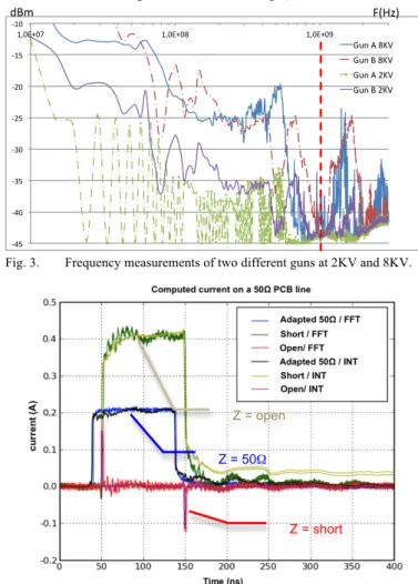
But with regard to ESD stresses, we have to validate that 1GHz probe bandwidth is enough to reconstruct the dynamic behavior of the current. Some frequency measurements of guns from two different manufacturers have been performed with stresses of 2KV and 8KV
(Fig. 3). The two guns exhibit very different spectral response. For 2KV injection, the signal amplitude for frequencies higher than 1Ghz is negligible. For 8KV (35A pick) stresses, a resonance is observed around 1.5GHz. Related to this observation, we can conclude that a 1 GHz probe bandwidth could be enough for lower amplitude, and integral reconstruction waveform can be used. For high voltage discharges, we need to work in the frequency domain (perform FFT of the dynamic measurement from the probe, make correction with the frequency response of the probe and finally make an FFT-1 to get the current shape).
!45$ !40$ !35$ !30$ !25$ !20$ !15$ !10$
1,0E+07$ 1,0E+08$ 1,0E+09$
Gun$A$8KV$ Gun$B$8KV$ Gun$A$2KV$ Gun$B$2KV$
dBm$ F(Hz)$
Fig. 3. Frequency measurements of two different guns at 2KV and 8KV.
Fig. 4. Calibration of the coupling probe on a 50Ω adapted line versus terminal impedance (50Ω, open and short).
This have been validated on a calibration structure make up of a 50 Ω line with 50Ω termination, shortcut and open-port, respectively. The injection is performed using a square pulse from VF-TLP with 300ps rise time and 100ns duration. Figure 4 shows the obtained results after a simple mathematical calculation using integral method (noted INT) and into the frequency domain (noted FFT). The measurements confirm the accuracy of the probe up to 1GHz and reveals the influence of the
Z = short
Z = open Z = 50Ω
termination. The frequency computation exhibits a higher dynamic than the integral computation method.
III. VALIDATION ON A SIMPLE CASE OF STUDY
For validation, the magnetic field measurement is directly used on a simple example where the impact of a decoupling capacitance on the current propagation is studied [11]. The paper presents the measurement of the current going out of an inverter by applying a 1A, 100ns square pulse using a VF-TLP tester. The measurement was obtained by using a 1Ω resistance. The injection is performed on one output of the IC and we measure the current going out of the chip through the ground pin (fig 5). In figure 6, the computed measurement obtained by the field probe is compared to the 1Ω measurement. The external decoupling capacitance placed on VDD pin dramatically changes the shape of the injected square pulse.
Decoupling Capacitance 110Ω line
Field probe
figure 5 : Schematic diagram of the test setup to get the currents going out of a chip using 1Ω resistance and field measurement.
Fig. 6. Current measurement from a 1A, 100ns pulse on the Vss pad of an inverter using 1Ω resistance and magnetic field probe.
It can be noticed that the reconstructed shape from the magnetic field probe is good enough to clearly exhibit that the ESD current going through the ground is not the expected one. The measurement we obtain shows some discrepancies that should be related to the fact that there is a via close to our measurement point, which could
introduce some variations in the magnetic field collected by the loop, and the dynamic aspect is reproduced.
Thanks to this validation, and to understand how the current can propagate on a system at board level, we developed an ESD scanning system as reproduced in figure 7.
Figure 7 : Setup of the ESD scanning system.
The field probe is mounted on a 3D axis system with a maximum spatial resolution of 100µm. The TLP generator synchronizes the measurement test bench. Each time a stress is injected into the connector of the PCB, HX and HY fields are captured using a 6GHz
oscilloscope. By repeating this operation the scan of the system is performed. From the registered data, a movie can be built showing the evolution of the emitting field during an electrical fast transient. Figure 8 (a) reports three pictures from the system of fig. 5 at different times. The integral computation of the magnetic field gives the current propagation into the system as reported in figure 8 (b).
Echan&llon)515) Echan&llon)563) Echan&llon)572)
Capa
IC 1 ohm Out
(a)
Current'injec+on' Decoupling'capacitance'absorp+on' Current'spleet'into'the'capa'And'the'1'ohm'resistance''
Capa
IC Out 1 ohm
(b)
Figure 8 : Picture from the magnetic field’s movie (a) and from the movie of the current propagation into the board (b). TLP stress injection (1ns rise time -100ns duration).
Direct measurement of the field probe
1Ω measurement
integral of the field probe measurement
Voltage (V)
Using such test equipment we are able to acquire the current during its propagation into the system. The waveform obtained in figure 6 with a square stress cannot be predicted by the ESD strategy of the chip. The current propagates into the chip and goes out through the power decoupling capacitance. The scanning system allows a dynamic measurement of the impact of all the elements implemented into the system. It is a powerful tool for system level ESD investigation used into current projects to understand the behavior under different types of ESD stresses.
IV. CONCLUSION
In this paper, we have investigated the possibility of using a magnetic field probe for the measurement of ESD currents on system level consideration. Our study was motivated by the difficulty to obtain the current shape on any point of a PCB without developing a dedicated PCB or inserting common probes that modify the impedances and as the consequence, the response of the system itself. Moreover, depending on the elements of the PCB (lines, passives, and ICs behavior) it is extremely difficult to predict the propagation of the stress into the system and so the failures. We demonstrated that radiated modes generated by the current propagation of an ESD stress are in the range of the frequency response of the probe. By using mathematical computation (integral method of frequency method) it is possible to reconstruct the shape of the current on the above PCB lines. We have presented some measurements from the characterization of the probe, and one comparison on a real case of study that resulted with the same shape as the one obtained through a resistance. By using a scanning system the dynamic propagation of the stress on the PCB structure can be accurately reproduced. This measurement system
is a powerful investigation tool that helps visualize how a system responses to an electrical stress.
REFERENCES
[1] IEC61000-4-2. Electromagnetic Compatibility. Electrostatic discharge immunity test – Basic EMC Publication. 1995.
[2] M. P. J. Mergens, M. T. Mayerhofer, J. A. Willemen, M. Stecher, ESD Protection Considerations in Advanced High-Voltage Technologies for Automotive, EOS/ESD Symposium, 2006, pp.54-63.
[3] T. Smedes, J. Van Zwol, G. De Raad, T. Brodbeck, H. Wolf,Relations Between System Level ESD and (vf-) TLP, EOS/ESD Symposium, 2006, pp.136-143.
[4] F.CAIGNET, N.MONNEREAU, N.NOLHIER, « Non-invasive system level ESD current measurement using magnetic field probe », International Electrostatic Discharge Workshop 2010, Tutzing (Allemagne), 10-13 Mai 2010
[5] Wei Huang et al., “Probe characterization and data process for the current reconstitution by near field scan method,” IEEE International Symposium of Electromagnetic Compatibility, 2010.
[6] N. Monnereau, F. Caignet, D. Tremouilles et al. « Building-up of system level ESD modeling: Impact of a decoupling capacitance on ESD propagation », Microelectronics Reliability Volume: 53 Issue: 2 Pages: 221-228, FEB 2013.
[7] IEC 61967-3: “Integrated Circuits, Measurement of Electromagnetic Emissions, 150 kHz to 1 GHz – Part 3 : Measurement of Radiated Emissions – Surface Scan Method”.
[8] N. Lacrampe, A. Boyer, B. Vrignon, N. Nolhier, F. Caignet and M. Bafleur, "Investigation of the indirect effects of a VF-TLP ESD pulse injected into a printed circuit board," in Workshops of International Symposium on Electromagnetic Compatibility, Immunity at the IC level, EMC Europe, Barcelona, Spain, September 2006, pp. 538-545. [9] N. Lacrampe, A. Boyer, N. Nolhier, F. Caignet and M. Bafleur,
"Original methodology for integrated circuit ESD immunity combining VF-TLP and near field scan testing," in Proceedings of the 3rd EOS/ESD/EMI Workshop, Toulouse, France, May 2006, pp. 51-54. [10] A. Boyer, S. Bendhia, E. Sicard, “Characterization of Electromagnetic
Susceptibility of Integrated Circuits using Near-Field Scan”, in Electronic Letters, Vol. 43, no. 1, pp 15-16, 4th January 2007. [11] Monnereau, N.; Caignet, F.; Tremouilles, D.; et al. « Building-up of
system level ESD modeling: Impact of a decoupling capacitance on ESD propagation », Microelectronics Reliability Volume: 53 Issue: 2 Pages: 221-228, FEB 2013.