HAL Id: hal-01407911
https://hal.archives-ouvertes.fr/hal-01407911
Submitted on 2 Dec 2016
HAL is a multi-disciplinary open access
archive for the deposit and dissemination of
sci-entific research documents, whether they are
pub-lished or not. The documents may come from
teaching and research institutions in France or
abroad, or from public or private research centers.
L’archive ouverte pluridisciplinaire HAL, est
destinée au dépôt et à la diffusion de documents
scientifiques de niveau recherche, publiés ou non,
émanant des établissements d’enseignement et de
recherche français ou étrangers, des laboratoires
publics ou privés.
Mixed monolithic-hybrid integration of multiphase
power converter: preliminary evaluation of the 3-chip
integration concept
Adem Lale, Nicolas Videau, Abdelhakim Bourennane, Frédéric Richardeau,
Samuel Charlot
To cite this version:
Adem Lale, Nicolas Videau, Abdelhakim Bourennane, Frédéric Richardeau, Samuel Charlot. Mixed
monolithic-hybrid integration of multiphase power converter: preliminary evaluation of the 3-chip
integration concept. ESARS ITEC 2016 - 4th International Conference on Electrical Systems for
Aircraft, Railway, Ship propulsion and Road Vehicles & International Transportation Electrification
Conference, Nov 2016, Toulouse, France. �hal-01407911�
Mixed monolithic-hybrid integration of multiphase
power converter: preliminary evaluation of the 3-chip
integration concept
Adem Lale
(1), Nicolas Videau
(1,2,3), Abdelhakim Bourennane
(1), Frédéric Richardeau
(2,3), Samuel Charlot
(1) (1) LAAS-CNRS, University of Toulouse, CNRS, UPS, Toulouse, France(2) University of Toulouse; INP, UPS; LAPLACE (Laboratoire Plasma et Conversion d'Energie) ENSEEIHT, 2 rue Charles Camichel, BP 7122, F-31071 Toulouse cedex 7, France - (3) CNRS; LAPLACE; F-31071 Toulouse
Abstract — The authors present a 3-chip mixed integration
approach that combines monolithic silicon multi-terminal power chips and flip-chip assembly on a printed circuit board (PCB) for the realization of a multiphase power converter. The overall approach allows for taking advantage of the degrees of freedom offered by silicon and PCB technologies with a limited and well-mastered complexity. The multiphase converter is integrated within three multi-terminal chips that are judiciously packaged, using the partial flip-chip, on a PCB board so as to reduce the switching cell stray inductance as well as the impact of voltage variations on the common mode current that flows through the converter’s PCB. Using Si and SiC dipole MOSFET and diode chips, converters based on the 3-chip approach were realized and compared to the conventional one. The obtained commutation loop inductance value is reduced by at least a factor of two as compared to that of the conventional one.
Keywords— Buck converter, full bridge converter, orthogonal switching cell, parasitic inductance, monolithic intgration, reverse conducting IGBT, IGBT, diode.
I. INTRODUCTION
Currently commercialized conventional power modules are generally realized using 2D hybrid packaging technology in which two-terminal power dies such as Insulated Gate Bipolar Transistor (IGBT) and PiN-diode are bonded on their backside and interconnected using wire bonds. A power module is made of a great number of two-terminal dies that are interconnected by wire bonds. Power modules are therefore bulky and their mass fabrication is limited in productivity. Moreover, due to the fact that the power dies are soldered on their backside, the midpoints of the converter’s phase legs are placed on the circuit board. As a result, the circuit board is directly subjected to voltage variations during switching phases which is source of the undesirable common mode current through the circuit board. Moreover, wire bonds in power modules are source of parasitic inductance [1-2] that induces high turn-off voltage overshoot, which not only add electrical stress on the power dies, but also result in switching losses and thus affect the overall efficiency.
To improve reliability, electrical performance and reduce cost of power modules, significant breakthrough can be achieved by the monolithic integration of the 2D-multiphase module within a minimum number of multi-terminal dies that are judiciously packaged. Within the context of integration and
miniaturization, the reverse conducting Insulated Gate Bipolar Transistor (RC-IGBT), as described in Fig. 1(a) and (b), is considered as the elementary brick for converter integration. The RC-IGBT monolithically integrates an IGBT and an anti-parallel freewheeling PiN diode. The structure of the RC-IGBT was extensively studied in literature [3-4]. Using this device, the authors have recently proposed a vertical quasi-monolithic integration of power converter called two-chip approach as well as an ultra-compact single chip approach [5] aiming at reducing fabrication costs, improving electrical performance and reliability. Different approaches for converter integration were described in literature in order to reach similar objectives. However, they are either limited in performance (lateral integration with vertical insulation trenches [6]) or require a complex technological process for their realization (molecular bonding of two wafers [7]). The initial objective of the dual-chip integration[8] approach was to integrate the high-side part of the power converter within a single multi-terminal power chip named a “common anode” chip and the low-side part within another multi-terminal power chip named “common cathode” power chip as illustrated in Fig. 2(a). Each power chip is composed of a great number of quasi-parallel connected RC-IGBTs that share the same N- drift region as shown in Fig. 2b). The number of RC-IGBTs within each chip depends on the number of converter phases. Within the common cathode chip, each RC-IGBT section must be electrically insulated from the neighbouring RC-IGBT sections as illustrated in Fig. 3c). To that end, a vertical P+ wall that crosses vertically the silicon wafer and surrounds entirely each RC-IGBT section is used. However, the technological realization of the P+ wall is
clearly complex and an intensive process development is in progress today. To overcome the necessity of using a P+ wall
insulation that crosses vertically and entirely the silicon wafer, the authors propose in this paper original three multi-terminal power chips. Moreover, it will be demonstrated that the judicious packaging of these three multi-terminal chips allows to obtain switching cells of identical quality as those obtained using the two terminal approach.
The paper is organized as follows: the first section presents the “three-chip” power converter integration approach, the second section focuses on the packaging of the three multi-terminal chips on a PCB, and the last section details the different characterization techniques employed to the estimation of the commutation loop stray inductance.
(a) (b)
Fig. 1. (a) IGBT with its anti-parallel freewheeling diode, (b) a schematic cross-sectional view of an RC-IGBT integrating monolithically an IGBT and a freewheeling diode.
(b)
(a) (c)
Fig. 2. (a) The dual-chip integration approach, cross-sectional view of the: (b) common anode terminal structure, (c) common cathode three-terminal structure [8].
II. PRINCIPLE OF THE THREE-CHIP INTEGRATION APPROACH As detailed in Fig. 3 (a), (b) and (c), the whole row of high side Reverse-Conducting Insulated Gate Bipolar Transistors (RC-IGBTs) is integrated within a single multi-terminal chip named “common anode” while the low-side RC-IGBTs row is integrated within two distinct monolithic multi-terminal power chips: the low-side insulated gate bipolar transistors are integrated within one single multi-terminal power chip while the low-side power PiN diodes are integrated within another multi-terminal power chip as shown in Fig. 4. This allows overcoming the technological complexity encountered for the realization of the P+ wall that crosses vertically the silicon
wafer within the common cathode chip [8] that makes its process of realization complex [9-10]. For the purpose of validating the operating modes of the different chips using 2D SentaurusTM simulations, dielectrically filled trenches were
used within the frame of this study.
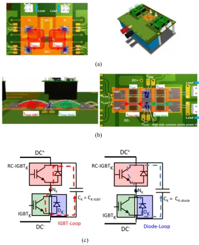
The optimized targeted packaging for the three-chip approach is shown in Fig. 3(b). The chips are packaged so that to minimize the length as well as the apparent surface of the commutation loops. So then, the unique high-side multi-terminal common anode chip is positioned at the centre and on its one side is placed the low-side multi-terminal IGBT power chip and on the opposite side the low-side multi-terminal diode power chip. In this way, as it is detailed in section §IV dedicated to packaging and characterization, the parasitic commutation loop inductance is reduced to that of a single set of wire bonds, instead of two series connected sets encountered in the case of conventional packaging. Moreover, the circuit board effect is reduced due to the fact that this latter is not directly subjected to dv/dt disturbances during switching phases. For buck and boost chopper applications, one of the low-side two multi-terminal chips becomes useless and the packaging can be reduced to only two multi-terminal power chips.
(a)
(b)
Fig. 3. (a) Principle of integrating a multiphase converter composed of K-phase legs using the 3-chip approach , (b) Schematic illustration of the 3-chip packaging.
(a)
(b) (c)
Fig. 4. 2D structures of the three-terminal chips for the case of an H-bridge inverter: (a) high-side common anode chip, (b) low-side multi-IGBT chip, (c) low-side multi-diode chip.
III. SENTAURUSTM MIXED-MODE SIMULATION RESULTS The main geometrical and physical parameters of the diffusion regions used in the IGBT and diode sections are those set by the IGBT process-flow of the micro and nanotechnology platform at LAAS-CNRS [8]. The drift region thickness is chosen so that the devices are able to withstand 600 V. In Fig. 5 and 6, the simulation conditions correspond to a static state: when one diagonal section of the bridge is in on-state the other is in off-on-state, a current source of 100 A/cm2
simulates an inductive load. The common anode concept was already validated in previous works of the authors [9] and is not described in this paper. In Fig. 5(a) and Fig. 6(a), 100A current flows through one section of each chip while the other
N-! P+ P P+ P N+ N+ N+ N+ Anode P+ N+ N+ P+ NP+ + Gate!
Cathode Cathode Gate! Gate! N+ Anode Cathode Gate VDC IGBT 1 IGBT 2 IGBT k D 1 D 2 D k N1 N2 Nk Common anode chip Mul9-diode chip RC-IGBT K RC-IGBT 2 RC-IGBT 1 Mul9-IGBT chip IGBT1 IGBT2 IGBTK RC-IGBT1 D1 D2 DK N1 N1 N2 N2 NK NK Low side mul0-IGBT Chip (composed of K IGBTs ) – flip chip High-side common anode mul0-terminal chip (composed of K RC-IGBTs) Low side mul0-diode Chip (composed of K PiN-diodes)
Anodes Cathodes Cathodes
Substrate
RC-IGBT2
section is in off-state (negligible leakage current). In Fig. 5(b) and Fig. 6(b), a 600V is supported by each section in off-state. Depletion regions (for reverse biased junctions) extend mainly into the lightly doped N- drift-region.
(a) (b)
Fig. 5. 2D mixed-mode SentaurusTM simulation results for the multi-IGBT
chip: (a) total current density, (b) equipotential lines.
(a) (b)
Fig. 6. 2D mixed-mode SentaurusTM simulation results for the multi-diode
chip: (a) total current density, (b) equipotential lines.
The multi-terminal chips were assembled to form a 3-chip inverter. A 600V DC supply is applied at the input and a 100A DC current supply simulate the load. The results obtained using mixed-mode SentaurusTM simulations are provided in figure 7.
Fig. 7. 2D Mixed-mode SentaurusTM simulation result for a two phase
inverter application.
IV. THREE-CHIP VERSUS REFERENCE ASSEMBLY A. Realized and characterized converter assemblies
The reference two-phase converter assembly makes use four Reverse Conducting-IGBTs. The targeted packaging for the full bridge converter circuit given in Fig. 8 (b), according to the proposed three-chip approach, is shown in Fig. 9 (d). The IGBTs chip (flipped) is positioned on one side (left-side in this case) of the common anode chip while the diodes chip is positioned on the other side (right-side in this case) of the common anode chip. Due to the fact that the realization of the proposed IGBT and diode Si multi-terminal chips is being in progress, the realized converter assemblies are buck type converters composed of fast two-terminal Si and SiC MOSFET dies as well as SiC diode dies (Table II) from commercial providers. These assemblies allow one to characterize the switching loop inductance.
(a) (b)
Fig. 8. Two-phase converters: (a) Reference using four RC-IGBTs , (b) According to the proposed 3-chip approach.
To evaluate the improvements brought by the proposed approach, generic layouts ere designed for the reference as well as 3-chip two-phase converters. Silicon as well as silicon carbide chips were used. As compared to Fig. 4, the RC1 and
RC2 of Fig. 9(c) form the common anode chip, IGBT1 and
IGBT2 form the multi-terminal IGBT-chip while D1 and D2 form the multi-terminal diode-chip. The optimized layout of the conventional converter results in a coplanar commutation loop of 130mm2 surface while the optimized 3-chip converter
leads to an orthogonal 3D-commutation loop of 26mm2 surface (ratio: 1/5).
(a)
(b)
(c)
Fig. 9. Layout of converter on the PCB board: (a) coplanar commutation loop for the reference assembly, (b) orthogonal commutation loop for the 3-chip, (c) illustration of the IGBT and diode power loops.
B. Switching loop modelling during low-side switch turn-off The use of a very small (negligible) gate resistance allows hard and fast turn-off switching. Consequently, the duration of Miller effect can then be neglected [12] and the switching cell can be modelled by the electrical circuit given in figure 10.
DC+ C1 RC-IGBT1 DC- N1 C2 RC-IGBT2 N2 CHV RC-IGBT3 RC-IGBT4 C1 IGBT1 D1 RC-IGBT1 DC+ DC- N1 C2 IGBT2 D2 RC-IGBT2 N2 CHV CK = CK-IGBT IGBTK DK RC-IGBTK DC+ DC- NK IGBT-Loop CK = CK-diode IGBTK DK RC-IGBTK DC+ DC- NK Diode-Loop
(a) (b)
Fig. 10. (a) The switching cell model including parasitic elements and (b) its circuit model at turn-off.
From the equivalent circuit of the switching cell composed of medium and high frequency loops (Fig. 10b), the peak overvoltage across the power device (MOSFET in this case) at turn-off can be expressed as follows:
Eq. (1)
(a) (b) (c) (d)
The term (a) represents the transfer of energy stored in the busbar inductance LBeq to the decoupling ceramic capacitors
Cdec. Terms (b) and (d) represent the different effects of
commutation loop stray inductances: (b) gives back the transfer of energy stored in the inductance loop LSCeq to the Coss
capacitance of the device, while (d) represents the relation between the turn-off di/dt and the inductive over-voltage across the device. A detailed analysis shows that during the dv/dt sequence just before the over-voltage, the current loop flows through the Coss part and the transition capacitor of the diode.
Then, the equivalent current loop in series with de device is reduced by a factor K = CT/(CT+Coss). It should be noted that
the term (a) is predominant at medium frequencies (< 50 MHz) while (b) is predominant at high frequencies (> 50 MHz) due to low values of LSCeq compared with LBeq and of Coss compared
with Cdec. Moreover, it can be noted that due to the low value
of Coss for fast WBG device such as Mosfet SiC, term (b) is
higher than term (d) by a ratio near to 20 (ex. numerical application: 5nH, 100pF, 1000A/µs, 30A, K = 0.5). Thus, it appears that the gate resistor and the channel control are not directly influent parameters to manage the HF phenomena. Parameters of the circuits such as stray inductances and capacitors values are clearly more influent on the over-voltage stress. Finally, term (c) easily reflects the forward dynamic recovery of the diode, mainly for Si-PiN diode that exhibits slow commutation behaviour in this work.
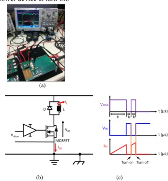
C. Double-pulse time-domain characterization of the switching loop
The used circuit is a buck-type converter composed of a high speed switching power device and a freewheeling diode. The operating principle consists in applying to the gate of the power device two consecutive short pulses. The first pulse is of duration (t1) relatively long allows the establishment of the load current, the second pulse of shorter duration (t3) and aims
at enabling the observation of oscillations in the output voltage waveform across the MOSFET at turn-off (figure 11(b)). The
stray inductance can then be deduced from the measurement of the oscillation frequency of the voltage waveform across the power device at turn-off.
(a)
(b) (c) Fig. 11. (a) test bench for electrical characterizations, (b) Electrical circuit in Buck-Type topology, (c) double short-pulse control signal.
The analysis of the components that compose the amplitude and oscillation-frequency, of the voltage waveform at turn-off, enables one to determine the parameters of the switching cell. From eq. (1), the High frequency term (HF) allows to determine the pair (LSCeq, Coss), medium frequency (MF) term
allows to characterize the pair (LBeq, Cdec). Conventional as
well as proposed 3-chip converters were realized using either Si-dies or SiC-dies and were characterized. The turn-off waveforms of Si and SiC assemblies, summarized in tables II and III, are provided in Fig. 12 and Fig. 13. The analytical expressions used to estimate the inductances values at medium and high frequencies are given in tables IV and V, respectively. Table IV is organized as follows: part (A) presents the medium-frequency (MF) measurements as well as calculations carried-out to estimate the busbar inductance (LBeq), part (B)
presents LBeq values obtained for the reference (classical) Si
and SiC assemblies, and part (C) presents LBeq values obtained
for Si and SiC assemblies based on the proposed 3-chip approach. Table V is organized as follows: part (A) describes high-frequency (HF) measurements as well as calculations carried-out to estimate the switching cell inductance (LSCeq),
part (B) presents LSCeq values obtained for the reference
(classical) Si and SiC assemblies, and part (C) presents LSCeq
values obtained for Si and SiC assemblies based on the proposed 3-chip approach.
t (µs) Vdrive t1 t2t3 t (µs) Vds t (µs) Ids
Amorçage BlocageTurn-on Turn-off
MOSFET L D VDS Vdrive IL IDS MOSFET Load D Vds Vgs CP load CP busbar Cdec ESL ESR LS Ld RLoad Vd0 LdA LdK LSC RSC Lbusbar Lbusbar Rbusbar Rbusbar VDC ILoad ILoad D Cdec ESL ESR RLoad Vd0 Rd LSCeq RSCeq Lbeq Rbeq VDC ILoad RdsON Ichannel = 0 C OSS High frequency loop (HF) medium frequency loop (MF) VCOSS
(
L ESL)
didt V C ESL L KI C L IVc diode SCeq channel
oss SCeq load dec Beq load ossMAX + + + + + = δ
TABLE I. DOUBLE-PULSE CHARACTERIZATION: SI AND SIC
“REFERENCE” CONVERTERS
Reference assembly
Using Silicon chips Using Silicon-carbide chips
Half-bridge
v Two Si-MOSFET (low-side + High-(low-side):
SIPC69N60C3
Buck-Type
v One SiC- MOSFET : CPM2-1200-0025B
+ v Three SBD SiC in
parallel : CPW4-1200-S015B
Half-bridge circuit (with stray inductances)
Gate drive voltage = +18V/-18V, External gate resistance Rg in the range
[0Ω, 10Ω]
Buck-Type circuit (with stray inductances)
Gate drive voltage =+19V/-2.5V, External gate resistance Rg in the range
[0Ω, 10Ω]
(a)
(b)
Fig. 12. Turn-off voltage waveforms for conventional (reference) (a) Si-converter assembly, (b) SiC Si-converter assembly.
TABLE II. DOUBLE-PULSE CHARACTERIZATION: SI AND SIC “PROPOSED”
CONVERTERS
Proposed assembly
Using Silicon chips Using Silicon-carbide chips
Buck-Type
v One Si- MOSFET: SIPC69N60C3 + v One diode: SIDC30D120H8 Buck-Type v One SiC-MOSFET: CPM2-1200-0025B +
v Two SBD SiC in parallel CPW4-1200-S015B
Buck-Type circuit (with stray inductances)
Gate drive voltage = +18V/-18V, External gate resistance Rg in the range
[0Ω, 10Ω]
Buck-Type circuit (with stray inductances)
Gate drive voltage =+19V/-2.5V, External gate resistance Rg in the range
[0Ω, 10Ω]
(a)
(b)
Fig. 13. Turn-off voltage waveforms for the proposed (a) Si-converter assembly, (b) SiC converter assembly.
11.7A% 0% Iload [5A/div] Vdsk Vd[20V/div] 0% Vsk[20V/div]
Time Base 400ns/div
2xδVdsk
1/FHF
Time Base 40ns/div
@RgExt.10Ω/100V-11.7A @RgExt. 0Ω/150V-26A
δVdsk HF = 6V FHF = 113.5MHz δVdsk MF = 1.6V FMF = 1.56MHz dV/dt = 6.3kV.µs-1% δVdsk HF = 24.5V FHF = 113.5MHz dV/dt = 24kV.µs-1% Zoom Vgs [10V/div] 0 Vdsk [20V/div] Vsupply [20V.div] Iload [5A/div] 0 RgExt. = 10Ω Vdrive +19V/-2.5V 0 0 Zoom 11.7A
Time base [400ns/div] Time base [40ns/div]
SK L Load VdsK VgsK LS DK RLoad LdA ILoad Rg Rg SK L Load D VdsK VgsK LS DK RLoad FWD (X3) LdA ILoad Rg L Load D RLoad FWD LdA I Load SK VdsK VgsK LS DK Rg VSK VDK L Load D RLoad FWD LdA I Load SK VdsK VgsK LS DK Rg VSK VDK
TABLE III. MEDIUM FREQUENCY STRAY INDUCTANCE VALUE:
MEASUREMENT AND CALCULATED (SEE (A),(B) AND (C) BELOW) A) Busbar characterization (Medium-Frequency loop) methods
(Equivalent localized physical quantities: Lbeq, Cdec)
Realized measurements Analytical expressions 1) Measurements using an impedance
analyzer, Agilent 4294A + dedicated PCB Probe 42941A
2) Time-domain measurements: carried-out using an oscilloscope TEK DPO4104B 1GHz/5GSamp.s-1 + Passive
voltage probes TPP1000 1GHz (Deskew mode + Hi/Average x4 mode)
From time-domain measurements, two techniques were used to calculate Lbeq:
Technique (a) From the voltage ripple (damping neglected --> giving a lower bound value):
Technique (b) From the oscillation period (damping neglected --> giving an upper bound value):
B) Busbar characterization (Medium-Frequency loop) : reference assembly
Type of Assembly Measurement using an
impedance analyzer Determined : Time-domain (Analytical) technique (a) Determined : technique (b)
Reference Si assembly (Type: Half-Bridge) Coss = 300 pF (at 100V) Coss = 220 pF (at 150V) --> K = 0.5 Cdec : 2xKEMETX7R -500V (measurements) 2x60 nF (at 100V) 2x45 nF (at 150V) ESL = 0.8 nH ESLeq = 0.4 nH Cfilter (fp) : EPCOS 2x3.3 uF/ 400V/ESLeqMAX= 9 nH Lbeq MEASURE = 10.03nH at 10MHz
“Short and wide” busbar Technique (a) 25A/100V/ Rg-10Ω/ δVCdec = 8.4V Technique (b) 25A/100V/ Rg-10Ω/3.8MHz Lbeq MIN = 13.5 nH Lbeq MAX = 14.6 nH Reference SiC assembly (Type: Buck) Coss = 470 pF (at 100V) CTdiode = 3x170 pF (at 100V) => K = 0.48 (at 100V) Technique (a) 11.7A/100V/ Rg- 10Ω/δVCdec = 3.4V Technique (b) 11.7A/100V/ Rg-10Ω/4.2MHz Lbeq MIN = 10.2 nH Lbeq MAX = 11.9 nH
C) Busbar characterization (Medium-Frequency loop) : proposed assembly Type of
Assembly Measurement using an impedance analyzer Determined Time-domain (Analytical) using technique(a) Determined using technique(b) Proposed Si (Type: Buck) Coss = 300pF (at 100V) CTdiode = 65pF (at 100V) => K = 0.82 (at 100V) Cdec : 6xKEMETX7R -500V (measurements) 6x60nF (at 100V) 6x45nF (at 150V) ESL = 0.8 nH ESLeq = 0.14 nH
Cfilter (fp) : EPCOS 2x3.3uF/
400V/ESLeqMAX= 9 nH
Lbeq MEASURE = 19.08nH@10MHz
"Long and narrow" busbar Technique (a) 10A/100V/ Rg 10Ω/δVCdec = 2V Technique (b) 10A/100V/ Rg10Ω/1.7M Hz Lbeq MIN = 14.4 nH Lbeq MAX = 24.3 nH Proposed SiC (Type: Buck) Coss = 470pF (at 100V) = 400pF (at 150V) CTdiode = 2x170pF (at 100V) = 2x140pF (at 150V) => K = 0.58 (at 100V) => K = 0.59 (at 150V) Technique (a) 24.5A/100V/ Rg.10Ω/ δVCdec = 5V Technique (b) 11.7A/100V/ Rg.10Ω/ 1.6MHz Lbeq MIN = 15.0 nH LbeqMAX = 27.5 nH
TABLE IV. HIGH FREQUENCY STRAY INDUCTANCE VALUE:
MEASUREMENT AND CALCULATED (SEE (A),(B) AND (C) BELOW) A) Switching-cell characterization (High-Frequency loop)
(Equivalent localized physical quantities: Lsceq, ESLdec, Coss)
Realized measurements Analytical expressions
1) Measurements using an impedance analyzer Agilent 4294A + dedicated PCB Probe 42941A 2) Time-domain measurements: carried-out using an oscilloscope TEK DPO4104B 1GHz/5GSamp.s-1
+ Passive voltage probes TPP1000 1GHz (Deskew mode + Hi/Average x4 mode)
From time-domain measurements, one can calculate Lsceq. Indeed, Lsceq can be
calculated by a combination of techniques (a) and (b) below. It can also be calculated using technique (c) below.
a) From the voltage ripple (damping neglected --> giving a lower bound value):
Buck-Type case: Half-Bridge case: b) From the voltage ripple given in "point (a)" and dVmax/dt
=>
c) From the oscillation period (damping neglectedà giving a upper bound value):
B) Switching-cell characterization (High-Frequency loop): reference assembly Type of Assembly Measurement
using an impedance analyzer Time-domain (analytical) Determined using techniques (a) + (b) Determined using technique (c) Reference Si assembly (Type: Half-Bridge) Coss = 300 pF (at 100V) Coss = 220 pF (at 150V) --> K = 0.5 9.5 nH (Extrapolated value) at 10MHz (4W in 2x series connected) a) 26A/100V/ Rg 0Ω/ δVCoss = 37V b) 25A/100V/Rg 10Ω/31.6kV.µs-1 c) 26A/100V/ 117MHz/ Rg 0Ω 28A/150V/ 133MHz/ Rg-0Ω => Lsceq MIN = 2.4 nH-4.4 nH 6.1 nH-6.5 nH => Lsceq MAX = Reference SiC assembly (Type: Buck) Coss = 470 pF (at 100V) CTdiode = 3x170 pF (at 100V) => K = 0.48 (at 100V) 10.7 nH at 10MHz (3W in 2x series connected) a) 11.7A/100V/ Rg 10Ω/δVCoss = 16V b) 11.7A/100V/ Rg10Ω/ 5.9kV.µs-1 c) 11.7A/100V/ 72.7MHz/ Rg-10Ω => Lsceq MIN = 3.8 nH-7.7 nH => Lsceq MAX = 10.2 nH )² . 2 .( 1 MF dec beqMAX F C L π = load eq Coss oss sceqMIN KI ESL V C L ⎟⎟ − ⎠ ⎞ ⎜ ⎜ ⎝ ⎛ = 2 . . δ 2 1 = K 2 . ⎟ ⎟ ⎠ ⎞ ⎜ ⎜ ⎝ ⎛ = load Cdec dec beqMIN C IV L δ ( ) eq load Coss sceqMIN KI VdV dt ESL L = − / . . max 2 δ dVmax dt = K.Iload Coss Tdiode oss oss C C C K + = )² . 2 .( 1 HF oss sceqMAX F C L π =
C) Switching-cell characterization (High-Frequency loop): proposed assembly Type of Assembly Measurement
using an impedance analyzer
Time-domain (Analytical) Determined using techniques (a)
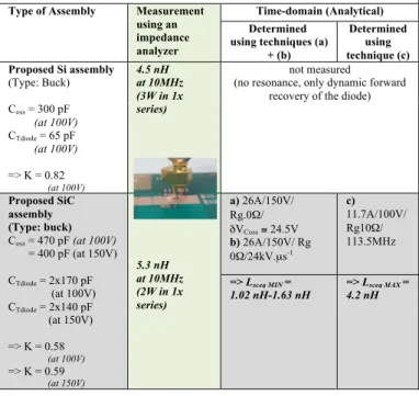
+ (b) Determined using technique (c) Proposed Si assembly (Type: Buck) Coss = 300 pF (at 100V) CTdiode = 65 pF (at 100V) => K = 0.82 (at 100V) 4.5 nH at 10MHz (3W in 1x series) not measured
(no resonance, only dynamic forward recovery of the diode)
Proposed SiC assembly (Type: buck) Coss = 470 pF (at 100V) = 400 pF (at 150V) CTdiode = 2x170 pF (at 100V) CTdiode = 2x140 pF (at 150V) => K = 0.58 (at 100V) => K = 0.59 (at 150V) 5.3 nH at 10MHz (2W in 1x series) a) 26A/150V/ Rg.0Ω/ δVCoss ≅ 24.5V b) 26A/150V/ Rg 0Ω/24kV.µs-1 c) 11.7A/100V/ Rg10Ω/ 113.5MHz => Lsceq MIN = 1.02 nH-1.63 nH => Lsceq MAX = 4.2 nH
D. Characterizations using an impedance analyzer
It uses an Agilent 4294A" (Fig. 14(a)) equipped with a sensor head "co-axial 42941A" for PCB with compensated probe measurement in open circuit and short circuit at the operating frequency. It allows a wide frequency range measurement up to 110 MHz of the switching loop impedance without placing the dies on the PCB. The values obtained by this technique were reproducible and were considered as reference values for comparison purposes. The optimized proposed 3-chip orthogonal switching cell presents a stray inductance which is lower than half that presented by the classical switching cell. The measured value for the proposed approach was about 4.5nH.
(a) (b)
Fig. 14. (a) Impedance measurement using an impedance analyzer, (b) case of classical switching cell.
V. CONCLUSION
Multi-terminal power dies suitable for the 3-chip integration approach of multi-phase power converter integration were proposed and validated by SentaurusTM 2D
simulations. A partial flip-chip packaging process was set-up. Converters assemblies composed of Si as well as SiC dies were realized and characterized for commutation loop stray inductance estimation. The switching cell inductance was determined from measurements using an impedance analyzer and also from time domain measurements using the double-pulse technique. A comparison between the value of the
switching loop inductance in the reference (classical) assembly and that in the proposed 3-chip assembly shows that a reduction by a factor of about two is obtained by the 3-chip approach (it is about 10.7 nH with the classical and about 4.5 nH with the proposed 3-chip approach). To reduce further the stray inductance value of the switching cell, the realization of a Direct Lead Bonding (DLB) version based on the proposed 3-chip assembly is in progress.
ACKNOWLEDGMENT
This research work received financial support from the French National Research Agency (ANR). The project name is "ConvPlUS", ANR-13-JS09-0008-01, using the technological support of RENATECH-LAAS and 3DPHI platforms.
REFERENCES
[1] S. Tanimoto and K. Matsui, “High junction temperature and low parasitic inductance power module technology for compact power conversion systems,” IEEE Trans. Electron Devices, vol. 62, no. 2, pp. 258–269, Feb. 2015.
[2] Shengnan Li; Tolbert, L.M.; Fei Wang; Fang Zheng Peng, "Stray Inductance Reduction of Commutation Loop in the P-cell and N-cell-Based IGBT Phase Leg Module", Power Electronics, IEEE Transactions on , vol.29, no.7, pp.3616-3624, July 2014.
[3] B. Yi, Z. Lin, and X. Chen, “Snapback-free reverse-conducting IGBT with low turnoff loss,” Electron. Lett., vol. 50, no. 9, pp. 703–705, Apr.2014.
[4] U. Vemulapati, N. Kaminski, D. Silber, L. Storasta, and M. Rahimo,“Reverse conducting–IGBTs initial snapback phenomenon and its analyticalmodelling,” IET Circuits, Devices Syst., vol. 8, no. 3, pp. 168-175, May 2014
[5] A. El Khadiry, A. Bourennane, F. Richardeau, E. Imberrnon, "New Monolithic Multi-poles Converter Device for Medium Power Applications", European Power Electronics Conference and Application, EPE-ECCE, Lappeenranta, Finland, 26 -28 août 2014. doi: 10.1109/EPE.2014.6911021.
[6] D.W Green, E.M Shankar Narayanan, "Fully Isolated High Side and Low Side LIGBTs in Junction Isolation Technology", Power Semiconductor Devices and IC's, ISPSD 2006. IEEE International Symposium on, pp.1-4, 2006.
[7] L. Benaissa et al., “A vertical power device conductive assembly at wafer level using direct bonding technology,” in Proc. IEEE 24th Int. Symp. Power Semiconductor Devices ICs , Jun. 2012, pp. 77–80 [8] E. Imbernon et al., "Flexible technological process for functional
integration" Int. Semicond. Conf. (CAS’2001) pp 65–68.
[9] A. El Khadiry, A. Bourennane and F. Richardeau, "Multiphase Power Converter Integration in Si: Dual-Chip and Ultimate Monolithic Integrations," in IEEE Transactions on Electron Devices, vol. 63, no. 5, pp. 1977-1983, May 2016.
[10] J.-L. Sanchez et al., “Realization of vertical P+ walls through-wafer for bi-directional current and voltage power integrated devices,” in Proc. IEEE 15th Int. Symp. Power Semiconductor Devices ICs (ISPSD), Apr. 2003, pp. 195–198.
[11] O. Causse, P. Austin, J.L. Sanchez, G. Bonnet and E. Scheid, "Achievement of a new peripheral planar structure supporting a symmetrical blocking voltage", 9th European Conference on Power Electronics and Applications (EPE'2001), Graz (Autriche), 27-29 Septembre 2001, 9p.
[12] T. Rossignol, F. Senghor, D. Risaletto, J.-M. Blaquière, F. Richardeau, M. Cousineau, “Switching optimization of WBG power devices on inverter leg “dv/dt – switching energy” trade off and comparison using directly the gate resistance or an additional feedback gate-drain capacitor”, PCIM Europe 2013, Nuremberg, 16 – 18 may 2013.