© Japanese Society of Electron Microscopy Journal of Electron Microscopy 48(6): 717-723 (1999)
Full-length paper
A comparison of HREM and weak beam
transmission electron microscopy for the
quantitative measurement of the thickness of
ferroelectric domain walls
HAFN Special Issue
M. Foeth*, A. Sfera, P. Stadelmann and P.-A. Buffat
Centre Interdepartemental de Microscopie Electronique, Bat. MXC-135, EPFL, CH-1015 Lausanne, Switzerland *To whom correspondence should be addressed. E-mail: [email protected]
Abstract In this paper we present two methods for the quantitative measurement of the thickness of ferroelectric domain walls, one using high-resolution electron microscopy (HREM) and the other weak beam transmission electron micro-scopy (WBTEM). These techniques can be used to determine the thickness of domain walls at room temperature as well as close to the ferroelectric to paraelectric phase transition. The first method allows a direct visualization of the lattice distortion across the domain wall, by measuring the continuous deviation of a set of planes with respect to the undistorted lattice. The second method consists in a quantitative analysis of the thickness fringes that appear on weak beam images of inclined domain walls. By fitting simulated fringe profiles to experimental ones, we can extract the thickness of the domain walls in a quantitative way. These two complementary techniques lead to a complete characterization of the thickness of ferroelectric domain walls over a wide range of specimen thicknesses at different magnifications. As an example we apply these methods to ferroelectric domain walls in PbTiO3.
The domain wall thickness at room temperature is found to be 1.5 ± 0.3 nm using HREM (in very thin samples =10 nm) and 2.1 ± 0.7 nm using WBTEM (in samples thicker than 30 nm).
Keywords high-resolution electron microscopy, weak beam imaging, ferroelectric domain walls, PbTiC^, image simulation, quantitative electron microscopy Received 11 December 1998, accepted 23 March 1999
Introduction
The properties of domain walls in ferroelectric materials present a great scientific and technological interest because of their influence on the macroscopic properties of these compounds (permittivity, piezoelectric constants, fatigue mechanisms). Several models [1,2] have been proposed to describe the structure of domain walls, but only a few quantitative observations have been reported so far [3-5]. We use two complementary techniques to
charac-terize the structure of such interfaces and to determine their thickness quantitatively.
Methods
High-resolution electron microscopy
HREM allows a direct observation of ferroelectric domain walls at atomic resolution. When a domain wall is viewed edge on, one can observe the displacements of the atomic
Fig. 1 HREM micrograph of a 90° ferroelectric domain wall in PbTiO, taken on a |0I0] zone axis.
columns near the interface (Fig. 1). In many ferroelectric crystals, far from the ferroelectric to paraelectric phase transition temperature, the displacements of the atomic columns near a domain wall are only of the order of a few tenths of Angstroms and decrease quickly far away from the interface. Consequently, an accurate method is required to quantify these distortions in order to determine the domain wall thickness. The method used in this work consists in measuring the variation of the geometrical phase in HREM images and to quantify the distortion of one set of planes [6]. The image of a perfect set of lattice fringes with a reciprocal lattice vector # is given by:
= Ao + 2A-j cos [2ng • f + Cj] (1)
where Ao is the background intensity, A^ is the amplitude of the fringes, r the position, and Cg a constant phase term. By expressing g as the sum of a fixed reference reciprocal vector g0 and a small variation &g with respect to that reference, equation 1 can be rewritten as:
cos [2ng0 • f + 2nAg • r + Cj] =
Ao + 2A? cos [27T.;j0 • r + Gjo(r) + Of] (2)
The term ©j0 (?) = 2n£g • r is called the geometrical
phase (for the reference reciprocal lattice vector $0)- The
distortion of the planes can be modelled by allowing $ to vary with position, so that the geometrical phase becomes 0|O (?) = 2nAg(r) • r. (3)
It should be noticed that a perfect lattice Q constant) produces a uniform ramp in the geometrical phase. In the case of a ferroelectric domain wall, each domain exhibits
corresponding to the set of planes considered (Fig. 2). The Fourier space is then recentred on a reference reciprocal vector g0. The geometrical phase is given by the phase of the inverse Fourier transform of this recentred diffracto-gram (Fig. 3). In order to quantify the domain wall thickness we have to determine a function that describes the variation of the phase across the domain boundary. This function is constructed in analogy with the variation of the polarization across the domain wall. According to the classical van der Waals theory [7], the polarization across the domain wall varies like
P(x) = Po tanh x-x0
with Po being the polarization far from the domain wall and (x - x0) the distance from the centre of the domain
wall (Fig. 4). In our case, only the component parallel to the interface has to be considered, which (according to Cao and Cross [2]) is given by
sinh
[B + sinh2 (5?
where 5 is a constant depending on the material. Accord-ing to Widom [8], the parameter t, is the correlation length of the spontaneous polarization fluctuations in bulk phase. £ characterizes the decay of the exponential tail of the hyperbolic function. The thickness of the domain wall L is thus defined as t^ or any multiple of it. A reasonable choice for the domain wall thickness, which is in agreement with previous experiments [9], is the value L = 4fj. With these considerations, we are led to make the assumption that the continuous variation of the geometrical phase across the domain wall has to be described by a function that has the same asymptotic behaviour as P\\. The function for the geometrical phase satisfying these conditions is given by
= \ (m2 ~ %e i +
X-XQ
5
(x - XQ) + c for x < x0 ©Jo W = 5 (m2 - «i) ** 5 + m2 (x - *o) + c for x 3= Q
Foeth et al. Quantitative measurement of ferroelectric domain walls 719
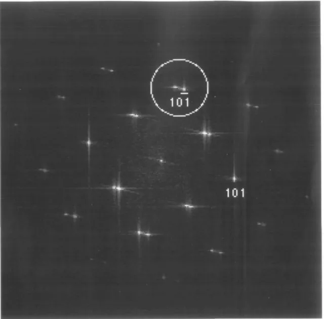
Fig. 2 Power spectrum of Rg. 1. The mask used for the calculation of the geometrical ghase is represented by the drde. The centre of the cirde corresponds to the reference redprocal lattice vector Jo and lies in the middle of the (101) peaks.
in each of the domains (which depend on the choice of the reference reciprocal lattice vectorg0) and cis a constant
phase term, E, and consequently the domain wall thickness
L can be determined by fitting equation 6 to the
geo-metrical phase measured experimentally.
Weak beam transmission electron microscopy When inclined domain walls are imaged using weak beam transmission electron microscopy [10], we observe well resolved thickness fringes across the boundary. By fitting simulated fringe profiles to experimental ones, we can extract the thickness of the domain walls in a quantitative way. A similar method also using the weak beam tech-nique has recently been used for the determination of the thickness of antiphase boundaries [11]. The simulation of the weak beam images is performed using the
Howie-Whelan approach of the dynamical theory of electron diffraction. For simplicity we introduce the column approximation [12,13], which is justified by the high electron energy (200-300 keV). The observed thickness fringes across the domain boundary are due to a local variation of the extinction errors ??, of the diffracted electron beams in the crystal. Thus, the values of the excitation errors are dependent on the position (x,y,z) of the electrons in the crystal and can be rewritten as ??1<# =
?,, + ]};•(& Idz. R(x,y,z) is the displacement field that describes the deviation of the unit cell positions due to the presence of the domain wall (deformable ion approximation). The displacement of the diffracting lattice planes is illustrated in Fig. 6a. One of the two adjacent domains is aligned with respect to the beam and satisfies the specified diffraction conditions, whereas in the other
I
Fig. 3 101 geometrical phase map. The phase can only take values between -JI (black) and JI (white) which induces phase jumps visible in the phase map by an abrupt variation in the grey levels.
P(x)
Fig. 4 Variation of the polarization across the domain boundary according to van der Waals. The asymptotic behaviour is indicated.
domain the crystal planes are displaced and therefore do not satisfy the diffraction conditions anymore. Therefore, the displacement field R varies from 0 on one side of the domain boundary to a linear displacement on the other side. The transition between those two regions has some spatial extension which is proportional to the thickness of the domain wall. By making the same considerations concerning the variation of the polarization across the domain wall as in the previous paragraph, we can immedi-ately express the displacement field as (Fig. 6b):
R (x) = R (x) =
for x < x0
(7)
+ (x - xQ)) for x
where d is a displacement vector depending on the crystal geometry. The shape of R is obviously very similar to the geometrical phase determined for the HREM method.
n in the unit cell. Mn = 8n2 <u2>n is the Debye-Waller factor with <u2>n being the mean square vibrational amplitude of atom «./rt'r' is the atomic scattering amplitude
in the first-order Born approximation. The expression for
(r) is
Vj w is similar to the one for V| <r), except that /n
replaced with the absorptive form factor/nw. The detailed
formalism for determining /n(r) and /n(/) can be found in
the work by Weickenmeier and Kohl [14].
Using the theory described above, we are able to compute the thickness fringe profiles that are observed on the weak beam images. The simulated profiles are then fitted to the experimental ones by varying simultan-eously the following simulation parameters: sample thickness, excitation error, absorption coefficient and the parameter {; describing the domain wall thickness. The fitting procedure is terminated when the mean square difference between the two profiles is minimized.
Results
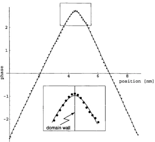
Both methods have been applied to 90° domain walls in PbTiO3. This material undergoes a first order phase transition at Tc = 492°C from a cubic paraelectric (7" > Tc) structure to a tetragonal ferroelectric one (T < Tc). The 90° domain walls are twins lying on {101} planes. Figure 1 shows a HREM micrograph of a 90° ferroelectric domain wall taken on a [010] zone axis (common to the two adjacent domains) using a Philips CM300 UT FEG micro-scope (accelerating voltage Vo = 300 kV, point to point resolution p = 0.17 nm). The corresponding power spec-trum is displayed on Fig. 2, the splitting of the peaks due to the twinning is clearly visible. The circle indicates the mask used to calculate the geometrical phase. Here, the (101) planes are chosen because they present the largest distortion. The reference reciprocal lattice vector is chosen precisely in the middle of the two (101) peaks, so that the geometrical phase is symmetric. The geometrical phase map is shown in Fig. 3. The abrupt changes from black to white in this image come from the -TI to K phase jumps. A line scan is made perpendicularly to the interface (see Fig. 5) and the domain wall thickness is extracted by fitting equation 6 to the obtained profile. The value for L is found to be 1.5 ± 0.3 nm.
Foeth et al. Quantitative measurement of ferroelectric domain walls 721
position [run]
Fig. 5 Variation of the geometrical phase perpendicular to the interface together with a fitted curve using equation 6. The centre of the domain wall is also determined by the fit (inset).
Foil normal Beam direction (a) Fault plane normal -Diffracting^ planes Effective thickness Displacement field R Domain wall fy>0 (T>OK) ^=0 (T=0K)
Fig. 6 (a) Displacement of diffracting lattice planes across the domain wall. The upper domain (light gray) is aligned with respect to the incident electron beam, whereas in the lower domain (dark gray) the crystal is not diffracting, (b) Continuous bending of the lattice planes across the domain wall due to finite temperature. The asymptotic behaviour of the plane bending results from an analogy with the variation of the polarization across the domain wall (Fig. 4).
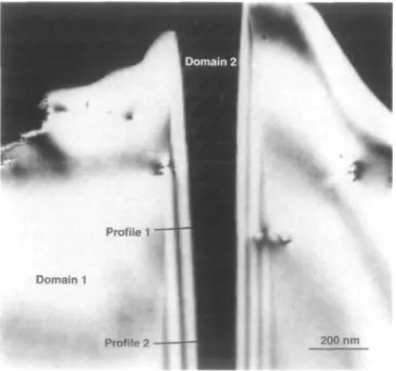
Figure 7 shows a weak beam image of a domain wall in PbTiO3 taken in g-2g diffracting conditions. In this case
9 = [TlO], the boundary plane is (Toi) and 2 =0.22[101].
Domain 1 is aligned in the specified diffracting conditions, whereas domain 2 appears dark since it is not diffracting. Well defined thickness fringes can be observed across the
ilar values are reported in the literature using HREM [4] or electron holography [15]. The minor discrepancy
Domain 1
Profile 2
Fig. 7 Weak beam transmission electron micrograph of a ferroelearic domain boundary taken in g—2g diffracting conditions. Well resolved thickness fringes are observed across the domain wall.
the domain wall which is needed for the weak beam image simulations. The weak beam method is on the other hand less concerned with sample quality and drift problems, can be performed on any classical TEM and should be easier to use at high temperature.
Conclusion
We successfully measured the thickness of ferroelearic domain walls in lead titanate using HREM on the one hand and WBTEM on the other hand. The results obtained are 1.5 ± 0.3 nm and 2.1 ± 0.7 nm respeaively, which is consistent considering the measurement accuracy. The two techniques are complementary in the sense that HREM is applied to very thin specimens (<10 nm), whereas WBTEM becomes accurate for samples thicker than 30 nm. Moreover, the atomistic struaure of the domain walls determined by HREM yields an accurate model which is used for the simulation of the WBTEM images. These techniques are currently being used to monitor the broadening of the ferroelearic domain walls as a funaion of temperature.
Acknowledgements
The authors would like to thank Prof. M. Robert and Z. L. Wang as well as Dr C. Beeli for valuable discussions.
0-25
20 40 60 80 100 120 140 100 120
x nm
Foeth et al Quantitative measurement of ferroelectric domain walls 723
This work is partially granted by the Swiss National Science Foundation Grant No. 20-42235.94.
References
1 Ishibashi Y (1989) Phenomenological theory of domain walls.
Ferroelectrics 98: 193-205.
2 Cao W and Cross L E (1991) Theory of tetragonal twin structures in ferroelectric perovskites with a first-order phase transition. Phys. Rev. 5 4 4 : 5 - 1 2 .
3 Robert M, Reaney I and Stadelmann P (1996) Critical interface in two dimensions. Physka A, 229: 47-52.
4 Stemmer S, Streiffer SK, Ernst F and Riihle M (1995) Atomistic structure of 90° domain walls in ferroelectric PbTiOj thin films. Phil.
Mag. A 71: 713-724.
5 Ross F M, Kilaas R, Snoeck E, Hytch M J, Thorel A and Normand L (1997) Quantitative analysis of displacement at 90° domain boundaries in BaTiO3 and PbTiC^. Symposium Mater. Res. Soc. IX,
245-252.
6 Hytch M J, Snoeck E and Kilaas R (1998) Quantitative measurement of displacement and strain fields from HREM micrographs.
Ultramicroscopy 74 (3): 131-146.
7 van der Waals J D (1894) Thermodynamische Theorie der Kapillaritat unter Voraussetzung stetiger Dichteanderung. Z. Phys. Chem. XIII: 657-725.
8 Widom B (1965) Equation of state in the neighborhood of the critical point. J. Chem. Phys. 43: 3898.
9 Foeth M, Stadelmann P and Buffat P-A (1999) Quantitative determination of the thickness of ferroelectric domain walls using weak beam transmission electron microscopy. Ultramicroscopy 75 (4): 203-213.
10 Cockayne D J H, Ray I L F and Whelan M J (1969) Investigation of dislocation strain fields using weak beam. Phil. Mag. 20: 1265-1270. 11 Le Floc'h D, Loiseau A, Ricolleau Ch, Barreteau C, Caudron R and
Ducastelle F (1999) Critical behavior of antiphase boundaries in Fe3Al close to the DO3-B2 phase transition. Phys. Rev. Lett. 81:
2272-2275.
12 Whelan M J and Hirsch P B (1957) Electron diffraction from crystals containing stacking faults. Phil. Mag. 2: 1121-1142.
13 Howie A and Basinski Z S (1967) Approximations of the dynamical theory of diffraction contrast. Phil. Mag. 17: 1039-1063.
14 Weickenmeier A and Kohl H (1991) Computation of absorptive form factors for high-energy electron diffraction. Atta Cryst. A-47: 590-597. 15 Zhang X, Hashimoto T and Joy DC (1992) Elearon holography study
![Fig. 1 HREM micrograph of a 90° ferroelectric domain wall in PbTiO, taken on a |0I0] zone axis.](https://thumb-eu.123doks.com/thumbv2/123doknet/14911644.658900/2.921.88.452.87.449/fig-hrem-micrograph-ferroelectric-domain-wall-pbtio-taken.webp)