HAL Id: jpa-00249636
https://hal.archives-ouvertes.fr/jpa-00249636
Submitted on 1 Jan 1997
HAL is a multi-disciplinary open access
archive for the deposit and dissemination of
sci-entific research documents, whether they are
pub-lished or not. The documents may come from
teaching and research institutions in France or
abroad, or from public or private research centers.
L’archive ouverte pluridisciplinaire HAL, est
destinée au dépôt et à la diffusion de documents
scientifiques de niveau recherche, publiés ou non,
émanant des établissements d’enseignement et de
recherche français ou étrangers, des laboratoires
publics ou privés.
Ferroelectric Domain Walls in BaTiO3: Fingerprints in
XRPD Diagrams and Quantitative HRTEM Image
Analysis
N. Floquet, C. Valot, M. Mesnier, J. Niepce, Laurent Normand, Alain Thorel,
R. Kilaas
To cite this version:
N. Floquet, C. Valot, M. Mesnier, J. Niepce, Laurent Normand, et al.. Ferroelectric Domain Walls
in BaTiO3: Fingerprints in XRPD Diagrams and Quantitative HRTEM Image Analysis. Journal de
Physique III, EDP Sciences, 1997, 7 (6), pp.1105-1128. �10.1051/jp3:1997180�. �jpa-00249636�
Ferroelectric
Domain
Walls
in
BaTi03:
Fingerprints
in
XRPD
Diagrams
and
Quantitative
HRTEM
Image Analysis
N.
Floquet
(~,~,*),
C-M-Valot
(~),
M-T- Mesnier(~),
J-C-Niepce (~),
L.
Norrnand
(~),
A.Thorel
(~)
and R. Kilaas(~)
(~) Centre de Recherche sur les mAcanismes de croissance cristalhne
(**), Campus
deLuminy,
Case 913, 13288 Marseille Cedex 9, France
(~) Laboratoire de Recherche sur la R#activitA des Solides
(***),
UniversitA deBourgogne,
BP 138, 21004Dijon Cedex,
France(~) Centre des Mat4riaux de
I'#cole
des Mines deParis,
BP 87, 91003#vry
Cedex,
France (~) National Center for ElectronMicroscopy,
Materials Sciences Division, LawrenceBerkeley
National
Laboratory,
University
ofCalifornia,
Berkeley,
CA94720,
USA(Received
1July
1996,accepted
12 Noi,ember1996)
PACS.77.84
Dy
Niobates, titanates,tantalates,
PZT,
ceramics, etc.PACS.61.14.-x Electron diffraction and
scattering
PACS 61.16
Bg
Transmission,
reflection and scanning electron microscopy(including EBIC)
Abstract. The structure of ferroelectric domain walls in BaTi03 has been
investigated
through
twocomplementary
approaches,
aglobal
oneby
the fineanalysh
ofX-ray
diffractionpatterns, the other
essentially
local ma a quantitativeimage analysis
methoddeveloped
andapplied
toHigh
Resolution Transmission ElectronMicroscopy
images.
These twooriginal
ap-proaches converge towards a clear
description
of 90° walls which are shown to be a 4-6 nmwide region where the
crystallographic
discontinuity
is accommodatedby
irregular
atomicdis-placements.
The resultsgiven
here demonstrate that the usual structural theoreticaldescription
of walls
commonly
accepted for energy calculations are far toosimplistic
The twounderlying
methodologies
which have beendeveloped
to carry out theseapproaches
canpossibly
beap-plied to other
ferroelectrics,
but without any doubt to other systems where twins or coherentinterfaces are
expected
R4sum4. Une 4tude de la structure des murs de domaines
ferrodlectriques
dans BaTi03est r4alis4e h travers deux
approches
comp14mentaires
: uneapproche
globale
par une m4thodefine
d'analyse
desdiagrammes
depoudre
de diffraction des rayons X, et une autre trAs localepar une m4thode quantitative
d~analyse
desimages
obtenues par microscopie41ectronique
dehaute r4solution. Ces deux
approches
originales
convergent vers une description Claire des mursde domaines h 90°
: c'est une
r4gion large
de 4-6 nm oh la discontinuit4cristallographique
estaccommod4e par des
ddplacements
atomiques
irr4guliers.
Ces r4sultats montrent que la descrip-tion structuralethdorique
commundment utilisde pour des calculsd'dnergies
est de loin tropsimpliste.
Lesmdthodologies
ddveloppdes,
propres h chacune desanalyses
structuralesutilisdes,
peuvent Atre
appliqu4es
h l'4tude de tout autre mat4riauferrodlectrique,
mais aussi h tout autremat4riau cristallis4 off des
maclages
ou interfaces coh4rentes sont attendues.(*)
Author forcorrespondence
(e-mail:
floquet©crmc2.univ-mrs,h)
I'*)
UPR 7251 CNRS(***) UMR 5613 CNRS
1. Introduction
The ferroelectric domain microstructure in
BaTi03
single
crystals,
powders
and ceramics hasbeen observed
by
manytechniques (Optical
Microscopy
11,2],
Scanning
ElectronMicroscopy
[3],
Transmission Electron
Microscopy
[2,4-6]
andrecently
Atomic ForceMicroscopy
[7,
8]).
Fromthese
observations,
descriptions
of the domain microstructure has beenproposed
[9]showing
that the domains are limited
by
twotypes
if
walls: the 90° and 180° ferroelectric domain wallsthat
correspond
respectively
to(101)
and(100)
crystallographic
planes.
However,
concerning
the fine wall structure
only
few observations and theoreticaldescriptions
have beenpublished.
Thus,
a limited number of researchers have carried out Transmission ElectronMicroscopy
to
study
the structure and thickness of domain walls in ferroelectric or related materials11,
5,10-12].
Twin walls inYBa2Cu307
have been observedby
High
Resolution ElectronMicroscopy
(HRTEM)
by
Zhu et al.[13,14],
domain walls inBaTi03
andLiTa03
have beenstudied ma the same
technique by
Bursill et al.[15],
and detailed observations onBaTi03
havebeen
reported
by
Tsai et al.[16]
and Normand et al.ii?]:
nevertheless,
none of these studieshas
given
direct evidence of aprecise
andquantitative
measurement ofdisplacements
anddis-tortions associated with the domain walls.
Using,
in a TEM methods derived fromholography,
Zhang
et al. haveproposed
a fineanalysis
of the domain walls structure inBaTi03
based on variations of theintensity
of thepolarization
vector[18]
that agrees with the "kink" modeldeveloped by
Zhirnov.Combining
HRTEM andImage Analysis,
Stemmer et al.jig]
have useda
quasi-lD
approach
to characterize the variations of the unit cellparameter
perpendicular
tothe
wall,
anapproach
that fits theconcept
of the soliton model[20];
but in either case localdeformations or
steps
cannot be detected.In this paper, we attempt to
give
a finedescription
of the domain wall structureby
twocomplementary
approaches.
The first one is athorough
analysis
ofX-ray
diffractionpatterns,
given
that the XRDdiagram
includesfingerprints
of the ferroelectric domain microstructureand
particularly
the domain walls. The second one is aquantitative
analysis
of the HRTEMimages seeing
that the HRTEM allows to visualize the atomicdisplacements
at theboundary
of two ferroelectric domains.
2. Ferroelectric Microstructure and
Crystalline
Structure ofa FerroelectricMaterial
2.1.
BaTi031
A FERROELECTR~C MATER~AL. At roomtemperature,
the structure ofBaTi03
istetragonal
with acla
ratio very close to I(cla
=1.01).
The material is ferroelectricbecause in the
tetragonal
cell,
thepositive
andnegative
charges
barycenters
do notcoincide,
thereby
inducing
aspontaneous
polarization
parallel
to the c-axis. Toadapt
itself to thecell
polarization,
the material is divided into ferroelectric domains characterizedby
a uniformpolarization
vector. The ferroelectric domainarrangement,
antiparallel
(180°
domains)
andperpendicular (90° domains),
minimizes the overall deformation and the electrostatic energy.A schematic ferroelectric microstructure is drawn in
Figure
la.2.2. RELAT~O~I BETWEE~I CRYSTALL~~IE STRUCTURE A~ID FERROELECTR~C
M~CROSTRUC-TuRE. The
crystalline
structure and the ferroelectric microstructure are inclosely
related.. The
polarization
vector isparallel
to the[001]
axis of the cell.. The ferroelectric domain walls are
usually
as sketched inFigure
1:(101)
or(011)
twinplanes
for 90°domains;
note that theangle
between the[001j
directionsfor two
adjacent
domains isexactly
2arctg(a
/c)
= 89 43°(Fig.
2)
180° ferroelccUic 90° fmoelcctric dorn@ns ~
f
~ ~ 180° (100) ou (010) (101) ou polarizationvector
Fig.
1. Relation betweencrystal
structure and ferroelectric microstructure schematic ferroelectric microstructure of the area selected in themagnifying glass
ofFigure
3.Domaln I Domain 2
~a
a~
c c
Pi
Fig.
2.(101)
twinplanes
for 90° domains: the trueangle
between thepolarization
directions fortwo
adjacent
90° domains isexactly
[2arctan(a/c)]°.
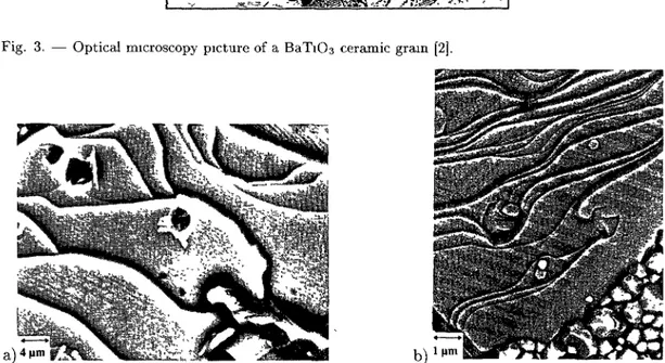
Figure
3 shows anoptical
microscopy
picture
of aBaTi03
ceramicgrain
(reported
by
Arlt
[2]):
the ferroelectric microstructure appears aslarge
strips
going
through
thegrain.
Each
strip
is divided into two sets of narrowstrips
which are 90° domains. The 90° domainwalls are, in one
large
strip,
either(011)
or(01i)
planes
and in theadjacent
large
strips,
either(101)
or(10T).
Twoadjacent large
strips
areseparated by
either(110)
or(T10) planes.
Notethat in this
optical
picture,
the 180° domains walls are not revealed.They
would appear inthe
magnifying glass
ofFigure
3 asrepresented
inFigure
1.Back Scattered Electron observations
by
Scanning
ElectronMicroscopy
(SEM)
of freesur-faces of a sintered
polycrystalline
sample gives
complementary
details on thegeneral
domainconfigurationj
in such SEMimages (Figs.
4a and4b)
where the contrast iscrystallographic
and due to the
slight
misorientation between twoadjacent
domains,
one can observe atypical
configuration
on(100)
growth
terraces. Oursystematic
SEMstudy
of thegeneral
arrangement
ioi ioi
iio
Fig.
3.Optical
microscopy picture of a BaTi03 ceramic grain [2].W
M
~~a)
4 Pm
-b)
Fig
4. SEM back scatteredimages
showing
atypical
domainconfiguration
on(100)
growth
terraces; the
"herring-bone"
structure isclearly
visible mla).
Because of the
relationships
between thecrystalline
structure and the ferroelectricmi-crostructure,
aBaTi03
grain
looks like amultiple
twinnedcrystal.
Thepowder
XRDdiagram
of
BaTi03
should contain thefingerprints
of this ferroelectric microstructure.Thus,
a full andaccurate XRD
study
was carried out in order tofully
describe the ferroelectric microstructure.3.
Fingerprints
of the Ferroelectric Microstructure Revealed in theBaTi03
XRDDiagram
In order to reveal these
fingerprints,
asimple
solution consisted invarying
the ferroelectricdomain microstructure in a known manner ~N"hile
recording
the XRDdiagrams.
After a briefpresentation
of theBaTi03
XRDdiagram,
it will be shown how thisdiagram
evolves,
on theone
hand,
by
applying
anincreasing
electric field to the ceraJnic materialand,
on the otherIntensit ~~ ~-o c4= ~~~
§ §
~
~ ~~ ~~~ ~~ 25 30 35 40 45 50 55 60 28 j °) Intensit 48
~
~T1i8
rise $z = ~j~8~
S~Sti$ 3 8c4 c4 oc4c4~n -~n~n -~n c4 c4~n~n c4~nrn o+ 65 70 75 80 85 90 95 IOO 28 °) Intensit +c~ 2000 _ ~~_~ ~_ ~gg
+~jp
Q@ gQfl)fl@)z@Q@
Q~@iWW
iiW" °'~' l05 1lO 115 120 125 130 135 140 28 °Fig.
5 Indexed BaTi03 XRDdiagram.
3.1.
BaTi03
XRPD D~AGRAM. Thepowder
XRDdiagram
oftetragonal
ferroelectricBaTi03
isrepresented
inFigure
5. As for atetragonal
structure material withcla
ratio closeto
1,
thediagram
iscomposed
ofsingle
lines and of doublets andtriplets.
The
single
lines aresymmetrical
as for an "usual"crystalline
material.By
contrast,
thedoublets and
triplets
have veryparticular
profiles.
The doubletprofiles
could be described intwo different way-s:
the sum of two
dissymmetrical
lines,
with thedissymmetry
inside the doublet(Fig. 6a)
the sum of two
symmetrical
lines withspecific
diffracted intensities in the two lines andof a
particular
diffractedintensity
between the lines(Fig.
6b).
The
study
of the XRDdiagram
evolution as a function ofphysical
factors,
such as theelectric field and the
temperature,
allowed tohighlight
twofingerprints
of the ferroelectricdomain
microstructure,
the relative intensities of two lines of a
doublet,
the
symmetrical
profiles
of thesimple
lines. It also confirmed that theparticular
profiles
of doublets and
triplets
are domain microstructurefingerprints.
3.2. RELAT~VE I~ITE~IS~TY OF THE ASSOC~ATED L~~IES: POLAR~ZAT~O~I STATE OF THE
MATER~AL. In sit~ XRD
experiments
allowed to record the XRDdiagram
of a ceramicdisk of
BaTi03,
when an electric field isapplied
perpendicularly
to it. Anexperimental
de-vice was
specially
built for this purpose.Thus,
XRDdiagrams
of theBaTi03
ceramic wereregistered
as a function of theapplied
electric field.Why
apply
an electric field to a ceramic? In order to force the material toadapt
itself tothis external strain
by
modifying
its domain microstructure and thus to record thepossible
"Symmetrical
linedescription"
m~pple-Way d©racwd Mtend~
Wtween We tm lines
~)
M-S 45 45.5 46"Dissyrnmetrical
linedescription"
b)
M-S 45 45.5 46Fig.
6. Two ways for the doublet linedescription
in the BaTi03 XRDdiagram: a)
dissymmetric
description,
b)
symmetric description.The electric field effect is shown in the XRD
diagram
by
an evolution of the relative intensitiesof the diffraction lines. For
example
in the 002/200
doublet,
when the electric field isincreased,
the
intensity
of the 002 line increases at the expense of the 200 line(Fig. 7).
This can beexplained
by
the motion of the ferroelectric domains wallsinducing
thegrowth
of the domainswith a
polarization
vector closest to the electric field. Thepolarization
directionbeing
parallel
to the
c-axis,
the(001)
plane
familiesproportionally
increase at the expense of the(100)
plane
families
(Fig. 8).
The relative intensities of the doublet lines express thepolarization
state ofthe material
[21].
The curve R
=
f(E) (Fig. 8),
obtained from the diffractedintensity
measurements,
iscom-pared
to the schematic firstpolarization
curveP/Ps
=f(E).
Electric
polarization
measurements and XRD do notanalyze
thepolarization
state on the sameway:
the electric measurements consider the whole
sample volume,
with all thegrains
(what-ever their
orientation),
with all the domains(180°
and90°)
XRD considers
only
the surfacela
fewmm)
andonly
somegrains
(that
are in diffractionooi loo 1071 V/mm ', 1o7i I
j''--, 7l4Vlmm ~~ tKn,im 2<n ' field ' 536 Vlmm , unpalkd Mate Mvlmm 44 5 44 7 44 9 45 45,3 45 ,~ 45 7 26(°)Fig.
7. Evolution of the002/200
doublet as the electric field increases.' ~ l~~~
(l~~~
)~~~~
~ ~002 + ~200 ~~~002 ~uc 0.8 0.8 0.6 o 0.6 DA DA o-z o-z 0 ZOO 600 800 lZ00_~
f~+
~-- _~~
~ ~~
-~ mpoled°~ ~"
(°)
/
~'
ii1 222 333 ~so~ Ferroeleciric ~~domilin
150°C/450°C Paroelec~ic classical microdistorsions ° °~ ° ~ sin(fl)
/ X
Fig.
9Experimental
proof
of the domain wall contribution as lattice microdistorsions to the linebroadening
The
comparative
interpretations
of the R andP/Ps
curves allow to characterize the domainwall motion under the influence of the electric field. The 180° domain wall motion occurs for
a very low value of the electric field for which R =
0,
whereas the 90° domain walls move fora
higher
value of the electric fieldcorresponding
to R > 0.This
study
shows thatX-ray
diffraction couldbe,
when associated with electricmeasure-ments,
aquantitative
tool todistinguish
theenergies
required
for 90° and 180° domain wallmotion under an external strain effect.
3.3. S~~GLE LmE PROF~LES: DOMA~~ WALLS As M~cRoD~sToRTm~s.
Contrary
to thedouble
lines,
theprofile
of thesingle
line is well defined. Thestudy
of the hhh linebroadening
with
temperature,
through
a Williamson and Hall[22j
plot
shouldbring
qualitative
data onthe
crystallite
size(coherent
diffractionsize)
and lattice microdistortion of the material. TheW-H
diagram
consists in astraight
line with theorigin
ordinateleading
to the meanapparent
crystallite
size and theslope
to the meanapparent
defect ratio in the directionperpendicular
to the hkl
planes
being
considered.The XRD
diagrams
were collected in LUREusing
the D23 diffractometer[23j.
The resultsare
presented
in a W-Hplot
of the hhh lines as a function of thetemperature
(Fig. 9).
As the
temperature
increases up to thephase
transitiontemperature
Tc,
theslope
decreases.For
temperatures
aboveTc
(Tc
< T < 450°C),
there is no more evolution of theslope.
At low
temperatures
IT
<Tc),
the decrease of thebroadening
cannot to beexplained by
aclassical lattice distortion relaxation
(in
such a case, this relaxation will not stop atTc).
Butthen,
it ispossible
toexplain
this decreaseby
the relaxation ofparticular
microdistortions:the ferroelectric domain wall. As the
tetragonality
decreases withtemperature,
the domainwalls are less and less a defect
given
that the lattice misfit between twoadjacent
domains isdecreasing (Fig. 10).
The contribution of the domain wall to theslope (Sdw) decreases,
tofinally
disappear
atTc
when theBaTi03
lattice becomes cubic.For
Tc
< T < 450 °C,
there are no ferroelectric domains left and the value of theslope
represents
only
classical microdistortions(Sid).
Such aninterpretation
is consistent with~ ~~
~all(101)
~ ~ ~ ~ ~~~~~j
,~~
,N~
~j
cfl
~
~
~
~
~
~
~
cla=1.011
magonal
Cubic cla=IT >
Fig.
10.Diagrammatic
representation of a domain wall between two 90°adjacent
ferroelectricdomains as a function of temperature: increasing the temperature,
decreasing
theparticular
lattice distortions that are the ferroelectric domain walls.ferroelectricity
isreversible,
theslope
and theapparent
defect ratio due to the domain wallsreturn to their initial values.
Note that in this
study,
theorigin
ordinate remainsapproximately
equal
to zero and has noreal
significance.
This is due to thelarge
grain
size;
thus theapproximation
of the infinite sizecrystal
is valid allalong
thisstudy.
The
study
of the hhh linebroadening
by
this method as a function of the temperature, showsthat the ferroelectric domain walls contribute to the hhh line width. This result proves that
the ferroelectric domain walls act as
particular
lattice microdistortions.3.4. PARTICULAR PROF~LES OF DOUBLETS A~ID TRIPLETSI STRESS STATE OF THE
FERROELECTR~C DOMA~~I M~CROSTRUCTURE
3.4.1. Influence of an Electric Field on a
BaTi03
Ceramic. The most visible modificationof the XRD
diagram
as a function of electric field is the evolution of the intensities of the lines(3.2.).
However,
athorough
study
shows that theparticular
profile
of doublet ortriplet,
due toa
supplement.ary
diffractedintensity
between thelines,
evolves with the electric field(Fig.
7).
This
particular
intensity,
denotedIoo2-200,
has been evaluatedby
assuming
asymmetric
profile
of each line withrespective
intensitiesIoo2
andI200
(Fig.
6b).
The
integrated
intensity
ratio of the two lines(Ioo2
/I200)
increases with the electric field(E)
whereas the relative
intensity
between the 002-200 double lines(Ioo2-200/(Ioo2
+I200))
goesthrough
a maximum(Fig. 11).
The curveIoo2-200
"f(E)
is similar to the derivative of thecurve
Ioo2/I200
#f(E).
Its maximum(Ioo2-200/(Ioo2
+I200)
"0.85)
matches the maximumof transformation rate of the 90° ferroelectric domains
(Ioo2/I200
"2).
As the evolution ofthe microstructure is at its maximum under the electric field
effect,
the diffractedintensity
between the double lines is at its maximum too.
Thus,
thatparticular
diffractedintensity
wellcharacterizes the ferroelectric domain microstructure and is related to the stresses induced
by
the domain wall motion.
3.4.2. Influence of the
Temperature
on a Powder.Heating
aBaTi03
Powder
above itstetragonal-cubic
transitiontemperature
(Tc
* 120 °C),
is an other way tomodify
andfinally
to remove the ferroelectric domain microstructure.The XRD
diagrams
were recorded at differenttemperatures,
from roomtemperature
up to350 °C
(Figs.
12,
13).
As thetemperature
increases up toTc,
the 002 and 200 line
positions
get
closer to the cubic 002 lineposition;
the ratio
Ioo2/I200
does notchange;
'ooz-zoo ' (I ooz+i
zoo)
~~z/tzoo o.9 s 4 0.7 3 0.6 z DA -200 E(V/mm)Fig.
11.Comparison
between the 002 and 200 line intensities and theparticular
intensity
betweenthe doublet lines as a function of electric field
1 (200)c 140°C (002)q ~~~~~~ 94°C Temp 75°C 002-200 200 ~ 5)°c 44. 6 44. 8 45 45.2 45.4 45.6 45.8 29 °
Fig.
12. Evolution of the 002/200
doublet lines as a function of temperature.As the
tetragonality
decreases withtemperature,
the microstructureprogressively
vanishes.Thus,
this diffractedintensity
between the two lines of a doublet shouldagain
be related withthe ferroelectric domain microstructure.
a , c
I
~nnz-2oo
4.03 5° c 4,02 4O 30 4.Ol ~ 20 4 io 3.99 o 3.98 20 40 60 80 loo 120 tC tUle ~°t~~Fig.
13.Comparison
between the lattice parameter evolution and theparticular
intensity
betweenthe doublet line evolution as a function of temperature.
(Figs.
7,
12),
probably
due to the mechanical and electrostatic interactions of eachgrain
of the ceramic with itsneighbours
[24].
This difference between the "stressed" microstructureof a
grain
in a ceramic and the "free" microstructure of thegrain
in apowder
explains
thedifference in the diffracted
intensity
between the two double lines.3.5. PART~CULAR PROF~LES OF DOUBLETS A~ID TR~PLETSI A COHERE~IT CO~ITR~BUT~O~I ~~l
THE WHOLE D~AGRAM. The
particular
diffractedintensity
between the(002
/200)
doubletis
related
to the ferroelectric domain walls. As a wall cuts everycrystalline
plane
except
itself,
the effect of the domain walls should appear in all hkl lines
and,
moreover, their contributionwould have to be coherent in the whole
diffractogram.
The XRD
diagram
was recordedusing
a 9-29goniometer
(Siemens
D500)
[25].
A coarsegrained
BaTi03
Powder,
with a narrowgrain
size distribution(1-2 ~m),
has been used inorder to
get
wellseparated
lines of doublets andtriplets.
Two
complementary
ways ofinvestigation
wereperformed
in order to describe theparticular
diffracted
intensity
between the lines.3.5.1.
Dissymmetrical
LineDescription.
In this first way ofinvestigation,
a doublet or atriplet
is considered as a sum of two or threedissymmetrical
lines. Each line of the wholediagram
was fitted to adissymmetrical
Pearson VII function without anyphysical
criterion.The Siemens Profile software is used. The line
dissymmetry
isrepresented
by
the ratio of theintegrated
width of the left half over theintegrated
width of theright
half of the line. Thisratio,
notedf,
isgreater
than I if the line is leftdissymmetrical,
smaller than I if the line isright
dissymmetrical,
andequals
to I if the line issymmetrical.
Aberrantfits,
occurring
forvery mixed
lines,
are excluded.To
give
asynthetic
view of theresults,
astereographic
projection
is used. The(001)
stereo-graphic
projection
(Fig. 14a)
shows the[011]
and[101]
meridians and theirequivalents
CZZ zone I f <1 ~. ~. '" CZ zone 2 f >
'~jj
(l10) .; ~,-C~2zcne3f >1[
' loll) ~'~~'j
, '' /~_ " i ;'[ Zone ~ (001)~i'
©(412) ',joii)
jiio)
"i
[°
l~~°)
°°°,hhh mhhi/oihh A boil
Aioh/A
rho/Kr hhl . hkl/ olkh/ o link
a)
b)
Fig
14. Dissymmetry factor ofthe diffraction lines represented in the(001)
stereographic
projection
of the BaTi03 structure:
a)
wholeprojection;
b)
focusedprojection
of the nonequivalent
hkl linesthrough
thecubic-tetragonal
transformation: one line of the cubic structuresplits
in threelines of the
tetragonal
structure.Figure
14b focuses on all nonequivalent
hkl lines. The doublet lines are on the[110],
[0Tl],
[T01]
meridians. The two lines of ahhl/lhh
doublet are on[lT0]
and[011]
meridiansrespectively.
The two lines of ahlh/hhl
doublet are on[T01]
and[lT0]
meridiansrespectively.
The lines on the
[lT0]
meridians have half theintensity
of the lines on the two other meridiansdue to the difference of
multiplicity.
The
h01/10h/lh0
triplet
lines are on the[010]
and[001]
meridians. The first one is on the[010]
between(001)
and(101).
The second one is on the[010j
between(100)
and(101).
Thethird one is on the
[001]
between(100)
and(l10).
Each line of thehkl/lkh/lhk
triplet
is inone of the three areas. All the
triplet
lines are of sameintensity
becausethey
have the samenumber of
equivalents.
The
dissymmetries
f
of the lines arereported
inFigure
14. Theright
dissymmetrical
linesif
= 0.6 to
0.8)
are in the areaI,
thenearly
symmetric
linesif
r~I)
are in the area2 and
the left
dissymmetrical
linesif
= 1.2 to lA are in the area 3.
These
results prove that thedissymmetry
of all thediffractogram
lines is coherent with theBaTi03
tetragonal
structure.For each
doublet,
the ratio of the first linedissymmetry
ratio over the second linedissym-metry
ratioiii /f2)
isnearly
constant. This proves that thedissymmetry
is the same whateverthe doublet. Note
that,
in adoublet,
the first line isright
dissymmetrical
whereas the secondis left
dissymmetrical.
This result is inagreement
with thesupplementary
diffractedintensity
observed between the two lines of a doublet.
For the
triplets,
the first line isright
dissymmetrical,
the second,isnearly
symmetrical
andthe third is left
dissymmetrical.
This observation evidences that atriplet
must beanalyzed
as three doublets
by associating
the linespairwise:
the first line of thetriplet
isalways
right
lalensll, ~~P~~""~ P~°~* 200 Synlnlelncal profik 002 o ~ e (o~
~)
44.5 45 45.5 46 lateasll, Expenmenw prorde 311 Symme~ncaJ pmfile I 13 o ~~~~~~~~~ 2 6 (°)bj
78 78,5 79 79.5 80 80.5Fig
15. Manifestation of a"plateau"
between the lines of a doublet.always
leftdissymmetrical
because its counterparts are the first and the secondlines;
the secondone is
always
nearly
symmetric
because it is leftdissymmetrical
with its leftcounterpart
(the
first
line)
andright
dissymmetrical
with itsright
counterpart(the
thirdline).
3.5.2.
Symmetrical
LineDescription
3.5.2.I. Manifestation of a "Plateau" Between the Lines of a Doublet. In the second way of
investigation,
theprofile
of a doublet is considered as a sum of twosymmetrical
lines andof a
supplementary
diffractedintensity
between the lines. The leftpart
of the left line andthe
right
part
of theright
line are well defined. Two calculatedsymmetrical
lines are builtby
"symmetrizing"
the two well defined halfprofiles.
The twosymmetrical
resulting
lines aresubtracted from the
experimental
profile
of the doublet. The difference looks like arectangular
function called a
"plateau",
with thesymmetrical
line maxima as ends. All the doublets canbe described with this model
(Fig, is).
The
plateau
intensity
ranges between 8 and12%
of the doubletintensity.
The4%
intensity
error comes from the lack of
precision
in the 29position
choice of the line maxima. A small error in the maxima choice induces aimportant
error in theplateau
intensity.
Whatever thedoublet,
theplateau
intensity
isnearly
constant withrespect
to the doubletintensity.
The°~*~' » a rw~wr _ _ ~ r,iw.i ~_ kw i i o,e o.4 o,a o 29.5 30 30,5 31 lo 29,8 30 30.5 al lo 29,5 30 30.5 31
a)
b)
c)
Fig.
16. Plateau model for the doubletsla)
and thetriplets
(b, c).
The doublet
intensity
could beexpressed
by:
Idoubiet
"(Ihhi
+[hh
+pd)
with[hh
"2Ihhi
ifh < and
Ihhi
"2[hh
if h > and pd " doubletplateau
intensity,
with pd " Pdmax xA29,
pdmaxbeing
theintensity
maximum of theplateau
and A29being
theangular
difference between thetwo lines.
Thus,
as observed inFigure
is,
theintensity
maximum of theplateau
depends
onthe
angular
difference between the two lines.3.5.2.2. "Plateau" Model
Applied
to theTriplets.
As shownpreviously,
atriplet
is made oftwo
by
two associatedlines,
thus theplateau
model can beapplied
in the same way. Thetriplet
intensity
could beexpressed by:
Itr,plot
"(Ihki
+[kh
+Ihik
+pt).
For the sake ofconciseness,
Ihki
"Ii, [kh
"12, Ihik
"13,
withIi
# 12 #13.
Pt is thesupplementary
integrated
intensity
between all the lines taken
pairwise:
Pt " P12 + P23 + P13 With p12 " P12max X
1i2912>
P23 " P23maxX1i2923>
P13 " P13max X1~2913.
Since a doublet is a
particular
triplet,
thesupplementary
intensity
between the lines is assumedto be the same in a doublet and a
triplet:
pt/Itr,plot
"Pd/Idoubiet
and p12 " P23 " P13 "pt/3.
Thus,
in atriplet,
the threeplateau
maxima will have differentvalues,
depending
on theangular
position
of the middle line(Fig. 16).
The
dissymmetry
approach
has shown that the doublet and thetriplet
could beanalyzed
inthe same way. No
(hkl)
plane family
seems to beparticular.
Thisanalysis
well proves thatthe character of the
profile
is coherent in the wholediagram.
Theplateau
model confirms thiscoherence and allows to
bring
a clear distinction between thediffractogram
particularities
ofsuch a
tetragonal
ferroelectric material from thediffractogram
of a classicaltetragonal
materialwithout microdistortion.
3.6. "PLATEAU" MODEL A~ID STRUCTURAL DESCR~PT~O~I OF THE 90° DOMA~~I WALLS.
By
these twoapproaches
theparticular profiles
could beinterpreted
by
aninterplanar
distancedistribution in the material. The
plateau
model shows that this distribution is constant andthe
interplanar
distance varies between theinterplanar
distances of the twocounterpart
planes.
The two
counterpart
planes
could be deduced from each otherby
a mirrorsymmetry
about(101)
or(011)
planes.
Also,
two 90° ferroelectric domainscorrespond
to each otherby
thesame mirror
symmetry
planes
that are the boundaries between two 90° domains.Thus,
thesymmetrical
lines come from the diffraction of the ferroelectric domains whereasthe
plateau
comes from a misfitboundary
area between them. Thisinterpretation
suggests
that the 90° ferroelectric domain walls are not twin
planes
but misfitboundary
area. TheFig.
17. Plateau model and evolution of thecrystalline
lattice inside a 90° domain wall.planes
whichinterplanar
distance varies from the hklinterplanar
distance in one of the 90°domain to the lkh or hlk
counterpart
distance in theadjacent
domain(Fig. 17).
4.
Quantitative
High
Resolution TEMImage
Analysis
A transmission electron
microscopy
study
has been carried out in order to cross-checkby
a morelocalized
investigation
theapproach
by X-ray
diffraction described above.First,
conventionalTEM and electron diffraction have been
performed
to obtain an overall characterization andlocalization of the domain wall structure as well as a
long
range measurement of the twinangle
in ourmaterial;
then anoriginal
methodology
based on thequantitative
analysis
ofdigitized
HRTEMimages
has beendeveloped
in order to obtain aprecise
evaluation of atomicdisplacements
in the immediatevicinity
of 90° walls[26].
4.I. EXPERIME~TAL Sintered
polycrystalline
BaTi03
was cut into 3 mmdisks,
mechan-ically polished,
dimpled
and ion milled to obtain asample
transparent
to the electron beamObservations have been carried out at 800 kV on the Jeol Atomic Resolution
Microscope
(ARM1000),
and at 200 kV on a Jeol 200CX and aTopcon
0028.Samples
observed at 800 kVwere carbon coated to prevent from
charging
under the electron beam. HRTEMoriginal
nega-tives were scanned
by
use of a 6000 element C CD Leafscan 45 scanner connected to a Macintoshmicrocomputer;
1024 x 1024 or 2048 x 2048pixels
digitized
images
were obtained andana-lyzed
through
theDigital Micrograph
software.Digitization
must be carried out ~§.ithout anyinterpolation
and must allow thedescription
of an atomic column with 8~ to10~
pixels.
Theexisting
methods such as"template
matching"
has beenproved
not to be accurateenough
todetect atomic
displacements
at domain walls in our Inaterial. The calculation of the atomicdisplacements
was then carried outby
means ofspecific
subroutines which have beendevel£ped
as "custom functions" derived from the
"peak
finding"
technique.
4.2. CO~VE~T~O~AL TEM IMAGES.
Figure
18a shows atypical
view of 90° domain wallsFig.
18a)
Lowmagnification
TEMimage
takenalong
a(100)
zone axisshowing
90° domain walls;b)
Selected Area Diffraction Pattern of the zone indicatedby
a white frame inFigure
16a,enlargement
of a part of the SADP to enhance the
splitting
of the(011)
spots,cl High
Resolution TransmissionElectron
Microscopy
imaging
of the same selected area where theangle
between the(001) planes
acrossthe wall is indicated.
For
(100)
typeorientations,
two different diffractionpatterns
are found.for the so-called a-a walls
(when
the a-axis isparallel
to the electron beam for bothgrain),
the habitplane
isparallel
to the beam and thesplitting
of the reflections(0kk)
and
(0k-k)
ismaximum,
then the truelong
range twinangle
can be measured and reaches0.5° as can be seen in
Figure
18b;
this value is consistent with what isexpected
from thetetragonal
parameters obtained fromX-ray
diffraction and fromgeneral
considerationsof
crystallographic
models fortwinning;
for the so-called a-c walls
(when
the beam isparallel
to the a-axis of one domain and tothe c-axis of the
other)
the habitplane
is oriented 45° from the electron beam directionand 13 associated with a
fringe
contrast;
estimation of the twinangle
from diffraction4 3. STA~DARD A~ALYS~S OF HRTEM IMAGES.
Figure
18c shows a detail of the 90°walls seen in
Figure
18aimaged
by
theHigh
Resolutionimaging technique;
one can observethat
going
from diffraction contrast tophase
contrast diminishes the intrinsic contrast of thewall,
which is in certain casesextremely
difficult to locate. The 0.4° twinangle
is neverthelessfound,
even if the measurement is less easy than in the diffractionpattern.
But a 4-5 nm wideslight
diffuse dark contrast(about
10 unitcells)
associated with the wall can beclearly
seen.This has been observed in all HRTEM
images
of domain walls that have been taken.Furthermore we
systematically
observed inBaTi03
astrong
degradation
of thespatial
reso-lution of the HRTEM
images
in the immediatevicinity
of the walls. Since the distance betweenthe Ba atoms and the Ti atoms is very close to 0.2 nm, well within the excellent
capability
of the
microscopes
we have beenusing
(which
resolution ranges from 0,16 for the ARM to0.19 nm for the
Topcon
0028)
we couldexpect
routinely
toseparate
the two metallic atomsof the structure. We
only
succeeded to record suchimages
far away from any ~§"alls as can beseen in
Figure
18c where thespatial
resolution is better than 0.2 nm,allowing
thus the Ba andTi lattices to be
clearly
seen whereas it is at bestequal
to 0A nm close to a wall.Numerical
diffractograms
obtained from a Fourieranalysis
on 256 x 256pixel
areas(about
24 x 24 unit
cells)
centered on 90° walls reveal diffraction spots that are much more diffusethan when taken away from the
vicinity
of a wall.Diffractograms
taken from wider areas showin addition the
splitting
due to thesuperimposition
of thepatterns
relative to the two domainsas in the electron diffraction.
From these
preliminary
HRTEMobservations,
it can be inferred that the diffuse contrastassociated with the 90° walls could
originate
from'either local distorsions of theBaTi03
latticeor the modification of the
phase
of theincoming
electron waveby
the localpolarization.
Sincethe
respective
influence of these two contributions cannot beclearly
distinguished
on theob-served
contrast,
andowing
to the fact that structural distortions have immediate consequenceson the local
polarization,
we assumed in this paper that the contrast associated with the wallsin HRTEM
images
wasessentially
due to localdisplacements
of metallic ions in theBaTi03
lattice.
4.4.
QUA~IT~TAT~VE
A~IALYS~S OF HRTEM IMAGES4.4.1.
Principles
andExperimental
Conditions. Wedeveloped
"custom functions" derivedfrom the
"peak finding"
method in order toquantify
the atomicdisplacements
of metallic ionsassociated with the
specific
contrast of 90° walls in HRTEMimages.
Thelong
termgoal
ofsuch an
approach,
wellbeyond
the frame of this paper, is the evaluation of the behavior of thepolarization
vector across the wall andconsequently
the direct calculation of the wall energy.The
"peak
finding"
method is based on the search of local maxima ofintensity
in adigitized
image;
this isparticularly
easy in a HRTEMimage
provided
that an atomic column is describedby
asufficiently large enough
number ofpixels.
Sinceonly
the cell distortion is lookedfor,
it isnot necessary to restrain the
imaging
conditions to the case where a column of atoms isonly
white,
oronly
dark: theimportant
point
is that theimages
display
asharp
periodicity,
blackor
white,
corresponding
to the cations lattices. The Scherzer defocusimaging
conditions willpossibly
be chosen for itcorresponds
to the beststability
of themicroscope
contrast transferfunction over a wide range of
spatial
frequencies,
leading
then to the same contrast for thedifferent
types
of cations columns in theBaTi03
lattice(see
Fig.
19 for two different zoneaxes).
Eventhough
it is not ofprime
importance
to know whether atoms are black orwhite,
itis nevertheless
absolutely
essential to check that theexperimental
conditions(defocus,
thinness)
remain stable within the whole area under
considerations,
i.e. there is nobending
ofthe foil
O
Ba
c
Ti
<l00>
~
<lll>
~
~~
Fig.
19. HRTEMimages
ofBaTi03,
corresponding
contrast simulations on the upper left corners;a) along (100);
b)
along
(111).
such artifacts remain
negligible
and we have tried tostudy
walls orientedperpendicular
to ahole in the
sample
in order toget
rid of any thicknessgradient
across the wall(see Fig. 18a).
Defocus and thickness for the HRTEM
images
are to becarefully
cross-checked in associationwith contrast simulations.
Once the
"peak finding"
technique
wasadapted
to therequirements
of the HRTEMimages
of the
BaTi03
lattice,
we carried out the different sequences of our "custom function" basedon the
systematic
comparison
between aperfect
lattice,
created from a nonperturbed
region
of the HRTEM
image,
and the real lattice taken from thegeneral
viewincluding
the 90° wall:taking
into accountpixelation
noise as well as randomdisplacements,
the software translatesand
superimposes
automatically
the idealperfect
lattice to the real distorted oneby
steps
of onereticular distance. For each
step
it makes the calculation of the translation vectorcorresponding
to the
position
of the centers ofweight
for bothsuperimposed
cells. Results aregiven
under theshape
of maps where thesedisplacement
vectors areplotted,
the direction and modulus of thevectors
being
representative
of the direction andintensity
of the atomicdisplacements.
Theaccuracy then obtained is better than 0.01 nm. The
validity
of thetechnique
has been verifiedwhen
applied
to alarge
100 x 100 nm area free of any wall: nosignificant
atomicdisplacement
was found.
4.4.2. Results. Two
examples
of such aquantitative
treatment arepresented
inFigure
20aand 20b where one can see HRTEM
images
of 90° domains observedalong
a(100)
direction;
the walls
(indicated
by
whitearrows)
arebarely
located in theexperimental
images,
but are,.,,lilli"",',i,,i,,,<,,,,.,,,,,.;...;.:... -,,'lilll'l""',,,i,,,,i,,,,,i,,,,,,,,..,,;.;,,,+ .,'iiii'll"',',,i,,,,,,,,,,,,,,;<,,,,.,,,,.,,,,, ~-~ ,,,,'iiiill"'ii,,,i,,,,,,,,,,,,,,,,,,,,,,,,,,.,,, $~ .,,"'ii","ii,lint,,<,,i,,,,;.,,,,.,..,,..,,, o ,,"',,;,,,"t",,,,,,nil,,i,,,,,,1,,<.,,,,,,;.,,,,, ,~ ,,"",,,-i,,,,,,,,,,,,,,,,,,i,ii,,,,+;,+,,,,,,,,,,++,, """""'-""""tt""t't""'t't"'+o+"+>o'+-+,o+,'t ~j t""""',.,""""'t"""ttttt,tttttt"'ttt'""t'ttt' "'t""",+ ,,,,,,',"",,',,,,,,,,,,i,,,,,,ii,,,,i,,,iii _f~ ,,,,,""',,,--,,,,',,,,,,,,,,,,,,,,,,,,,i,,,i,,,,,,1,,,,, ~ 'tl'tt"'tt,,, .,,,,,,',,,,,,,,,,,,,,,,,,,,,i,,,,,,,,,,,, ,,,'ttttttit',,i,,,,,,,,,,,,,,,,,,,,,,,,,,,,,,,,,,,,,,,,,, q~ ,,t,ttitttttttt',,.-,,,,,,,,,,,,,,,,,,,,,,,,,,,,,,,,,,,,,, ~ ,,,,t'itttttiiitt,,,,-,,,,,,,,,,,,,,,,,,,,,,,,,,,,,,,, ~_~
.;,,,,'tttjjtittitttt,,,-,,,,,,,,,,,,,,,,,,,,,,,,,,,,,,,,
_ .,,,,,,,,tt.,<,,,',"tt
((j(I
t ] tttti~~-,,,,,,,,,,,,,,,,,,,,,,,,,,,jjt<I'--M""""""""""""/~
,o,o.,',,'tfJfJJjj
t I' ~J ;.j,,,,,iii f~
ii,£
-,~~~$$~~~(~~~~~(l~~~
""' ,, ---.-o"##i#ill,'tj "---~~f,,"",',-.-oo,'-,-,"~~~~~
j,"'-""'J( ~_~,,,,,,,,,,,,,,,,,,---,,,~~~
lifflt I'nil",,J,J,,,,,,,,,,---,,,~'~~~~~~~
~(~jjj)
~
>lint,",'J"""""'---"""iii'"i~~
' 'I»iii',,'£""""---'---'-"'~-~""'i~
""",,>'i'i,',""','-,---""'~ittt.,'ttt"",,'tt"",,,',,,,---""'~
,-,'ttt~"t',tl""',,,,-,-,,', 't..,"""t'ttt'<coo-,,,o,,,,-t~'t -""""~'t',,,-;oo.o,--- 't'-,""""',,,,o,o...o,,o,---o.-""""',';.. ooooa)
~
~~~~~
~~~~ ~~~~~~~~~
Fig.
20. HRTEMimages
of 90° domain walls and thecorresponding
atomic displacement vectorplots,
a)
the mapcorresponds
to the framed area m which the wall isarrowed;
the defect on whichthe wall is pinned is also indicated
by
white arrows; the perfect lattice has beengenerated
from thenon distorted area m the upper
right
corner of the HRTEM image;b)
the wall ishardly
seen on theHRTEM
image,
it appearsclearly
on the map where(100)
aregiven
evidence.The first and
straightforward
consequencebrought
by
these2D-displacement
maps is adirect and local confirmation of the structural
interpretation
given by
theX-ray
diffraction fineanalysis
earlier in this paper: 90° domain walls inBaTi03
can nolonger
simply
be consideredas
twinning
habitplanes,
but must be described as an area of a certain thickness(r~
5nm)
across which the cell parameters vary more or lesscontinuously.
10000 ,,",',,..-o'o,«""'£"""""""'o',o«,»,I """o----oo',««"""""£££,"'o"«'««"»,, ',"'oo,-.--o"I""""',££',,"I£,"'«t""" ',,"---..---'o"'«""""',,,,'««««'«""«"' .'"".-.---.-....«"","',"'Jl""«o,,o<o,oo «,''''',,,,'«'«' «' ' «''''«',,''« « ' « ' '-I o' '« « «'I « #, £ J I I I #' ' ' '. ' « « « «'« « # « #' ' ' ' ' I ' ' ' o'o # # #' « t .-:-...;...;...:,,,ii,«;.-,',,,-.. o.--.---o-o-<o-."o000"o<~ii#~o-o"'~~~'~'o' -.-.-..---',oo-o,ooo't""-"~~~"',o-' '- ----o-o.«.oo,--coo--o'er,""'o",,,""'o'
fi
---.-o-o',----o-o-,coo',""'-",'~""-" .~$ .00"o".----.-....0."0~..o"~~~";.00' Q --"---0'o"10+00.- .00.000'o..-'-0""0,---,g
,--'-.-ooooo.o'ooo.oo oo"~~~~~"-oo-.o,o,---q~ -...«;«,«+;....,,,~~,~','i.,.,,, :...-.-;,,,,..,,;.',,~,~,,~'t«,,,, --ooo'o.o'o,o,'o""',~~~~~~~t'", .oo.coo;""o.oo"'o,~~~~~t,,#J£ ,"oottoo't';"o,-o,~~~~,~l#','~
...,,,i,,;,,,,.,,~~~l<,#,,,,, -"o""'~"-'~~~~~~~~i,I' O,.«.,,,'i'i;,~~~~~~~l'i«,,,,,,--~-~-~-~-Fig.
20.(Continued).
But
certainly
the moststriking
result drawn from these maps is thepossibility
to accessthe local
configuration
of the wall andultimately
features that reveal its interaction withthe microstructure. Thus
Figure
20a shows how the(l10)
wall ispinned by
the dark defect(arrowed)
in the left hand side of theexperimental
micrograph:
thedisplacements
remainroughly
regular
far away from the defect butclearly
spread
when the wallgets
closer to it.Correspondingly,
the wall deviates from its standard(l10)
plane.
InFigure
20b,
the wall is lessregular
andalthough
itsgeneral
direction remainsparallel
to(l10),
one can observezig-zag
features which couldabsolutely
not be detected in themicrograph.
They
areeasily
interpreted
in terms of(100)
facetting,
aconfiguration
which has never been taken into accountby
theoretical models.Then,
energy calculation as well asmobility
evaluation mustsignificantly
differ from
reality:
forexample,
theusually
unfavorable "lateral movements" of the domainwall are
probably
facilitatedby
thisfacetting
at the expense of the"tip
movement" that wehave
previously
observedby
theapplication
of an in sit~ electric field in a TEM[6,
27].
4.4.3.
Comparison
with the Theoretical Models.Relying
on a first order"square-rectangle"
phase
transitionprediction
[28],
weadapted
a "soliton"displacement
solution to fit theref-erence ideal
tetragonal
lattice created from a non-distorted area of ourexperimental
images.
The solution is then
directly
comparable
to thedisplacement
vectorplots.
It is to be noticedthat this model takes
only
into account a pure ferroelastic transition(the
orderparameter
being
strain)
withoutconsidering
thepolarization.
Inspite
of thisapproximation,
this choicehas been
preferred
since,
as we havealready
indicated,
we do not know how todistinguish
theeffects relative to the variations of the
polarization
as well as those of atomicdisplacements.
Furthermore,
in order toverify
thevalidity
and the accuracy of thequantitative
analysis
ofHRTEM
images,
we have created an atomicmodel,
corresponding
to the above solitonsolu-tion,
that we have introduced into a contrast simulation software[29].
The HRTEM theoreticalimages
obtained were then treatedthrough
themethodology
described above: it led to atomicdisplacement
vectorplots
in totalagreement
with the direct calculation of the solitonsolu-tion
(Fig
21).
It is then inferred that thetechnique
developed
hereperforms
the real localmeasurement of the 2D-atomic
displacements
associated with a 90° domain wall.Finally,
comparing
Figures
20 and21,
one canimmediately
observe that the real 90° domainwall structure
generally
does notcorrespond
to a certain kind of theoretical models:clearly
theextension of the lattice
perturbations
extends farther than what ispredicted
andirregularities
are very
frequent.
Moreover,
thedisplacement
vectors are not asparallel
to the walls as couldbe
expected,
suggesting
thatperhaps
the distortion of the cells across the walls is notisotropic.
5.
Summary
and ConclusionsThe most
striking
conclusionresulting
from thistwo-pronged
work is theperfect
convergencefor the structural
interpretation
of what is a 90° domain wall: XRPDbrings
out structuralinformation about the ferroelectric domain microstructure that is
perfectly
cross-correlatedby
the
quantitative
local HRTEMapproach.
The 90° domain walls cannot be consideredonly,
astwin habit
planes,
but rather as misfitboundary
areas. This newdescription
of domain wallsis in
agreement
with all the observationsprovided
by
the studiesinvolving
achange
in theBaTi03
ferroelectric microstructure. From our results it is concluded that a"quasi
lD solitonsolution" is far too
simplistic
and does not describesatisfactorily
the structure of domain wallsin
BaTi03.
Attempting
to describe thephase
transitionby
a 3D solution remains anexciting
,oooo"',"' .,,coo,,,"' --.---..--o.coo""'~ o'''' o,,, ---.-.-coo-ooh',""' ~ ---:---.--.-.-..:-,o--hhh"", -o ---,-Moo,,, -.---.-.---.---.-.--.--boo""',,,,
I
.---.--.---.---.oooohh',"',,, % -..--....-...--....--....--.0000'~'~~~~~' u ---.--.-.---o--.-.---oooo"',~~~ g~ .-...---.---.-.--.---.,oo,h'h~~~ ---.---.-.---oooohhh~~',,, /j ,....,....,,..,,.,,...,.,..,..,...,,,,,,,,,,,,,,, # .-...-....:...-.-...--...o.oo~'h~~'~' q ---oooo""" -.---oooo""', o''', ---.----.--.-oooo"",,',,,, -o.---.---..---o---.-coo"""~", o'o,'''~,,,-so.o o-o so-o
<100> type dimcfim =
0.67
Fig.
21. Calculated vectorplot
of a theoreticaldescription
of a 90° ferroelastic wallby
the "soliton"solution;
theorigin
of the model is located in the lower left corner; thequantitative
treatment of asimulated theoretical HRTEM
image
based on thisdescription
gives
the same map.Concerning
the XRDapproach,
the outlook of this work is to propose a theoretical calculationof the
BaTi03
XRDdiagram
taking
into account as much aspossible
the ferroelectric domainmicrostructure which has been observed
by
microscopy
andquantitative
HRTEManalysis.
The
quantitative
HRTEMapproach presented
here can beeasily applied
to other ferroelectricmaterials and even to other materials for which HRTEM
images
can be recorded.Starting
from this
analysis,
some of thepresent
authors areattempting
to evaluate the variations of thepolarization
vector across the walls in order to have access to energy calculations.Acknowledgments
Some of the authors
(LN,
RK,
AT)
wish to thanksincerely
Yvan Afontardi and Denis Lavielle(Rh6ne-Poulenc)
forstimulating
discussions and for thesintering
of thematerial,
and SandrineLaurent-Fontaine
(ENSMP)
for her technical assistance. Thisproject
has beensupported by
Rh6ne-Poulenc,
ANVAR,
the"#cole
des Mines deParis",
the French "ConfArence des Grandes(coles"
andby
theDirector,
Office ofEnergy
Research,
Office of the BasicEnergy
Sciences,
Materials Sciences Division of the U.S.
Departement
of Energy
under contract No.DE-AC03-76SF00098. The authors are very
grateful
for the assistance of all the staff and for the use ofReferences
ill
MerzW-J-,
Domain formation and domain wall motions in ferroelectricBaTi03
single
crystals,
Phys.
Rev. 95(1954)
690.[2] Arlt
G.,
Hennings
D. and De WithG.,
Dielectricproperties
offine-grained
barium titanateceramic,
J.Appl. Phys.
58(1985)
1619.[3] Michel
C.,
Observations of domains in ferroelectrics andferromagnetics
with ascanning
electron
microscope,
Philips
Tech. Rev. 36(1976)
18.[4] Zhu
J.G.,
Al-Jassim M.M. and HuffmanM.,
Microstructure and domainconfigurations
inferroelectric
PbTi03
andPb(Zr, Ti)03
thinfilms,
J. Electronic Mat. 24(1995)
885.[5] Yakunin
S.I.,
ShakmanovV.V.,
Spivak
G.V. and Vasil'evaN.V.,
Microstructure of domainsand domain walls in
single-crystal
films of bariumtitanate,
SovietPhysics-Solid
State 14(2)
(1972)
310.[6] Snoeck
E.,
NormandL.,
Thorel A. and RoucauC.,
Electronmicroscopy
study
offerroelas-tic and ferroelectric domain wall motions induced
by
the in sit~application
of an electricfield in
BaTi03,
Phase transitions 46(1994)
77.[7j Saurenbach F. and Terris
B.D., Imaging
of ferroelectric domain wallsby
force microscopy,Appl. Phys.
Left. 56(1990)
1703.[8] Hamazaki
S.I.,
ShimizuF., Kojima
S. andTakashige
M.,
AFM observation of 90° domainsof
BaTi03
butterfly
crystals,
J.Appl.
Phys.
64(1995)
3660.[9] Arlt G. and Sasko
P.,
Domainconfiguration
andequilibrium
size of domains inBaTi03
ceramics,
J.Appl.
Phys.
51(1985)
4956.[10j
GooE-K-W-,
l/Iishra R.K. and TomasG.,
Electronmicroscopy
study
of the ferroelectricdomain wall structure in
Pb(Zro
52Tio
4s)03,
J.Appl. Phys.
52(1981)
2940.[11]
Ju Chen and DuanFeng,
HREMstudy
of(110)p
ferroelectric domain walls inKNb03,
Pro. XIth Int.
Cong.
on ElectronMicroscopy, Kyoto
(1986)
p. 1321.[12]
Dennis AI.D. and BradtR-C.,
Thickness of 90° ferroelectric domain walls in(Ba, Pb)Ti03
single
crystal,
J.Appl. Phys.
45(1974)
1931.[13j
ZhuY.,
Suenaga
M. and XuY.,
TEM studies on twinboundariy
inYBa2Cu307-&
andYBa2(Cuo
98Mo
02)307 (M
=
Zn,
Al),
J. Mater. Rev. 5(1990)
1380.[14]
Zhu Y. andSuenaga
M.,
Twinning
dislocations inYBa2Cu307-&
superconductors,
Philos.Mag.
A 66(1992)
457.[15]
Bursill L.A. and LinP.J.,
Electronmicroscopic
studies of ferroelectriccrystals,
Ferro-electr~cs 70
(1986)
191.[16]
TsaiF.,
Khiznishenko V. andCowley J-M-,
High
resolution electronmicroscopy
of 90°ferroelectric domain boundaries in
BaTi03
andPb(Zro
52Tio
4s)03,
Ultramicroscopy
45(1992)
5.ii?]
NormandL.,
Thorel A. and MontardiY.,
HREMstudy
of ferooelectric domain wallsin Barium
titanate,
Microscopy
Society
of America 52ndmeeting,
G.W.Bailey
& A.J.Garratt-Reed,
Eds.,
New Orleans(1994)
566.[18j
Zhang
X.,
Hashimoto T. andJoy
D.C.,
Electronholography
study
of ferroelectric domainwalls,
Appl.
Phys.
Lett. 60(1992)
784.[19]
StemmerS.,
StreifferS-K-,
Ernst F. and RfihleM.,
Atomistic structure of 90° domainwalls in ferroelectric
PbTi03
thinfilms,
Philos.Mag.
A 71(1995)
713.[20]
Cao ~venwu and CrossL.E.,
Theory
of ferroelectric twin structure in ferrolelectricper-ovskites with a first-order
phase
transition,
Phys.
Rev. B 44(1991)
5.[21]
ValotC.M.,
BerarJ.F.,
CourtoisC.,
Maglione
M.,
Mesnier M. andNiApce
JC., X-ray
diffraction