HAL Id: hal-02087098
https://hal.inria.fr/hal-02087098
Submitted on 1 Apr 2019
HAL is a multi-disciplinary open access
archive for the deposit and dissemination of
sci-entific research documents, whether they are
pub-lished or not. The documents may come from
teaching and research institutions in France or
abroad, or from public or private research centers.
L’archive ouverte pluridisciplinaire HAL, est
destinée au dépôt et à la diffusion de documents
scientifiques de niveau recherche, publiés ou non,
émanant des établissements d’enseignement et de
recherche français ou étrangers, des laboratoires
publics ou privés.
SMURF: Scalar Multiple-precision Unum Risc-V
Floating-point Accelerator for Scientific Computing
Andrea Bocco, Yves Durand, Florent de Dinechin
To cite this version:
Andrea Bocco, Yves Durand, Florent de Dinechin. SMURF: Scalar Multiple-precision Unum Risc-V
Floating-point Accelerator for Scientific Computing. CoNGA 2019 - Conference on Next-Generation
Arithmetic, Mar 2019, Singapour, Singapore. pp.1-8, �10.1145/3316279.3316280�. �hal-02087098�
SMURF: Scalar Multiple-precision Unum Risc-V Floating-point
Accelerator for Scientific Computing
Andrea Bocco
CEA-LETI Grenoble, France [email protected]Yves Durand
CEA-LETI Grenoble, France [email protected]Florent De Dinechin
INSA-Lyon Lyon, France [email protected]ABSTRACT
This paper proposes an innovative Floating Point (FP) ar-chitecture for Variable Precision (VP) computation suitable for high precision FP computing, based on a refined version of the UNUM type I format. This architecture supports VP FP intervals where each interval endpoint can have up to 512 bits of mantissa. The proposed hardware architecture is pipelined and has an internal word-size of 64 bits. Compu-tations on longer mantissas are performed iteratively on the existing hardware. The prototype is integrated in a RISC-V environment, it is exposed to the user through an instruction set extension. The paper we provide an example of software usage. The system has been prototyped on a FPGA (Field-Programmable Gate Array) platform and also synthesized for a 28nm FDSOI process technology. The respective working frequency of FPGA and ASIC implementations are 50MHz and 600MHz. The estimated chip area is 1.5𝑚𝑚2 and the es-timated power consumption is 95mW. The flops performance of this architecture remains within the range of a regular fixed-precision IEEE FPU while enabling arbitrary precision computation at reasonable cost.
CCS CONCEPTS
• Hardware → Emerging technologies; Very large scale integration design; Communication hardware, interfaces and storage; Power and energy; • Computer systems orga-nization → Architectures; Embedded and cyber-physical systems;• Computing methodologies → Modeling and simulation;
KEYWORDS
RISC-V, Instruction set design, UNUM, Floating-point, Vari-able precision, Multiple precision, Scientific computing, Hard-ware architecture, Coprocessor, FPGA, ASIC
Permission to make digital or hard copies of all or part of this work for personal or classroom use is granted without fee provided that copies are not made or distributed for profit or commercial advantage and that copies bear this notice and the full citation on the first page. Copyrights for components of this work owned by others than the au-thor(s) must be honored. Abstracting with credit is permitted. To copy otherwise, or republish, to post on servers or to redistribute to lists, requires prior specific permission and/or a fee. Request permissions from [email protected].
CoNGA’19, March 13–14, 2019, Singapore, Singapore
© 2019 Copyright held by the owner/author(s). Publication rights licensed to ACM. ACM ISBN 978-1-4503-7139-1/19/03. . .$15.00 https://doi.org/10.1145/3316279.3316280 s e exponent sign f fraction u ubit es-1 exponent size fs-1 fraction size es bits fs bits
Figure 1: The Universal NUMber (UNUM) For-mat [7]
ACM Reference Format:
Andrea Bocco, Yves Durand, and Florent De Dinechin. 2019. SMURF: Scalar Multiple-precision Unum Risc-V Floating-point Accelerator for Scientific Computing. In Conference for Next Gen-eration Arithmetic 2019 (CoNGA’19), March 13–14, 2019, Sin-gapore, Singapore. ACM, New York, NY, USA, 8 pages. https: //doi.org/10.1145/3316279.3316280
1
INTRODUCTION
Applications based on FP numbers (defined in the IEEE 754 standard [10]) suffer from rounding, cancellation and absorption computational errors. The accumulation of these errors can lead quickly to completely inaccurate results.
With respect to the IEEE 754, Variable Precision (VP) computing (also called multiple precision [6]) obtains better result accuracy (depending to the problem to be solved), and improves the convergence of algorithms. VP computing has been investigated through several dedicated software libraries such as GMP for integers [6] and MPFR for floating-point [4]. Such software solutions may not meet the requirements of high speed applications that require high result accuracy. This work presents a hardware (HW) solution.
Relevant previous work include Kulisch proposal [11] of an architecture based on a fixed-point accumulator large enough to cover the full exponent range of a FP number. The operations on the accumulator are implemented iterating on sub-portions of it. In accumulation based applications, or during context switch, it is impractical to store the content of the accumulator in main memory as its width may tens of thousands of bits.
Other previous works [2, 9, 13] have studied micro pro-grammed architectures based on a shared multiply and accu-mulate pipeline. Among these, Schulte and Swartzlander [13] support Interval Arithmetic (IA). Each interval endpoint is encoded as sign, exponent and a binary variable-length man-tissa divided in p-bit words. A descriptor encodes the number of used mantissa words. All the algorithms are implemented on this pipeline through polynomial approximations.
Neither [11] nor [13] address the important issue of storing arbitrary VP FP numbers in memory. The originality of the
CoNGA’19, March 13–14, 2019, Singapore, Singapore A. Bocco, Y. Durand and F. De Dinechin
present work is to support VP computation in an internal scratchpad memory, using a Schulte-like FP format, and to support arbitrary VP numbers in memory, using a different VP FP format.
The VP FP format used in memory is the UNUM for-mat [7] also known as UNUM type I (Figure 1). UNUM is a variable-length self-descriptive FP format. Its fields are a sign bit s, an exponent e and a significand fraction f like IEEE 754, an exact bit u to support open or close intervals, and two length fields es-1 and fs-1 which respectively encode the lengths of e and f. The maximum length of a UNUM number is defined by the lengths of the es-1 and fs-1 fields. This pair of integers is called the UNUM Environment (UE, [7]).
Only few UNUM type I hardware demonstrators have been built (e.g. [1], [8], [5]) but none of them support multiple UE illustrate how to efficiently store numbers in main memory. This work presents a VP FP unit capable of very high precision computing with a standard 64-bit memory sub-system and byte-aligned memory accesses. This unit supports two different formats: UNUM/ubound [7] up to the (4, 8) UE (256-bit precision) for the memory, and gbound [7] with 512-bit precision for each endpoint for the scratchpad. This unit supports IA with exact rounding. It is implemented as a coprocessor of a RISCV-RocketChip core [3].
The coprocessor architecture is pipelined in order to sup-port VP FP operations in parallel among different operators. The SMURF Instruction Set Architecture (ISA) exposes to the user scratchpad fused operations: the user can set the out-put precision of each scratchpad operation. The coprocessor is coded in VHDL and has been prototyped and validated on an FPGA. The ASIC synthesis of the system, using a 28nm FDSOI technology, reaches a working frequency of 589MHz, has an area footprint of 1.5 𝑚𝑚2and has an estimated power
consumption of 95mW. However, the flops performance of this architecture is comparable to a regular fixed-precision IEEE FPU.
The remainder of the paper is organized as follows: the UNUM-related refinements for the SMURF accelerator im-plementation (Sec. 2), the SMURF architecture (Sec. 3), the SMURF ISA (Sec. 4), the SMURF HW micro-architecture (Sec. 5), the SMURF validation, its FPGA implementation, its ASIC synthesis results (Sec. 6), an experimental software setup on the SMURF architecture (Sec. 7), the conclusions and the plan for future work (Sec. 8).
2
UNUM REFINEMENTS FOR THE
SMURF IMPLEMENTATION
This work uses original methods to resolve UNUM type I peculiarities. The first one, described in Section 2.1, is related to the data organization in main memory of UNUM array elements. The second one, described in Section 2.2, is related to the original organization of the UNUM fields (Figure 1). The idea is to have standard hardware for the coprocessor internal architecture, with the complexity related to the UNUM/ubound encoding supported by a dedicated load and store unit.
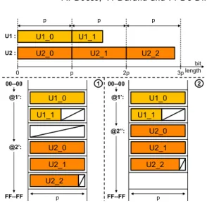
U2_0 U2_1 U2_2
U1_0 U1_1 p p 2p 3p 0 p p U2_1 U1_1 U1_0 p @2’’: @1’: U2_2 U2_1 U2_0 U1_1 U1_0 p U2 : U1 : bit length U2_0 U2_2 FF--FF 00--00 @2’: @1’: FF--FF 00--00 1 2
Figure 2: Variable length numbers in memory
2.1
Main memory organization of UNUM
array elements
In software applications, where iterations on arrays are per-formed, it is mandatory to preserve data locality in main memory, in order to guarantee affine accesses to random positions in compact arrays. Therefore, we assume that all el-ements of a compact array share the same memory footprint. Software applications which use compact UNUM arrays are affected by memory fragmentation and by arrays re-allocation. Those effects appear if a UNUM-array element changes its bit length after an operation. Array re-allocation requires expensive system calls. Figure 2 shows two memory addressing modes for UNUMs avoiding system calls usage.
The first one,○, aligns array’s elements on slots of p bits1
each. The number of slots must be sufficient to fit the array’s element maximum bit width. Hence the array’s element slot size (3p) and their address computation (@1’, @2’ ) are not data dependent and can be computed at compile time.
The second addressing mode○ concatenates the array2
elements in order to minimize the memory slots occupation. Arrays can not be overwritten (without re-allocation) and their access is sequential. Each load/store operation (in @1’ ) returns the address of the next element of the array (@2”). This addressing mode is only suitable for strictly sequential access and doesn’t allow, for instance, in-place updates of the array. For such situations, SMURF provides○.1
In○ and1 ○ the empty boxes (m) represent the unused2
bits in memory. Although○ wastes fewer bits than2 ○, it1
may not fully utilize the memory. To minimize this waste of bits, this work exploits the minimum usable granularity in the Rocketchip cache: p=8bits.
According to our experiments, FP algorithms which need precision are iterative. They generally tend to increase the length of their variables, thus in the end, the initially unused space in○ is eventually used.1
left right left right left right s u es-1 fs-1 s u es-1 fs-1 e e f f s u es-1 fs-1 e f 2 1 LSB MSB
Figure 3: Memory format for UNUMs and ubounds
2.2
Organization of the UNUM fields in
memory
For a UNUM/ubound which spans multiple addresses in a little-endian memory system (like RISC-V), it is important to have the descriptor fields present in the lower addresses. The conventional UNUM field organization (Figure 1, [7]) is not ideal since the position of the fixed length fields (u, es-1 and fs-1) changes according to the fields’ bit width.
Figure 3 depicts the adopted field organization for UNUM
1
○ and ubound○. In both formats, the fixed length fields2
(in green) are to the left of the variable length fields (in cyan and yellow). For ubounds○ the affinity with the left or right2
interval endpoint is noted above the fields.
This field organization is more convenient during load operations, because the fixed-length size fields are read first, so the size of the other fields is known early. Even when reading an ubounds○, the extraction of the fixed length and2
exponent fields can be done within one clock cycle with cheap hardware since their lengths, in the maximum supported Unum Environment (ess=4, fss=8), stays within 64 bits.
3
THE SMURF ARCHITECTURE
The SMURF coprocessor machine represents variable preci-sion Floating Point (FP) numbers in two different formats: internally the gbound (described below), in main memory UNUM/ubound. The conversion between these two formats is done on-the-fly by a dedicated load and store unit.
The coprocessor works with pointer-based computation: every access to scratchpad entries is done though pointers. The precision information is not encoded in dedicated instruc-tions but is carried by the data pointed in the scratchpad. In this way, the assembly code does not encode the format and can be reused after any precision reconfiguration.
The implementation as been parametrized so that many aspects (internal parallelism, maximum UE, register file size, etc.) can be customized based on the application. The set of parameters chosen in this article is as follows:
‚ 64 bit internal parallelism to be comparable to a 64-bit FPU;
‚ in memory, UE up to (4, 8) are supported (up to 256-bit fractions);
‚ a RF of 32 intervals (this number of registers matches the RISC-V ISA);
‚ in the RF, up to 512 bits of mantissa per interval endpoint.
All the results reported correspond to this set of parameters. The coprocessor architecture is pipelined with a fixed 64-bits internal parallelism. Each pipeline stage is based on
WGP = 2 gOP gRF[10] f eL 64 . 1 m0 m1 ··· mLmax f eL 64 . 1 m0 m1 ··· mLmax gRF[7] f eL 64 . 1 m0 m1 ··· mLmax f eL 64 . 1 m0 m1 ··· mLmax gRF[3] f eL 64 . 1 m0 m1 ··· mLmax f eL 64 . 1 m0 m1 ··· mLmax
Figure 4: WGP usage example
a stop-and-wait protocol to process the gbound mantissas divided in chunks (words [13]) of 64 bit each.
The coprocessor’s scratchpad has a gbound Register File (gRF) able to host 32 entries. Each entry (gbound) is made of two interval endpoints (gnumbers). Each endpoint has an header, and a mantissa. The mantissa is always normalized (hidden bit implicitly set) and it is divided into up to 8 chunks of 64 bits, for a maximum mantissa size of 512 bits. The header is made of sign, flags (NaN, 8, ...), exponent and length (L) fields. The L field encodes how many chunks are used (out of the available ones) to encode the mantissa.
The SMURF coprocessor has three internal Status Regis-ters (SR): DUE, SUE and WGP. The Default UNUM Environ-ment (DUE) SR stores the default UE used during load/store UNUM/ubound operations from/in the main memory.
The Secondary UNUM Environment (SUE) SR stores the secondary (optional) UE that can be used for UNUM-s/ubounds load/store operations from/in the main memory. Having two UE SRs (DUE and SUE) makes it possible to speedup UE conversion operations and to speedup load and store operations among different UEs.
The Working G-layer Precision (WGP) SR stores the max-imum precision (the number of 64-bit chunks in the mantissa) that the result of a coprocessor’s operation can have. Figure 4 depicts the WGP usage. A gbound operator (gOP) bounds the result’s output precision (L) at the value encoded in the WGP SR (2, sampled at instruction fetch).
4
THE SMURF ISA
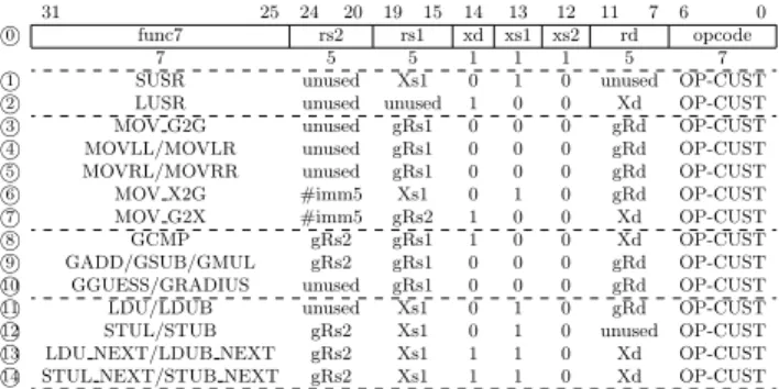
This Section introduces the Instruction Set Architecture (ISA) used to map the coprocessor instructions. Table 1 lists the encodings for the instructions used in the coprocessor. All these instructions are defined as an extension of the RISC-V ISA. The instruction field names are listed in ○. Those0
instructions are divided in four groups: internal Status Reg-ister (SR) settings (○-1 ○); mov operations (2 ○-3 ○); gbound7
operations (○-8 ○); load/store operations (10 ○-11 ○).14
4.1
Configuration instructions
SUSR○ sets the coprocessor status registers (DUE, SUE1
and WGP). The new values for the status registers are pushed inside the UNUM coprocessor through the General Purpose Register (GPR) of the RISC-V pointed by Xs1.
CoNGA’19, March 13–14, 2019, Singapore, Singapore A. Bocco, Y. Durand and F. De Dinechin 31 25 24 20 19 15 14 13 12 11 7 6 0 0 ○ func7 rs2 rs1 xd xs1 xs2 rd opcode 7 5 5 1 1 1 5 7 1
○ SUSR unused Xs1 0 1 0 unused OP-CUST
2
○ LUSR unused unused 1 0 0 Xd OP-CUST
3
○ MOV G2G unused gRs1 0 0 0 gRd OP-CUST
4
○ MOVLL/MOVLR unused gRs1 0 0 0 gRd OP-CUST
5
○ MOVRL/MOVRR unused gRs1 0 0 0 gRd OP-CUST
6
○ MOV X2G #imm5 Xs1 0 1 0 gRd OP-CUST
7
○ MOV G2X #imm5 gRs2 1 0 0 Xd OP-CUST
8
○ GCMP gRs2 gRs1 1 0 0 Xd OP-CUST
9
○ GADD/GSUB/GMUL gRs2 gRs1 0 0 0 gRd OP-CUST
10
○ GGUESS/GRADIUS unused gRs1 0 0 0 gRd OP-CUST
11
○ LDU/LDUB unused Xs1 0 1 0 gRd OP-CUST
12
○ STUL/STUB gRs2 Xs1 0 1 0 unused OP-CUST
13
○ LDU NEXT/LDUB NEXT gRs2 Xs1 1 1 0 Xd OP-CUST
14
○ STUL NEXT/STUB NEXT gRs2 Xs1 1 1 0 Xd OP-CUST
Table 1: Gbound computational instructions
LUSR○ loads the content of all the coprocessor SRs2
(DUE, SUE and WGP) into the GPR pointed by Xd. With this instruction the user can check if there is the need to change the internal coprocessor’s working precision. SUSR and LUSR do not implicitly reset the coprocessor.
4.2
Internal moves
MOV G2G○ copies the gbound content pointed by gRs13
in the one pointed by gRd.
MOVLL, MOVLR, MOVRL and MOVRR (○ and4 ○)5
copy the content of the gnumber (left for MOVLL and MOVLR, right for MOVRL and MOVRR) pointed by gRs1, in the gnumber (left for MOVLL and MOVRL, right for MOVLR and MOVRR) pointed by gRd.
MOV X2G○ copies the RISC-V’s GPR pointed by Xs1,6
in the #imm5-th word of the gbound pointed by gRd. MOV G2X○ copies of the #imm5-th word of the gbound7
pointed by gRs1, into the RISC-V’s GPR pointed by Xd. For MOV X2G and MOV G2X the #imm5 field is mandatory.
4.3
Internal arithmetic operations
GCMP ○ compares the gbounds pointed by gRs1 and8
gRs2 and stores all the comparison flags in the RISC-V’s GPR pointed by Xd. As specified in [7], the computed flags are: EQual (EQ), Not EQual (NEQ), Not Nowhere EQual (NNEQ), Greater Than (GT), Lower Than (LT). The user is responsible to program the RISC-V to parse those flags to make branch decisions.
GADD, GSUB, GMUL○ respectively add, subtract and9
multiply the gbounds pointed by gRs1 and gRs2 and store the result in the gbound pointed by gRd. In this release of the SMURF ISA the division is implemented in software.
GGUESS○ extracts the interval midpoint, rounded to10
the nearest even, of the gbound pointed by gRs1. The result p𝑜p𝑚𝑖𝑑q, 𝑜p𝑚𝑖𝑑qq is stored in duplicated form in the gbound pointed by gRd.
GRADIUS○ extracts the interval’s width of the gbound10
pointed by gRs1 and stores the result in the gbound pointed by gRd in the format p𝑤𝑖𝑑𝑡ℎ, 𝑤𝑖𝑑𝑡ℎq.
For GADD, GSUB, GMUL, GGUESS and GRADIUS operations, the output rounding precision (of the computed result) is defined in the WGP status register.
UNUM co-proc RoCC LSU RISC-V Rocket Chip FPU LSU $ L1 R A M Scratchpad $ L1 R A M 1 2 3 4 5
Figure 5: SMURF architecture overview
4.4
Load and store operations
Load and store operations support conversions between UNUM-s/ubounds in the main memory and scratchpad gbounds. The U2G and G2U subunits (Figure 6) support these conversions.
LDU/LDUB ○ load a UNUM/ubound stored in main11
memory at the address pointed by Xs1, converts it into the gbound format (with equal endpoints in case of UNUM), and stores the converted value in the gbound pointed by gRd.
STUL/STUB ○ stores the left gnumber, the gbound,12
pointed by gRs2, converted it in the UNUM/ubound for-mat, in main memory at address pointed by Xs1. All these operations use the UE defined in DUE.
Instructions LDU NEXT, LDUB NEXT, STUL NEXT, and STUB NEXT (○ and13 ○) implement the same function-14
alities of LDU, LDUB, STUL, and STUB respectively, and return the address of the next element in the main memory through Xd. They use the memory format described in Sec-tion 2.1. For LDU NEXT and LDUB NEXT the converted gbound is stored in the gbound pointed by gRs2.
Additional, dedicated load and store operations use the SUE SR. Their name is like○-11○ with a ‘ S’ at the end of14
the operation name: LDU S, LDUB S NEXT, etc.
5
SMURF MICRO-ARCHITECTURE
HARDWARE IMPLEMENTATION
The SMURF architecture is based on a RISC-V system gener-ated with the Rocketchip [3] design generator. We decided to use Rocketchip distribution because it supports coprocessors with dedicated ports to the RISC-V GPR and data cache, and it is possible to easily extend the RISC-V ISA while conserving GCC compiler support.
5.1
Overview of the system
Figure 5 depicts the SMURF architecture. The SMURF archi-tecture main core (RISC-V,○) is is connected to its native1
system: its 64 bits floating point unit (FPU), its memory hierarchy and its peripherals. The RoCC [12] interface○,2
provides the possibility to connect up to four coprocessors. This architecture only instantiates one coprocessor○.4
The coprocessor scratchpad hosts gbounds, and the main memory○ hosts UNUMs/ubounds. The conversion between5
those two formats is handled, during load and store opera-tions, by a dedicated Load and Store Unit (LSU,○).3
RoCC interface Instr. Data out Data In Memory Interface (cache L1) cw Control Unit gRF • 2 read ports • 1 write port • 32 VP g-bounds (64 g-numbers) d_cw gALU gop2 gop1 e_cw gres gres_dec gres_exe bus arbiter go p1 + g op 2 gre s gADD / gSUB gGUESS / gRADIUS gMUL gMOV gCMP gLSU G2U U2G Cache IF S R Left … f e L DW m1 mLmax . 1 m0 Right … f e L DW m1 mLmax . 1 m0 4 5 6 7 8 9 2 3 1
Figure 6: SMURF coprocessor pipeline
5.2
Coprocessor pipeline
Figure 6 depicts the SMURF coprocessor pipeline. It is based on 3 stages: decode○, execute1 ○ and write back2 ○. Stage3
synchronization barriers on the pipeline are denoted by ver-tical dashed lines¦. Fetch and memory stages are not needed. The instruction fetch is done by the main core as well as the address generation for the coprocessor’s LSU.
The coprocessor is interfaced, through the RoCC interface
4
○, with the main core (instructions and data ports) and with the memory (cache L1).
In○, the control unit1 ○ decodes the input instruction5
and generates the control words for the decode and execute stages.○ hosts the gbound Register File1 ○ (gRF, Section 3).6
The gRF has two read ports, one write port and hosts 32 Variable Precision (VP) gbounds with normalized mantissas.
The decode control word selects the gRF content (or the input data) that has to be propagated in the execute stage. The gRF controller○ keeps track of the running instructions6
and their data dependencies (e.g. read after write). In case of data dependency, the gRF controller sends to the main core a busy signal. This signal tells the main core whether the coprocessor is free to receive new instructions.
The coprocessor status registers○ (SR) are located be-7
tween the decode and the execute pipeline stages. SR contains the DUE, the SUE and the WGP status registers (Section 3). Their values are updated (or read) during the SUSR (or LUSR) operation (Section 3).
The execute stage hosts the arithmetic logic unit of the SMURF coprocessor ○. In8 ○ several pipelined operator8
units are instantiated to execute the ISA instructions pro-posed in Section 4. In this way independent operations can run in parallel either on different operators, or on differ-ent operator pipeline stages. The gMOV operator handles the MOV* instructions. The gCMP operator handles the GCMP instruction. The gMUL operator handles the GMUL instruction. The gADD operator handles the GADD, GSUB, GGUESS and GRADIUS instructions. The gLSU operator handles the LD*/ST* instructions, supporting the memory and field organizations introduced in Section 2.
STAGE
i-1 STAGEi STAGEi+1
ready valid ready valid BUFF … f e L DW m1 mLmax . m0 IB GB BUFF … f e L DW m1 mLmax . m0 IB GB FF-barrier FF-barrier
Figure 7: Coprocessor’s macro pipeline scheme
These operators○ receive operands and output results8
distributed on 64 bits chunks. The decode○ and write back7
time barriers have buses with 64 bits parallelism. All the operators which have operands/results on several mantissa chunks, have to require the input/output bus control to retrieve/write data from/into the gRF all the chunks.
Those requests are handled by the ‘bus arbiter’ units which ensure the correct data propagation among the pipeline. There are two bus arbiters: one which controls the decode buses, and one which controls the write back bus. Both are based on a stop and wait protocol. They receive the bus requests from the operators in○. Depending whether the8
buses are free or busy (taken by another operator), they give or deny the bus control through acknowledge signals. Once an operator takes control of the input (or output) bus, the coprocessor pipeline is stalled (the coprocessor is busy from the RISC-V perspective) until the bus request is revoked.
A multiplexer○ is used to provide to the main core either9
the gRF content, either gCMP operator result.
5.3
The macro-pipelined architecture
This work does internal Variable Precision (VP) mantissa computations with a fixed 64-bits data parallelism. This implies that mantissas operations are done iterating on man-tissas chunks. During these iterations the input manman-tissas chunks must be stored in internal buffers. We define macro-stage as the logic which iterates on mantissas chunks.
In the coprocessor pipelines, every mantissa operation requires a macro-stage. The pipeline macro-stages number is equal to the number of mantissa operations in it. The clock cycles latency of a macro-stage and the unit throughput are proportional and inversely proportional to the number of input mantissa chunks, respectively.
Figure 7 depicts the general scheme for each pipeline macro-stage (STAGE i). Each macro-macro-stage does a basic operation on mantissas (mov, addition, shift, leading zero count, ...). Each macro-stage is synchronized with others macro-stages through a ready-valid protocol. Each macro-stage is delimited by input/output synchronization stages.
Each synchronization stage is made of a buffer (BUFF) and a FF-barrier. FF-barriers host all the input/output infor-mation that are not part of a gnumber (e.g. the shift amount for the shift basic operation). Each buffer hosts a gnumber: a header, a memory to store the mantissa, integer bits (IB) and guard bits (GB). The header contains all the information
CoNGA’19, March 13–14, 2019, Singapore, Singapore A. Bocco, Y. Durand and F. De Dinechin
1
○ ○2 Area Total Power
Unit stg (𝜇𝑚2)○3 (𝜇𝑚2buff)○4 (mW )○5 (mW buff)○6
Rocket tile - 1553 (100%) n.a. (n.a.) 95.2 (100%) n.a. (n.a.)
–RISC-V - 23.09 (1.5%) n.a. (n.a.) 0.78 (0.8%) n.a. (n.a.)
–64bit fpu - 53.1 (3.4%) n.a. (n.a.) 1.43 (1.5%) n.a. (n.a.) –d cache - 487.6 (31.4%) n.a. (n.a.) 12.72 (13.4%) n.a. (n.a.) –i cache - 425.6 (27.4%) n.a. (n.a.) 8.51 (8.9%) n.a. (n.a.) –if/periph - 102.3 (6.6%) n.a. (n.a.) 3.83 (4.0%) n.a. (n.a.)
–coproc 3 461 (29.7%) 307 (66.5%) 17.0 (17.9%) 4.2 (24.7%) —s decode - 131.1 (8.4%) 130.3 (99.3%) 2.29 (2.4%) 2.16 (94.5%) —–gRF - 130.8 (8.4%) 130.3 (99.6%) 2.27 (2.4%) 2.16 (95.1%) —s execute - 327.5 (21.1%) 176.5 (53.9%) 13.6 (14.3%) 2.03 (14.9%) —–gMOV 1 4.242 (0.3%) 3.061 (72.2%) 0.17 (0.2%) 0.02 (14.1%) —–gCMP 3 30.73 (2.0%) 24.97 (81.3%) 0.83 (0.9%) 0.25 (29.9%) —–gADD 11 66.77 (4.3%) 43.61 (65.3%) 2.3 (2.4%) 0.42 (18.3%) —–gMUL 10 143.4 (9.2%) 60.06 (41.9%) 6.76 (7.1%) 0.98 (14.4%) —–gLSU 3 81.35 (5.2%) 44.77 (55.0%) 3.5 (3.7%) 0.36 (10.4%) ——LD 3 29.96 (1.9%) 16.95 (56.6%) 1.51 (1.6%) 0.14 (9.3%) ——–load 3 15.47 (1.0%) 9.344 (60.4%) 0.86 (0.9%) 0.08 (9.6%) ——–u2g 4 10.53 (0.7%) 4.579 (43.5%) 0.56 (0.6%) 0.04 (6.6%) ——ST 3 51.03 (3.3%) 27.81 (54.5%) 1.95 (2.0%) 0.22 (11.5%) ——–g2u 8 27.35 (1.8%) 16.96 (62.0%) 1.07 (1.1%) 0.11 (9.8%) ——–store 4 17.29 (1.1%) 10.84 (62.7%) 0.6 (0.6%) 0.09 (14.9%)
Table 2: SMURF architecture synthesis results
of the gnumber except the mantissa. In particular it contains the length field (L) which encodes the actual number of used chunks to express the mantissa. The size of the memory to host the mantissa is the maximum one supported by the gbound Register File (gRF). IB and GB are two additional fields that are used to add extra bits to the mantissa in order to do correct rounding during the FP algorithm. In particular, GB extends the last mantissa chunk (pointed by L).
An additional information required by each macro-stage is the result maximum output precision. This information is used to implement fused operations and to exploit the trade-off between latency and precision (WGB, Section 3).
With this architecture, the coprocessor macro-pipelines take care of the FP algorithm of each operator. The complex-ity to do operations on multiple mantissa chunks is pushed inside each pipeline macro stage. Since the coprocessor oper-ators support interval arithmetic, and interval endpoints run in parallel macro-pipelines, synchronization steps must be added to re-align the interval computation in the pipeline.
6
VALIDATION, FPGA INTEGRATION
AND SYNTHESIS
This section shows the techniques used to validate the design, its integration in FPGA, and its ASIC synthesis results.
6.1
Validation of the units
The SMURF architecture is validated at multiple levels start-ing from the basic components up to the top unit (Rocket tile). Each subunit is described in VHDL and is validated in simulation (with Questasim) against 50 millions pseudo random generated input vectors varying all the input param-eters. The output values of the units under test are compared with the ones generated by executable specifications written in high level behavioral VHDL code. A final validation test is done using a Xilinx Virtex 7 FPGA. Since an exhaustive vali-dation on FPGA of the whole SMURF architecture needs full compiler support for UNUMs, the final validation is based on
RISC-V 2% 64bit FPU 4% I cache 27% D cache 31% gMUL 9% gRF 9% gLSU 5% gADD 4% gCMP 2% others7% ASIC AREA [%] UNUM coproc: 29,7 % Rocket core + FPU: 4,9 %
Figure 8: Chip area distri-bution RISC-V 1% 64bit FPU 2% I cache 9% D cache 13% gMUL 7% gLSU 4% gRF 2% gADD 2% gCMP 1% clock tree 50% others 9% ASIC POWER [%] UNUM coproc: 17,9 % RISC-V + FPU: 2,3 %
Figure 9: Chip power distribution
calling hand-written instructions to check the correct inputs propagations into the coprocessor.
6.2
FPGA integration
The integration on FPGA is done through a microblaze system generated with Vivado from Xilinx. This system is a wrapper for the SMURF architecture. It connects the SMURF architecture to the DRAM and to a dedicated UART interface, both available on the FPGA board. The microblaze system is programmable through another UART interface. At boot, the microblaze loads the compiled code to be executed in the SMURF from a SD card into the DRAM. Once the DRAM contains the executable code for the RISC-V, the microblaze resets the SMURF module, then enters in sleep mode. With the reset, the SMURF module automatically starts to fetch the execution code from the DRAM. The produced outputs from the FPGA emulation are printed in a terminal connected to the SMURF UART interface.
The FPGA system can run at 50MHz. This frequency matches the Rocketchip specifications [3].
6.3
Synthesis results
The SMURF architecture (Section 5) was synthesized, us-ing Design Compiler from Synopsys, and targeted to ST’s 28nm FDSOI library (cmos028FDSOI). Register re-timing and clock gating optimizations are enabled during synthesis. For simplicity all the memory elements are synthesized with flip flops. The timing constraint is set at 1ns (1GHz ). To take into account connections external to the chip, a latency corresponding to the 70% of the clock cycle period is added to all the chip input/outputs. The debug input of the chip are disabled. The ‘flatten’ option of some sub units is disabled in order to be able to report area and power estimations after synthesis. The power estimation is done assuming a random switching activity on the inputs.
The best clock period achieved is 1.697ns (589MHz ). The critical path passes in the Floating Point (FP) multiply and add operator of the RISC-Vs FP unit.
Table 2 shows the synthesis results of the synthesized sys-tem. The Rocket tile is the name of the top unit. Column
1
○ lists the names of the synthesized components and sub-components units. Tabulations in this column denote the component hierarchy. Column ○ indicates the number of2
pipeline stages/macro-stages for each unit. Subcomponents not listed have 1 stage latency. Column ○ indicates the3
area of the unit expressed in 𝜇𝑚2. The percentages refer to the area taken by a unit compared to the one at the top (Rocket tile). Column○ depicts the area taken by mantissa4
buffers in the macro-pipeline for each unit (Section 5.3). The percentages refer to the area taken by the unit buffers (col-umn○) with respect to the one taken by each unit (column4
3
○). Column○ shows the power consumption required for5
each unit expressed in mW. Like for○, the percentages refer3
to the unit power consumption with respect to the one of the top. Column○, shows the power consumed by the interme-6
diate buffers of each unit expressed in mW. The percentages refer to the power consumption of the buffers with respect to the one of each unit. Figure 8 and Figure 9 depict the area and power distribution for some subunits.
From an area perspective the Rocket tile requires 1.5𝑚𝑚2
of silicon surface. The area takes into account the 50% of unused space for the place and route. The main contribu-tors of area footprint are the units which contain memory: instruction and data caches and the SMURF coprocessor. Columns○ and3 ○ show that the main area footprint con-4
tributors for the coprocessor are the units which contain memory: the gbound Register files and the macro-pipeline buffers. This is the hardware cost to have a pipelined high precision computation unit coprocessor.
In terms of power consumption the Rocket tile consumes 95mW. The biggest part of estimated power (47.5mW ) is consumed by the clock tree. The rest (47.6mW ) is consumed by the chip components. Like for the area, the main con-tributors for the power consumption are the instruction and data caches and the SMURF coprocessor. The unit which consumes more is the SMURF coprocessor with 17mW. One fourth of its power consumption is spent just in mantissa buffers and the rest is consumed in logic and standard flip flops. This high energy consumption is mostly due to the high number of pipeline stages of internal operators and by the additional logic of the finite state machines which handle multiple-chunk mantissa computations.
The SMURF coprocessor is 9 times bigger and consumes 12 times more than the RISC-V FP unit. However, the flops performance of this architecture is comparable to a regular fixed-precision IEEE FPU. That can be achieved due to its internal register file which is able to contain up to 32 intervals with 512 bits of mantissa precision for each endpoint. Furthermore the coprocessor requires fewer memory accesses compared to standard multiple precision software, due to few instructions being required per MPflops and the fact the internal register file containing up to 32 intervals with 512 bits of mantissa precision for each endpoint.
7
AN EXPERIMENTAL SOFTWARE
SETUP
Listing 1 shows, in C code, an experimental software setup ex-ample on the SMURF architecture. This exex-ample implement the division operation in the SMURF coprocessor using the
1 #include ” unum rocc . h”
2 void n r d i v i s i o n ( void ∗ res , void ∗op1 , void ∗op2 , int wgp) {
3 // Compute t h e Newton´Raphson r e c i p r o c a l 4 // ( 1 / op2 ) = Rn∗(2´(D∗Rn) ) 5 LDUB(G1 , op2 ) ; 6 LDUB(G5 , op1 ) ; 7 r e c i p r o c a l a p p r o x (G0 , G1) ; 8 f l o a t 2 g b o u n d (G2 , 2 . 0 , 4 , 8 ) ; 9 i n t i ; 10 f o r ( i =0; i <wgp ; i ++){ 11 GMUL(G3 , G1 , G0) ; // (D∗Rn) 12 GSUB(G4 , G2 , G3) ; //2´(D∗Rn) 13 GMUL(G0 , G0 , G4) ; //Rn∗(2´(D∗Rn) ) 14 } 15 // m u l t i p l y t h e r e c i p r o c a l w i t h op1 16 GMUL(G5 , G5 , G0) ; // op1∗(1/ op2 ) 17 STUB( r e s , G5) ; 18 } 19 i n t main ( ) 20 { 21 u b o u n d 4 8 t op1 , op2 , r e s ; 22 s e t d u e ( 4 , 8 ) ; 23 s e t s u e ( 4 , 8 ) ; 24 s e t w g p ( 7 ) ; 25 f l o a t 2 g b o u n d ( G10 , 2 . 0 , 4 , 8 ) ; 26 f l o a t 2 g b o u n d ( G11 , 3 . 0 , 4 , 8 ) ; 27 STUB(&op1 , G10 ) ; 28 STUB(&op2 , G11 ) ;
29 n r d i v i s i o n (& r e s , &op1 , &op2 , 7 ) ; 30 LDUB( G12 , &r e s ) ;
31 p r i n t g b o u n d ( G12 ) ; 32 return 0 ;
33 }
Listing 1: Example of division
ISA instructions listed in Section 4. This is not an optimized division algorithm but it shows how to write code for the coprocessor.
The unum rocc library (line 1) provides support for low-level programming simplifying the code development. It de-fines the unum ess fss t and ubound ess fss t types for each supported (ess,fss) Unum Environment (UE). These types map arrays of chars big enough to fit the maximum bit-length of the UNUM/ubound under its UE.
This library defines macros that map 1:1 all the ISA in-struction. These macros are expanded in in-line assembly instructions for the coprocessor. These in-line instructions are added in the RISC-V GCC compiler. This library defines the G0-31 constants to point to scratchpad gbounds.
The unum rocc library gives also support for some ba-sic functions. For example: reciprocal approx, (line 7) com-putes the first approximation for the Newton-Raphson (NR) division algorithm using the RISC-V FPU; float2gbound, (line 8) converts a 32bit float into gbound; set due, set sue
CoNGA’19, March 13–14, 2019, Singapore, Singapore A. Bocco, Y. Durand and F. De Dinechin
and set wgp (lines 22-24) set the coprocessor status regis-ters; print gbound (line 31) prints a gbound in the terminal through an FPGA’s UART interface.
The main function (line 19) sets the internal coprocessor status registers (lines 22-24), initializes the division operands and stores them in main memory in the ubound format (lines 25-28). Once the division is finished, it loads the computed result and prints its value on the terminal (line 30-31).
The division function (line 2) works for all the supported UEs. It divides two ubounds placed in main memory using the NR method and stores the result in memory at the specified address. First it computes the reciprocal of the divisor (lines 5-14), then multiplies it with the dividend (lines 16-17). The reciprocal of the divisor is computed from a first approximation (line 7), then the NR iteration is applied (lines 10-14). After the multiplication of the computed reciprocal with the dividend, the result is stored in memory.
The latency in a NR iteration varies between 33 (2 ˚ pp12` 1q ` p1 ˚ 9qq ` p1 ˚ 11q, one chunk) and 362 (2 ˚ pp82` 1q ` p8 ˚ 9qq ` p8 ˚ 11q, eight chunks) clock cycles. At 600 MHz these latencies correspond to a performance which varies between 54 and 5 Mflops. The RISC-V FPU running the same code on 64 bit floats, hypothesizing a latency of three clock cycles per FPU operation, has a performance at 600MHz of 200Mflops. State-of-the-art multiple-precision software such as GMP and MPFR have not yet been ported to RISC-V. However, extrapolating their performance on a standard PC, we expect that MPFR can compute both 512-bit accuracy interval end-points at about 1Mflops at 600MHz. The proposed accelerator therefore offers 5x performance with the same flexibility.
8
CONCLUSION AND FUTURE WORK
This work proposes a Variable Precision (VP) Floating Point (FP) accelerator (SMURF) based on RISC-V ISA (Instruction Set Architecture) for high performance computing servers as an alternative to VP FP software routines (e.g. [4]). The SMURF accelerator is implemented as a coprocessor of a RISC-V processor generated with the Rocket-chip genera-tor [3]. All the coprocessor features are exposed to the user expanding the RISC-V ISA.
The coprocessor works with two FP formats: one dedicated to the main memory (UNUM/ubound) and the other to the internal computations (gbound). In main memory, the coprocessor supports several Unum Environments (UE [7]) up to 16 and 256 bits of exponent and mantissa. Internally, the coprocessor supports fused operations on the numbers hosted in the internal register file (gRF) which can contain 32 intervals with 512 bits of mantissa per interval endpoint. The coprocessor architecture is pipelined with a fixed internal parallelism of 64 bits. The coprocessor has pipelined operators and a dedicated Load and Store Unit (LSU) which handles the conversions between memory and internal VP FP formats. The support of VP mantissas (512 bits) with a fixed internal parallelism (64 bit) requires intermediate mantissa buffers and finite state machines in all the pipeline stages.
The area footprint and the power consumption of the coprocessor is respectively 9 and 12 times higher than the ones of the RISC-V 64 bits FP unit. The large area footprint of the coprocessor is due to the large usage of internal memory elements (gRF and pipeline buffers). The coprocessor power consumption is dissipated mainly in the mantissa buffers and in the internal logic to handle VP mantissas.
However, the flops performance of this architecture stays within the range of a regular fixed-precision IEEE FPU. More-over, the UNUM format allows to exploit interval arithmetic in real applications having variable memory footprint data. The next steps of this work are: optimize the co-processor pipeline and operator units; embed additional operators (e.g. the division); support scalar computation; explore other float-ing point formats; provide compiler support for high-level programming and evaluate computational performances on real scientific computing applications.
REFERENCES
[1] A. Bocco, Y. Durand, and F. de Dinechin. 2017. Hardware
support for UNUM floating point arithmetic. In Ph.D.
Re-search in Microelectronics and Electronics. 93–96. https:
//doi.org/10.1109/PRIME.2017.7974115
[2] Cohen, Hull, and Hamacher. 1983. CADAC: A
Controlled-Precision Decimal Arithmetic Unit. IEEE Trans. Comput. C-32, 4
(April 1983), 370–377. https://doi.org/10.1109/TC.1983.1676238
[3] Asanovi´c Krste et al. 2016. The Rocket Chip Generator.
Techni-cal Report UCB/EECS-2016-17. EECS Department, University
of California, Berkeley. http://www2.eecs.berkeley.edu/Pubs/
TechRpts/2016/EECS-2016-17.html
[4] Laurent Fousse, Guillaume Hanrot, Vincent Lef`evre, Patrick
P´elissier, and Paul Zimmermann. 2007. MPFR: A
Multiple-precision Binary Floating-point Library with Correct Round-ing. ACM Trans. Math. Softw. 33, 2, Article 13 (June 2007). https://doi.org/10.1145/1236463.1236468
[5] F. Glaser, S. Mach, A. Rahimi, F. K. G¨urkaynak, Q. Huang, and
L. Benini. 2018. An 826 MOPS, 210uW/MHz Unum ALU in 65 nm. In International Symposium on Circuits and Systems. 1–5. https://doi.org/10.1109/ISCAS.2018.8351546
[6] Torbj¨orn Granlund and the GMP development team. 2012. GNU
MP: The GNU Multiple Precision Arithmetic Library. https:
//gmplib.org/ Version 5.0.5.
[7] John L. Gustafson. 2015. The End of Error: Unum Computing. Chapman and Hall/CRC.
[8] J. Hou, Y. Zhu, Y. Shen, M. Li, H. Wu, and H. Song. 2017. Tackling Gaps in Floating-Point Arithmetic: Unum Arithmetic Implementation on FPGA. In High Performance
Comput-ing and Communications. 615–616. https://doi.org/10.1109/
HPCC-SmartCity-DSS.2017.82
[9] T. E. Hull, M. S. Cohen, and C. B. Hall. 1991. Specifications for a variable-precision arithmetic coprocessor. In Proceedings 10th
IEEE Symposium on Computer Arithmetic. 127–131. https:
//doi.org/10.1109/ARITH.1991.145548
[10] IEEE754-2008 2008. IEEE Standard for Floating-Point Arithmetic.
IEEE 754-2008, also ISO/IEC/IEEE 60559:2011. https://doi.
org/10.1109/IEEESTD.2008.4610935
[11] Ulirich Kulisch. 2013. Computer arithmetic and validity: Theory, implementation, and applications, 2nd edition. De Gruyter.
[12] Anuj Rao. [n. d.]. The RoCC Doc V2: An
Introduc-tion to the Rocket Custom Coprocessor Interface. ([n.
d.]). https://docs.google.com/document/d/1CH2ep4YcL
ojsa3BVHEW-uwcKh1FlFTjH kg5v8bxVw
[13] M. J. Schulte and E. E. Swartzlander. 2000. A family of variable-precision interval arithmetic processors. IEEE Trans. Comput.


![Figure 8: Chip area distri- distri-bution RISC-V64bit FPU1%2% I cache D cache9%13%gMUL7%gLSU4%gRFgADD2%2%gCMP1%clock tree50%others9%ASIC POWER [%] UNUM coproc:17,9 %RISC-V+FPU:2,3 %](https://thumb-eu.123doks.com/thumbv2/123doknet/12990085.379188/7.918.81.441.124.387/figure-distri-distri-bution-grfgadd-others-power-coproc.webp)
