HAL Id: hal-02474577
https://hal.archives-ouvertes.fr/hal-02474577
Submitted on 23 Mar 2020
HAL is a multi-disciplinary open access
archive for the deposit and dissemination of sci-entific research documents, whether they are pub-lished or not. The documents may come from teaching and research institutions in France or abroad, or from public or private research centers.
L’archive ouverte pluridisciplinaire HAL, est destinée au dépôt et à la diffusion de documents scientifiques de niveau recherche, publiés ou non, émanant des établissements d’enseignement et de recherche français ou étrangers, des laboratoires publics ou privés.
Annealing impact on emission and phase varying of
Nd-doped Si-rich-HfO2 films prepared by RF magnetron
sputtering
T. Torchynska, L. Vega Macotela, L. Khomenkova, F. Gourbilleau, L.
Lartundo Rojas
To cite this version:
T. Torchynska, L. Vega Macotela, L. Khomenkova, F. Gourbilleau, L. Lartundo Rojas. Annealing im-pact on emission and phase varying of Nd-doped Si-rich-HfO2 films prepared by RF magnetron sput-tering. Journal of Materials Science: Materials in Electronics, Springer Verlag, 2020, �10.1007/s10854-020-03010-9�. �hal-02474577�
Annealing impact on emission and phase varying of Nd‑doped
Si‑rich‑HfO
2films prepared by RF magnetron sputtering
T. Torchynska · L. G. Vega Macotela · L. Khomenkova · F. Gourbilleau · L. Lartundo Rojas
Abstract
HfO2 films doped with Nd and Si atoms were produced by RF magnetron sputtering in argon plasma atmosphere. The effect of annealing treatment on the morphology, crystal structure and light emission of the films was investigated by means of the scanning electronic microscopy (SEM), energy dispersive X-ray spectroscopy (EDS), X-ray diffraction (XRD), photolumi-nescence (PL) and X-ray photoelectron spectroscopy (XPS). The thermal treatment was performed in the temperature range of TA = 800–1100 °C in horizontal furnace with continuous nitrogen flow. For annealed Si–HfO2:Nd films, the SEM study revealed the formation of the grains with the mean size of about 20–60 nm that show the tendency to enlarge with the TA rise. Besides, the phase separation was observed and tetragonal HfO2 and SiO2 phases were detected by the XRD method for the films annealed at TA > 950 °C. The PL study revealed that both Nd3+ ions and host defects contribute to PL emission whereas their relative contribution depends on the TA and on the crystal phase of host matrix. The highest PL intensity of Nd3+ ions via 4f inner electronic shell levels was detected for T
A = 950 °C. The variation of PL intensity of Nd3+ ions was correlated with the change of PL intensity of the band caused by the host defects. These latter participate in the energy transfer towards Nd3+ ions. This statement was confirmed by XPS data, as well as by the shape of PL spectra. It was shown that the bright emission via Nd3+ ions can be achieved for those located in the tetragonal HfO
2 matrix.
1 Introduction
Hafnium dioxide (HfO2) is interesting material for different applications. In nuclear industry this oxide can be used as the high temperature or high pressure materials. In elec-tronics it competes with silicon oxide as the gate oxide or material for optical waveguides [1–4]. The advances of HfO2 parameters are the extreme chemical inertness, high melting
temperature and high cross-section for thermal neutron cap-ture [1]. The recent interest to hafnium dioxide was con-nected with its using as complementary metal-oxide semi-conductor (CMOS) in integrated circuits due to its higher dielectric constant (k) important for the gate oxides [3, 4]. Other advantages of hafnium dioxide are the large conduc-tion band offset (1.5 eV) and compatibility with polysilicon gate technology [5, 6].
It is worth to note that the HfO2-based compounds were not well addressed early as a matrix for the rare-earth ions. Few groups only reported on the light emission obtained from Eu3+-doped HfO
2 nanotubes [7], Er3+-doped sol–gel SiO2–HfO2 waveguides [8, 9], and Nd3+, Er3+ or Pr3+ doped HfO2 films [10–13].
Earlier, the interest to neodymium (Nd3+) ions has been caused by their application in inorganic laser materials. Nd3+ ions exhibit the broad absorption at 800 nm and intense emission in the IR range from 0.80 to 1.43 μm connected with a set of the 4F
3/2 → 4IJ (J = 9/2, 11/2, 13/2) optical tran-sitions in the 4f electronic shell [14, 15].
The previous study of Si-rich HfO2 films co-doped with rare-earth ions [10, 11] showed that the bright photolumines-cence (PL) in visible and infrared spectral ranges, related to
the rare-earth ions, can be obtained from the films annealed either at 900–950 °C [10] or at 950–1050 °C [11]. The rea-sons of this phenomenon were unclear and required addi-tional study. Moreover, the chemical bonding of Hf, Si, O and rare-earth ions was not analyzed. In this paper, we report on the investigation of PL emission and crystal structure of Si-rich HfO2 films doped with Nd ions grown by radio frequency (RF) magnetron sputtering. The phase separation process in these films induced by thermal treatment was con-trolled by means of X-ray diffraction (XRD) method. To understand the impact of thermal treatments on the Nd ion surrounding, the X-ray photoelectron spectroscopy (XPS) was used.
2 Experimental details
The films were grown by RF magnetron sputtering on the 2-inch, B-doped, (100) oriented Si wafers with a resistivity of 15 Ω cm. Prior to deposition, the substrates were submit-ted to standard RCA cleaning, dipped in 10% HF solution, rinsed in distilled water and dried in nitrogen flow. After this, the substrates were place immediately in load-lock of deposition unit. The HfO2 target (99.9% Testbourn Ltd.), topped with the calibrated 1 cm2 Si and Nd
2O3 pellets that covered of 16% target surface each, was used. The growth of Si–HfO2:Nd films was carried out in pure Ar plasma with the argon flow (fAr = 3 sccm). The RF power, substrate tempera-ture, plasma pressure and substrate-cathode distance were 0.74 W/cm2, 400 °C, 0.03 mbar and 57 mm, respectively. The deposition time was about 200 min allowed growing of homogeneous films with the 410-nm thickness. After depo-sition, the substrate with the film was cut on the pieces with the dimensions of 1 × 1 cm2 (so-called as samples) to study the effect of different annealing temperatures. Annealing treatment was carried out in a conventional horizontal fur-nace at the temperatures TA = 800–1100 °C for tA = 15 min in continuous nitrogen flow (48 sccm). For this purpose, the samples were placed in the cold zone of the furnace and kept there during 15 min in continuous nitrogen flow. Then (under continuous nitrogen flow), they were transferred in the hot zone of the furnace and annealed there during 15 min. After annealing, the samples were extracted from the hot zone and cooled down to room temperature in nitro-gen flow. The heating and cooling rates were about 45 °C/s. To study the surface morphology, as well as to obtain the information on film chemical composition, a scanning electronic microscope (SEM) Quanta 3D FEG-FEI with a detector Apollo X10 mark EDAX for the X-ray energy dis-persive spectroscopy (EDS) was used.
X-ray diffraction (XRD) patterns were recorded at the symmetric geometry on Model X” PERT MRD equipment with a Pixel detector, three axis goniometry and parallel
collimator, with the angular resolution of 0.0001°. X-ray beam was from the Cu source (K1 line, λ = 1.5406 Å).
PL spectra were recorded in the 400–1000 nm spectral range using a Jobin–Yvon TRIAX 180 monochromator with a Hamamatsu E717-500 PMT Socket Assembly and a SRS lock-in amplifier (SP830 DPS) and in 800–1500 nm spectral range using Jobin THR 1000 monochromator with Hama-matsu C9940-02 PMT Cooled Housing and a SRS lock-in amplifier (SP830 DPS).
To detect the chemical compositions of the films as well as Nd ion surrounding, the X-ray photoelectron spectros-copy (XPS) has been realized on the Thermo Scientific™ K-Alpha™ XPS spectrometer operated at 15 kV (90 W) at a pressure of 1.33 × 10⁻⁷ Pa. In this case, the Al K
a radiation (with energy of 1486.7 eV) was used. The X-ray beam of 400 µm cross-section was applied in two pass energy modes of 160 and 40 eV. To analyze the XPS spectrum, the Thermo Avantage V5.938 software was applied. All experiments were carried out at 300 K.
3 Results and discussion
3.1 Surface morphology and chemical composition
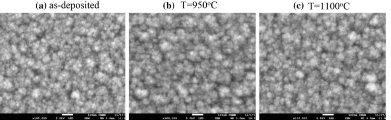
Figure 1 shows the SEM images of as-deposited (AD) and annealed Si–HfO2:Nd films. The surface of AD films shows the presence of the grains with the sizes of 20–60 nm (Fig. 1a). The grain sizes increase up to 40–100 nm after film annealing at 950 and 1100 °C (Fig. 1b, c). The last effect is connected with the crystallization process occurred at high temperatures.
The film composition analyzed by the EDS technique is shown in Fig. 2. In all films, the Hf, Si, O, N and Nd ele-ments were detected. The O signal enlarges significantly with increasing the annealing temperature (Fig. 2a). The O and N signal variation after annealing can be owing to the surface adsorption of these elements from an annealing atmosphere and then their diffusion into the films.
3.2 XRD study
The XRD patterns of Si–HfO2:Nd films are shown in Fig. 3. The AD film demonstrates XRD peaks (Fig. 3, curves 1) that can be attributed to the different phases. The high intensity XRD peak at 2Θ = 69.173° (f) is identified as XRD signal from the (400) planes in cubic Si crystal structure (ICSD Ref. code 00-005-0490). This signal is related to the Si substrate.
XRD peaks with the small intensity (Fig. 3, curves 1) detected at 2Θ = 35.595° (b), 56.372° (c) and 69.231° (g) are assigned to the X-ray diffraction from the (112), (213) and (204) planes, respectively, in the tetragonal
HfSiO4 phase (ICSD Ref. code 00-008-0345). Mean-while, the XRD peaks at 2Θ = 61.632° (d) and 66.215° (e) were attributed to the diffraction from the (241) and (338) planes in the tetragonal Nd2Si2O7phase (ICSD Ref.
code 01-089-5347). It is supposed that the appearance of tetragonal HfSiO4 and Nd2Si2O7 phases can be favored in AD films by high enough substrate temperature (400 °C).
Fig. 1 SEM images of Si–HfO2:Nd films as-deposited (a) and annealed at 950 (b) and 1100 °C (c)
0.2 0.4 0.6 0.8
1100 oC
950 oC
Normalized EDS signal, arb.un
Energy, keV OKα HfO Hf N NKα (a) (b) AD 1.0 1.2 1.4 1.6 1.8 2.0
Normalized EDS signal, arb.un.
Energy, keV NdM HfM SiKα NdM 1100 oC 950 oC AD
Fig. 2 EDS spectra of Si–HfO2:Nd films: as-deposited (curve 1) and
annealed at 950 (curve 2) and 1100 °C (curve 3)
100 1000 10000 100 1000 20 30 40 50 60 70 80 90 100 1000 1100°C g f b c d e 1 4b 1 2a 4a 6a 7 3 2b 3 5 6b 1 2a 3 6a 4 5 2 7 2b 6b XRD Intensity (Counts) 950°C
θ/2θ
(degree) ADFig. 3 XRD spectra of Si-HfO2:Nd films: as-deposited (curve 1) and
Annealing the Si–HfO2:Nd film at TA = 950 °C stimu-lates structure variation (Fig. 3, curve 2). The XRD signals from Nd2Si2O7 and HfSiO4 tetragonal phases disappeared (Fig. 3, curve 2) that can be connected with the decomposi-tion of both these phases. At the same time, the XRD peaks connected with the tetragonal HfO2 phase were detected at 2Θ = 30.052° (1), 34.812° (2a), 35.052° (2b), 50.452° (3), 59.952° (4), 61.936° (5) and 82.452° (7) (Fig. 3, curve 2). These peaks are related to the (112), (002), (200), (220), (311), (222) and (204) planes in the tetragonal HfO2 phase (ICSD Ref. code 00-008-0342), respectively. Addition-ally, the peak 6a shifts towards 2Θ = 69.272° (6a) due to its overlapping with the XRD peak at 2Θ = 70.603° (peak 6b) (Fig. 3, curve 2). The last one can be assigned to the X-ray diffraction from a (002) plane in the tetragonal SiO2 phase (ICSD Ref. code 00-045-1374).
Annealing at TA = 1100 °C did not change significantly the XRD pattern of the Si–HfO2:Nd film (Fig. 3, curve 3) and all XRD peaks related to the tetragonal HfO2 phase can be seen clearly. The peak intensities increase and their full width at half maximum (FWHM) decreases. The last fact testifies to enlarging the HfO2 nanocrystal sizes. The nanocrystal sizes (coherent domain sizes) estimated using the Scherrer’s formula from the XRD peaks related to the tetragonal HfO2 were 5 nm and 8 nm after annealing at 950 and 1100 °C, respectively.
Furthermore, the first XRD peak 30.052° shifted to 30.192° and the small intensity XRD peaks (4b, 5, 6b) appeared after annealing at TA = 1100 °C (Fig. 3, curve 3). Annealing at higher temperatures (1000–1100 °C) stimulates the silicon oxide crystallization in the studied films that is accompanied by appearing the other set of XRD peaks at 2Θ = 30.192° (1), 56.372° (5), 60.472° (4b) and 70.603° (6b) corresponded to the (110), (121), (066) and (002) planes in the tetragonal SiO2 phase (ICSD Ref. code 00-045-1374).
3.3 PL study
PL spectra of as-deposited and annealed Si–HfO2:Nd films are shown in Fig. 4. The total PL intensity increases sig-nificantly after annealing at 950 °C, but it changes slightly after annealing at 1100 °C in comparison with the AD state (Fig. 4). PL spectra consist of several PL bands related to the optical transition in the 4f inner electronic shell of Nd3+ ions with the peaks (1–10) in the spectral range of 350–1500 nm (Fig. 4, Table 1). Additionally, the PL peak X has been detected and assigned to emission via native host defects (Fig. 4, Table 1). The comparison of PL spectra shows that increasing the PL intensity and its decreasing correlate with varying the PL intensity of the band X in Fig. 4. It is clear that the contribution of Nd3+ ions and host defects in film emission depends on annealing temperatures and on the crystal phase of host matrix (Table 1, Fig. 4).
0.0 5.0E2 1.0E3 1.5E3 0 1E4 2E4 3E4 4E4 5E4 400 500 600 700 800 900 0.0 5.0E2 1.0E3 1.5E3 PL intensity, arb. un . 1100 °C a b cd 3 4 5 e 7 f 8 9 10 300K
c
950 °C 1 2 3 X 4 5 6 7 89 10 300Kb
Wavelngth (nm) AD 300Ka
800 1000 1200 14000
2
4
6
8
10
12
14
1100
oC
950
oC
PL intensity, arb. un
.
Wavelength, nm
AD
(a) (b)Fig. 4 PL spectra of Si-HfO2:Nd films: as-deposited and annealed at
950 and 1100 °C recorded in the visible (a) and infrared (b) spectral ranges
4591
It was shown early that the emission of pure HfO2 is char-acterized by the PL bands in the ultraviolet (4.0–4.2 eV) and visible (2.2–3.5 eV) spectral ranges [10, 11]. The UV emission was attributed either to the emission of the self-trapped exciton or to oxygen vacancies. Since the exciton emission is usually quenched to 300 K, the most probable center for UV emission are oxygen vacancies (Fig. 4a). Along with this, visible emission at 300 K was attributed to the carrier recombination via oxygen vacancies with trapped electrons [10, 11]. In present study, the band X centered at 555 nm (≈ 2.23 eV), which appeared after annealing at
950 °C (Fig. 4b), can be attributed to the optical transitions via different types of oxygen vacancies. The film oxidation while annealing at 1100 °C reduces the number of oxygen vacancies in the films and, as result, the PL intensities of the band X and all PL bands related to the recombination via Nd ions fall down in the PL spectrum (Fig. 4).
The native defects can influent on the excitation of rare-earth ions in the films. It is known that the absorption cross-section of rare-earth ions for 4f–4f transitions is about 10−19–10−21 cm−2 and require a high power for the direct excitation [16–18]. It was shown early that the host-mediated excitation of 4f–4f transitions can be very effective owing to. the excitation energy transfer. In this case, the high intensity of Nd3+ related PL bands (Fig. 4b) can be assigned to the efficient interaction of host defects, oxygen vacancies [19,
20], with Nd3+ ions. To confirm this conclusion, the XPS spectra of studied films were investigated.
3.4 XPS study
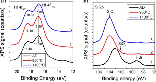
XPS spectra of Si-HfO2:Nd films measured in the high reso-lution mode for the AD film and after annealing at 950 and 1100 °C are shown in Figs. 5 and 6. The four XPS lines related to Hf 4f, Si 2p, O1s and Nd 3d have been monitored.
For as-deposited film, the XPS spectra showed the Hf doublet: Hf 4f5/2 and Hf 4f7/2 peaked at 18.48 and 16.98 eV, respectively, which are typical for the Hf–O bonds in haf-nium oxide [21–23]. Additionally, the small intensity XPS peak is detected at 13.58 eV that can be attributed to the Hf 4f7/2 line in the metallic hafnium [21].
The XPS peaks of the main Hf 4f doublet did not change their positions after film annealing at 950 °C (Fig. 5a), whereas a small shift of these XPS peaks toward lower binding energies was found for the film annealed at 1100 °C (Fig. 5a). Moreover, the small XPS peak at 13.58 eV disap-peared after annealing at 950 °C and the intensity of the
Table 1 Optical transitions detected in the films (Fig. 4) Number Wavelength
(nm) Optical transition References
TA = 950 °C 1 400 4P 3/2 → 4I9∕2,2P1/2 → 4I9∕2 [19] 2 455 4G 11/2 → 4I9∕2,4G9/2 → 4I9∕2 [19] 3 530 4G 7/2 → 4I9∕2 [13] X 555 VO [10,11] 4 605 2G 7/2 → 4I9∕2 [11] 5 660 4F 9∕2 → 4I9∕2 [15] 6 710 4F 7∕2 → 4I9∕2 [15] 7 730 4S3∕2 → 4I9∕2 [15] 8 780 4F5∕2 → 4I9∕2 [15] 9 800 4H 7/2 → 4I9∕2 [15] 10 885 4F 3∕2 → 4I9∕2 [14,19] TA = 1100 °C a 390 4P 3/2 → 4I9∕2 [15] b 420 2P1/2 → 4I9∕2 [15] c 455 4G11/2 → 4I9∕2 [13] d 475 4G9/2 → 4I9∕2 [19] e 625 4H11∕2 → 4I9∕2 [13] f 760 4H 9/2 → 4I9∕2 [15]
Fig. 5 High resolution XPS spectra of Hf 4f (a) and Si 2p (b) lines of Si-HfO2:Nd films:
as-deposited (curve 1) and annealed at 950 (curve 2) and 1100 °C (curve 3)
20 18 16 14 12
XPS signal (counts/s)
Binding Energy (eV)
AD 950°C 1100°C Hf 4f 7/2 Hf 4f5/2 1 2 3 16.98 18.48 16.88 16.98 18.48 18.38 106 104 102 100 98 96 XPS signal (counts/s)Binding energy (eV) AD 950°C 1100°C Si 2p SiO2 SiOx Si 1 2 3 (a) (b)
main Hf 4f doublet increased. Thus, an annealing stimu-lated pronounced formation of Hf–O bonds with Hf4+ charge state (corresponded to Hf charge state in HfO2 phase). This occurs via additional oxidation of metallic Hf (reflected by the change of Hf ion charges from Hfo in metallic hafnium to Hf4+ in HfO
2) and/or via HfSiOx phase separation and formation of HfO2 phase.
However, the crystallization process that takes place in hafnium oxide at 950 °C did not affect the peak positions of main Hf 4f doublet. Meanwhile, the small shift of Hf 4f doublet peaks to lower binding energies after annealing at 1100 °C may be connected with the effective Si oxidation and formation of tetragonal SiO2 phase that leads to some destruction of the hafnium oxide phase.
Two XPS peaks at 99.18 eV and 103.08 eV, related to the Si 2p3/2 line, are detected for the AD state of Si–HfO2:Nd film (Fig. 5b). The peak at 99.18 eV is connected with the silicon nanocrystals (NC) in Si–HfO2:Nd films [21]. The second peak at 103.08 eV can be attributed to the Si2+ ions in silicon suboxide, SiOx [21, 22]. Si NC oxidation at higher temperatures leads to disappearing the XPS peak at 99.18 eV. Simultaneously, the XPS intensity of high binding energy Si 2p peak increases and it shifts to 104.08 eV. This last peak position corresponds the Si 2p3/2 line of Si4+ions in silicon dioxide, SiO2 [21].
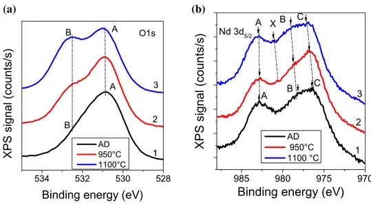
High resolution XPS spectra of the oxygen O1s line in the Si–HfO2:Nd films are presented in Fig. 6a. In the AD state only one asymmetric XPS peak has been detected at 530.88 eV (Fig. 6a). The last peak can be attributed to the Hf–O bonds in the Si–HfO2:Nd films [24, 25]. This peak position in XPS spectra does not change after annealing at 950 °C, but shifts to 530.98 eV after annealing at 1100 °C (Fig. 6a). Simulta-neously, the thermal treatment stimulates the growth of the second oxygen XPS peak at 532.28 eV. Note, that the second O1s peak appearing at high temperature correlates with the Si
oxidation upon annealing. This XPS peak at 532.28 eV can be attributed to the Si–O bonds in silicon oxides [21]. It is worth to note that the constant position of the first O1s XPS peak (530.88 eV) in hafnium oxide after annealing at 950 °C corre-lates with the constant position of the main Hf 4f doublets after this annealing. It means that short ordering of Hf–O bonds in the hafnium oxide varies a little upon the crystallization of this phase during annealing.
High resolution XPS spectra of Nd 3d lines are presented in Fig. 6b. XPS spectra permit to detect the Nd 3d5/2 peak (A) at 982.5 eV in the AD film state that, as a rule, is attributed to the Nd3+ions in neodymium oxide (Nd
2O3) [22–25]. Additionally, in XPS spectra of Nd3d lines two other overlapped peaks B and C located at 978.08 eV (B) and 976.48 eV (C), respec-tively, can be seen. The shift of Nd 3d peaks to lower binding energies, in comparison with the Nd3+ion peak at 982.5 eV, permits to suppose that B and C peaks belong to the Nd ions with other charges [24, 25]. The analysis of published results has summarized in Table 2, where the peak positions of Nd 3d5/2 lines are shown for the different Nd ion charge states. Presented analysis permits to assign the XPS peaks B and C to Nd1+and Nd0 states. The appearance of Nd atoms with the charge states Nd0 and Nd1+ may be owing to their insufficient oxidation at the film growth in Ar atmosphere.
The film thermal treatment at 950 °C leads to the preferen-tial growth of the peak B and C intensities and their shift to the higher binding energies of 978.68 eV (B) and 976.78 eV (C) that again testifies to insufficient oxidation the Nd atoms and,
Fig. 6 High resolution XPS spectra of O1s (a) and Nd 3d (b) lines of Si-HfO2:Nd films:
as-deposited (curve 1) and annealed at 950 (curve 2) and 1100 °C (curve 3)
534 532 530 528
XPS signal (counts/s
)
Binding energy (eV) AD 950°C 1100°C O1s A A B B 1 2 3 985 980 975 970
XPS signal (counts/s)
Binding energy (eV)
AD 950°C 1100 °C Nd 3d5/2A B C 1 2 3 A B C X (a) (b)Table 2 Binding energy of Nd 3d5/2 peaks for different charge states
of Nd ion
Nd 3d5/2 lines Nd0 Nd1+ Nd2+ Nd3+ References
4593
as consequence, the lack of oxygen in the HfO2 matrix. It is clear that this situation is favorable for the high concentration of oxygen vacancies in the host HfO2 matrix, which are nec-essary for the energy transfer from host defects to Nd ions at the efficient Nd ion excitation (Fig. 7). Meanwhile, annealing at 1100 °C stimulates the efficient oxidation and preferential growth of the peak A intensity that related to the Nd3+ions in neodymium oxide. Simultaneously, the peaks B and C con-tinue shifting to higher binding energies of 978.98 eV (B) and 977.08 eV(C) and the new small peak X appearing. The last one can be attributed to the Nd2+ ion states. Thus, all men-tioned features in varying the Nd 3d5/2 peaks are connected with efficient oxidation of Nd atoms at higher temperature annealing. Furthermore, the variation of Nd 3d5/2 peaks with annealing permits to confirm that for the bright emission via Nd ions is necessary the insufficient oxidation of Nd ions and the host HfO2 matrix. The effect of decreasing the PL intensity of deep level emission bands after annealing in oxygen atmos-phere was detected in the ZnO:Gd films early [26].
4 Conclusions
The effects of annealing conditions on the phase chemical compositions and crystal structure of the Si–HfO2:Nd films have been studied. The correlation between the bright emis-sion via the 4f inner electronic shell of Nd ions and the high intensity of PL band X, related to emission via the oxy-gen vacancies in the host HfO2 matrix, has been revealed. The XPS study, additionally, confirms that for the bright
emission via Nd ions is necessary the insufficient oxida-tion of Nd ions and the host tetragonal HfO2 matrix. This condition is favored for the high concentration of oxygen vacancies in the HfO2 films that is necessary for the efficient energy transfer toward Nd ions.
Acknowledgements This work was supported by the National Acad-emy of Sciences of Ukraine (Project III-4-16), Ministry of Educa-tion and Science of Ukraine (Project ID: 89452), the French NaEduca-tional Agency of Research (ANR), as well as by CONACYT Mexico (Grant 258224) and SIP-IPN Mexico (20195080).
References
1. Komarek, K.L., Spencer, P.J., International Atomic Energy Agency: Hafnium : physico-chemical properties of its compounds and alloys. Atomic Energy Review Special issue; no 8. Interna-tional Atomic Energy Agency, Vienna (1981)
2. S. Sayan, E. Garfunkel, T. Nishimura, W.H. Schulte, T. Gustafs-son, G.D. Wilk, J. Appl. Phys. 94(2), 928 (2003)
3. K.J. Hubbard, D.G. Schlom, J. Mater. Res. 11, 2757 (1996) 4. S. Ramanathan, P.C. McIntyre, J. Luning, P.S. Lysaght, Y. Yang,
Z. Chen, S. Stemmer, J. Electrochem. Soc. 150(10), F173 (2003) 5. J. Robertson, Rep. Prog. Phys. 69, 327 (2006)
6. J. Robertson, Eur. Phys. J. 28, 265 (2004)
7. L.X. Liu, Z.W. Ma, Y.Z. Xie, Y.R. Su, H.T. Zhao, M. Zhou, J.Y. Zhou, J. Li, E.Q. Xie, J. Appl. Phys. 107, 024309 (2010) 8. G.C. Righini, S. Berneschi, G.N. Conti, S. Pelli, E. Moser, R.
Retoux, P. Féron, R.R. Gonçalves, G. Speranza, Y. Jestin, M. Fer-rari, A. Chiasera, A. Chiappini, C. Armellini, J. Non-Cryst. Solids
355, 1853 (2009)
9. N.D. Afify, G. Dalba, F. Rocca, J. Phys. D 42, 115416 (2009) 10. L. Khomenkova, Y.-T. An, D. Khomenkov, X. Portier, C. Labbé,
F. Gourbilleau, Phys B 453, 100 (2014)
Fig. 7 Schematic presentation of different radiative centers and possible ways for energy transfer towards Nd3+ ions.
Si-ODC and Hf-Si-ODC are oxygen vacancies (oxygen deficient centers) located in SiO2 (and/or
11. R. Demoulin, G. Beainy, C. Castro, P. Pareige, L. Khomenkova, C. Labbé, F. Gourbilleau, E. Talbot, Nano Futures 2, 035005 (2018) 12. T. Torchynska, B. El Filali, L. Khomenkova, F. Gourbilleau, J.
Vac. Sci. Technol. A 37, 031503 (2019)
13. L.G.V. Macotela, T. Torchynska, L. Khomenkova, F. Gourbilleau, Mater. Chem. Phys. 229, 263 (2019)
14. V. Monteseguro, M. Rathaiah, K. Linganna, A.D. Lozano-Gorrín, M.A. Hernández-Rodríguez, I.R. Martín, P. Babu, U.R. Rodríguez-Mendoza, F.J. Manjón, A. Muñoz, C.K. Jayasankar, V. Venkatramu, V. Lavín, Opt. Mater. Express 5, 1661 (2015) 15. M. Pollnau, P.J. Hardman, W.A. Clarkson, D.C. Hanna, Opt.
Com-mun. 147, 203 (1998)
16. O. Jambois, F. Gourbilleau, A.J. Kenyon, J. Montserrat, R. Rizk, B. Garrido, Opt. Express 18, 2230 (2010)
17. S. Cueff, C. Labbé, J. Cardin, J.-L. Doualan, L. Khomenkova, K. Hijazi, O. Jambois, B. Garrido, R. Rizk, J. Appl. Phys. 108, 064302 (2010)
18. A. Podhorodecki, J. Misiewicz, F. Gourbilleau, J. Cardin, C. Dufour, Electrochem. Solid-State Lett. 13, K26 (2010)
19. C.-H. Liang, O. Debieu, Y.-T. An, L. Khomenkova, J. Cardin, F. Gourbilleau, J. Lumines. 132, 3118 (2012)
20. P. Pirasteh, J. Charrier, Y. Dumeige, J.-L. Doualan, P. Camy, O. Debieu, C.-H. Liang, L. Khomenkova, J. Lemaitre, Y.G. Boucher, F. Gourbilleau, J. Appl. Phys. 114, 014906 (2013)
21. B. Vincent Crist, Binding Energy Lookup Table for Signals from
Elements and Common Chemical Species. Handbook of The Ele-ments and Native Oxides (XPS International, Inc., Mountain
View, CA, 1999). https ://srdat a.nist.gov/xps/selEn ergyT ype.aspx
22. A. Szytul, D. Fus, B. Penc, A. Jezierski, Alloys Compd. 317–318, 340 (2001)
23. R. Yuvakkumar, S.I. Hong, J. Sol-Gel Sci. Technol. 73, 511 (2015)
24. X. Fan, H. Liu, Ch. Fei, Mater. Res. Express 1, 045005 (2014) 25. T.-M. Pan, J.-D. Lee, W.-W. Yeh, J. Appl. Phys. 101, 024110
(2007)
26. J. Kennedy, P.P. Murmu, E. Manikandan, S.Y. Lee, J. Alloys Compd. 616, 614 (2014)
Publisher’s Note Springer Nature remains neutral with regard to