HAL Id: hal-02049100
https://hal.archives-ouvertes.fr/hal-02049100
Submitted on 26 Feb 2019
HAL is a multi-disciplinary open access
archive for the deposit and dissemination of
sci-entific research documents, whether they are
pub-lished or not. The documents may come from
teaching and research institutions in France or
abroad, or from public or private research centers.
L’archive ouverte pluridisciplinaire HAL, est
destinée au dépôt et à la diffusion de documents
scientifiques de niveau recherche, publiés ou non,
émanant des établissements d’enseignement et de
recherche français ou étrangers, des laboratoires
publics ou privés.
Direct Laser Writing of Graphene Made from Chemical
Vapor Deposition for Flexible, Integratable
Micro-Supercapacitors with Ultrahigh Power Output
Jianglin Ye, Huabing Tan, Shuilin Wu, Kun Ni, Fei Pan, Jie Liu, Zhuchen
Tao, Yan Qu, Hengxing Ji, Patrice Simon, et al.
To cite this version:
Jianglin Ye, Huabing Tan, Shuilin Wu, Kun Ni, Fei Pan, et al.. Direct Laser Writing of Graphene
Made from Chemical Vapor Deposition for Flexible, Integratable Micro-Supercapacitors with
Ul-trahigh Power Output.
Advanced Materials, Wiley-VCH Verlag, 2018, 30 (27), pp.1801384.
OATAO is an open access repository that collects the work of Toulouse
researchers and makes it freely available over the web where possible
Any correspondence concerning this service should be sent
to the repository administrator:
tech-oatao@listes-diff.inp-toulouse.fr
This is an author’s version published in: http://oatao.univ-toulouse.fr/21787
To cite this version:
Ye, Jianglin and Tan, Huabing and Wu, Shuilin and Ni, Kun and Pan, Fei and
Liu, Jie and Tao, Zhuchen and Qu, Yan and Ji, Hengxing and Simon, Patrice
and Zhu, Yanwu Direct Laser Writing of Graphene Made from Chemical Vapor
Deposition for Flexible, Integratable Micro-Supercapacitors with Ultrahigh
Power Output. (2018) Advanced Materials, 30 (27). 1801384. ISSN 0935-9648
Direct Laser Writing of Graphene Made from Chemical
Vapor Deposition for Flexible, Integratable
Micro-Supercapacitors with Ultrahigh Power Output
Jianglin Ye, Huabing Tan, Shuilin Wu, Kun Ni, Fei Pan, Jie Liu, Zhuchen Tao, Yan Qu,
Hengxing Ji, Patrice Simon, and Yanwu Zhu*
DOI: 10.1002/adma.201801384
lithium-related safety issues.[2] As an
alter-native to microbatteries, the micro-super-capacitor (MSC) represents an emerging family of miniaturized electrochemical energy storage devices with intriguing performances of high power per volume, outstanding rate capability, extremely long lifetime, and mechanical stability.[3,4]
Solid-state MSCs can be directly integrated with other miniaturized electronic devices, such as microbatteries and energy-har-vesting microsystems.[5] Notable efforts
have been devoted to improve the energy and power performances of MSCs via fabrication of newly developed electrode materials (e.g., onion-like carbons, car-bide-derived carbons, doped-carbons, conducting polymers-coated carbons),[6,7]
or by utilizing advanced thin-film prepa-ration/processing techniques (e.g., layer-by-layer assembly, roll-to-roll transfer/ printing, spray-coating, lithography, laser-assisted method).[8–11] Nevertheless, the
overall merits such as scalability, trans-ferability, integrability, flexibility, electro-chemical performance, and fabrication efficiency of MSCs are still far from satisfactory.[3]
With high theoretical areal capacitance and other merits, graphene offers great potential for electrochemical energy storage.[12] Conventional supercapacitors have been
fabri-cated with graphene-based or graphene-derived materials for improved performances.[13] Graphene-based film electrodes
High-performance yet flexible micro-supercapacitors (MSCs) hold great promise as miniaturized power sources for increasing demand of integrated electronic devices. Herein, this study demonstrates a scalable fabrication of multilayered graphene-based MSCs (MG-MSCs), by direct laser writing (DLW) of stacked graphene films made from industry-scale chemical vapor deposition (CVD). Combining the dry transfer of multilayered CVD graphene films, DLW allows a highly efficient fabrication of large-areal MSCs with exceptional flexibility, diverse planar geometry, and capability of customer-designed integration. The MG-MSCs exhibit simultaneously ultrahigh energy density of 23 mWh cm−3 and power density of 1860 W cm−3 in an ionogel electrolyte. Notably, such MG-MSCs demonstrate an outstanding flexible alternating current line-filtering performance in poly(vinyl alcohol) (PVA)/ H2SO4 hydrogel electrolyte, indicated by a phase angle of −76.2° at 120 Hz
and a resistance–capacitance constant of 0.54 ms, due to the efficient ion transport coupled with the excellent electric conductance of the planar MG microelectrodes. MG–polyaniline (MG-PANI) hybrid MSCs fabricated by DLW of MG-PANI hybrid films show an optimized capacitance of 3.8 mF cm−2 in PVA/H2SO4 hydrogel electrolyte; an integrated device comprising MG-MSCs
line filtering, MG-PANI MSCs, and pressure/gas sensors is demonstrated. Development of high-performance yet flexible energy storage
devices is essential to meet the growing needs for portable, wearable, and implantable electronic devices.[1] Currently
port-able devices mainly rely on batteries as micro power sources; lithium thin-film batteries (LTF) are commercially avail-able. Such devices, however, suffer from relatively low power densities (typically <10 mW cm−3), limited cycle times, and J. Ye, S. Wu, K. Ni, F. Pan, J. Liu, Z. Tao, Prof. H. Ji, Prof. Y. Zhu
Key Laboratory of Materials for Energy Conversion Chinese Academy of Sciences & Department of Materials Science and Engineering University of Science and Technology of China Hefei, Anhui 230026, P. R. China
E-mail: zhuyanwu@ustc.edu.cn H. Tan, Dr. Y. Qu
Wuxi Graphene Film Co., Ltd. Wuxi, Jiangsu 214000, P. R. China
Prof. H. Ji, Prof. Y. Zhu
iChEM (Collaborative Innovation Center of Chemistry for Energy Materials)
University of Science and Technology of China Hefei, Anhui 230026, P. R. China
Prof. P. Simon
CIRIMAT UMR CNRS 5085 Université Paul Sabatier Materials Science department
118 route de Narbonne, Toulouse 31062, France Prof. P. Simon
RS2E
FR CNRS 3459, 80000 Amiens, France The ORCID identification number(s) for the author(s) of this article
have also been fabricated with high power density due to the rapid transport of electrolyte ions between the 2D plate-lets.[10,14,15] To fabricate graphene-based MSCs, spin-coating,
vacuum filtration, and laser-assisted methods have been uti-lized.[16,17] Among others, inkjet printing and screen printing
show simple and cost-effectiveness for efficient p atterning microelectrodes on various substrates, for which a stable ink with good compatibility to the target substrate is a stringent requirement.[9,14] The lithographic fabrication is an effective
way to fabricate MSCs with high-resolution patterns, while involving many separated steps and high cost, to some extent, lacking of versatility.[18] In addition, most graphene-based film
electrodes reported so far are based on reduced graphene oxide (rGO); the reduction processes, e.g., by high tempera-ture, plasma or reductant treatment, however, are not suitable for scalable and integrated applications, and suffer from the restacking of graphene platelets as a result of the van der Waals interaction between platelets.[18,19] Wet processing may also
bring problems in the fabrication of semiconductor devices, hampering the manufacturing of MSCs on silicon chips.[20]
Recently, a photochemical reduction of GO with TiO2 was devel-oped for the scalable fabrication of graphene-based MSCs with excellent performances, in which masking is relied to define microelectrodes on substrates and the versatility of making dif-ferent patterns on one chip may be sacrificed.[16]
In terms of efficiency and substrate compatibility, direct laser writing (DLW) technique offers a promising protocol for fab-rication of MSC arrays, both on flexible and rigid substrates, at the room temperature and over large areas.[21] For example,
flexible solid-state MSCs have been demonstrated by DLW of polyimide films and MXenes, with a typical power density of <15 W cm−3.[22,23] DLW has also been utilized to fabricate
flexible MSCs by laser-assisted reduction of GO fi lms with a standard LightScribe digital video disc (DVD) drive, showing a power density of 200 W cm−3.[4,24] But the low packing
den-sity of rGO films made by laser scribing has resulted in an uncompetitive capacitance, energy, or power density (typically, ≈8.7 F cm−3, 0.98 mWh cm−3 in poly(vinyl alcohol) (PVA)/LiCl).
High-performance MSCs, ideally in compact volume and with high power, are capable of alternating current (AC) line-fil-tering, while with designable energy density MSCs are desired for wearable, flexible electronic devices on versatile substrates.
In this work, we demonstrate that DLW is a highly efficient approach to fabricate solid-state MSCs based on graphene films made by mass chemical vapor deposition (CVD). Flexible MSCs prepared on various substrates with customer-designed pat-terns or integrations have shown superior and devisable per-formances, in both hydrogel and ionogel electrolytes. The solid-state MSCs based on 8 layers of CVD graphene deliver high specific capacitances of 62.7 µF cm−2 and 36.8 F cm−3 in PVA/
H2SO4 hydrogel electrolyte. The short resistance–capacitance
(RC) time constant of 0.54 ms of such multilayered graphene-MSCs (MG-graphene-MSCs) allows an excellent AC line-filtering perfor-mance which can be readily utilized in the conversion of AC signal to DC output. In an ionogel electrolyte, more remarkably, MG demonstrates high capacitance of 45.2 µF cm−2 (147 F cm−3
in electrode) at 10 mV s−1, excellent rate capability indicated by a capacitance of 5.1 µF cm−2 at 500 V s−1, ultrahigh
volu-metric power density of 1860 W cm−3, and energy density of
23 mWh cm−3; both the power density and energy density are among the highest values achieved for carbon-based MSCs. Furthermore, by depositing ≈245 nm thick polyaniline (PANI) on graphene films followed by DLW, the specific capacitance of hybrid MSCs has been optimized to 3.8 mF cm−2 in PVA/ H2SO4 hydrogel electrolyte, based on which an integrated line
filtering/energy storage/sensing device is fabricated, showing the excellent integrability and scalability of DLW for the fabrica-tion of MSC-based devices.
Figure 1A illustrates the fabrication procedure of MG-MSCs.
Monolayer graphene (G) films grown on copper (Cu) foils with a typical size of A4 size (21 × 29.7 cm2) are obtained from mass
CVD production. Poly(ethylene terephthalate) (PET) pressure-sensitive adhesive (PSA) films are used to assist the transfer of graphene on target substrates.[25] By repeating the dry transfer
sequentially, it is ready to obtain n-layered CVD graphene films in A4 size on target substrates such as PET (Figure S1, Sup-porting Information).[8,26] Raman spectroscopy reveals that
the intensities of G-band and 2D-band increase with the layer number of graphene transferred, while the G/2D ratio does not significantly change (Figure S2, Supporting Information), suggesting that each layer in the stacking remains the feature of monolayer graphene.[27] However, non-negligible D peaks
obtained from the MG films with more layers indicate the higher content of defects when compared to fewer layer MG films. Compared to the monolayer graphene, the blue-shifted 2D peak in MG films may imply a slight p-doping which may be introduced during the sequential transfer. X-ray photoelec-tron spectroscopy (XPS) (Figure S3, Supporting Information) and sheet resistance measurements (Figure S4, Supporting Information) of MG films confirm the high carbon purity and the sequential reduction of sheet resistance with the graphene stacking layers. As the Au film is considered as an effective adhesive-strained layer to graphene,[28] MG films have been
transferred to the target substrates deposited with Au films, followed by a DLW equipped with a computer-assisted design (CAD) for manufacturing microelectrode patterns. Nanometer-high ripples are observed from the atomic force microscopy (AFM) images (shown in Figure S5, Supporting Information) of the MG films transferred on a PET/Au substrate, due to the wrinkles of CVD graphene.[29] With DLW, micropatterns with
high resolution and high density are fabricated in a highly effi-cient manner. For example, more than 100 microdevices (in an area of about 1 × 1 cm2) are produced on a single run in 5 min;
the micropatterns on PET substrate with a size of ≈500 µm are completely flexible and can be attached to a human finger (Figure S6, Supporting Information). Figure 1B shows the micropattern arrays consisting of various designed patterns (further magnified and shown in Figure 1C) on one PET/Au substrate with a size of 10 × 10 cm2. In this way, devices with
desirable patterns can be made on substrates such as poly-imide (PI), Si/SiO2, and poly(tetrafluoroethylene) (PTFE) coated
with Au films in addition to PET. Figure 1D shows a pattern constructed with 50 interdigitated microelectrodes on PET/ Au substrate. The ultrathin MG-MSCs on Teflon film can be twisted, further indicating the high flexibility (Figure 1E). The optical image (Figure 1F) shows the typical microelectrode width of ≈180 µm; a channel width of ≈70 µm is observed from scanning electron microscopy (SEM) (Figure 1G). Elemental
mapping analysis confirms the uniform distribution of C ele-ment on the interdigital fingers and the clear space between fingers (Figure 1H). One shall notice that the width of micro-electrodes and channels can be readily tuned in DLW by CAD.
The MG microelectrodes made by DLW are directly used as MSCs (MG-MSCs) after an electrolyte, e.g., 1-ethyl-3-methyl-imidazolium-bis (trifluoromethylsulfonyl) imide (EMI TFSI) ionic liquid, PVA/H2SO4 hydrogel or fumed silica nanopowder/
ionic-liquid ionogel (FS/IL, e.g., fumed silica nanopowder/ EMI TFSI), is cast on the arrays. The electrochemical measure-ments of MG-MSCs in EMI TFSI electrolyte (Figure S7a, Sup-porting Information) show that the capacitance increases with the number of graphene layers in the stacking in a nearly linear manner, till ≈0.1 mF cm−2 for a device with 25-layered graphene
films. To balance the performance and transfer cycles, MSCs with 8-layered graphene films were prepared on PET/Au and the performance was investigated systematically. From the cyclic voltammetry (CV) curves shown in Figure 2A,B, we can see that the MG-MSCs exhibit good electrochemical behavior with a nearly rectangular CV shape, demonstrating a typical behavior of double-layer capacitors at conventional (10 V s−1) and high scan rates (500 V s−1) in ionic gel electrolytes. Specifically, MG-MSCs
are comparable to the ionogel electrolyte till an electrochemical window of 3.0 V (Figure S7b, Supporting Information). With the increase in the scan rate, the discharge current density (at 0 V) responds linearly to the scan rate till 100 V s−1 for both
elec-trolytes (Figure 2C), reflecting the fast ion diffusion. The areal
and volumetric capacitances of the MG-MSCs (Figure 2D) in PVA/H2SO4 hydrogel electrolyte are 62.7 µF cm−2 (338 µF cm−2
in MG electrode) and 36.8 F cm−3 (197 F cm−3 in MG electrode) at the low scan rate, e.g., 10 mV s−1. CVs recorded at lower scan
rates show the contribution of redox process[32] with the faradic
efficiency closing to 1 (Figure S8, Supporting Information). The comparison in Table S1 (Supporting Information) shows that the volumetric capacitance of MG-MSCs in PVA/H2SO4 is higher
than those reported from MSCs based on methane plasma rGO (MPG-MSCs, 17.5 F cm−3),[19] graphene/carbon nanotube
car-pets (G/CNTCs-MCs, 1.08 F cm−3),[33] laser-scribed graphene
(LSG, 19 F cm−3),[4] and laser-processed graphene (LPG-MPS,
8.7 F cm−3).[34] Notably, MG-MSCs still deliver an areal
capaci-tance of 5.9 µF cm−2 and a volumetric capacitance of 3.4 F cm−3,
at an ultrafast scan rate of 1000 V s−1 in PVA/H2SO4 hydrogel
electrolyte. In FS/IL ionogel electrolyte, MG-MSCs show specific capacitances of 45.2 µF cm−2 (251 µF cm−2 in MG electrode) and
26.5 F cm−3 (147 F cm−3 in MG electrode) at 10 mV s−1, and
high-rate performance with 5.1 µF cm−2 and 3.0 F cm−3, respectively, at
500 V s−1, which are higher than the values reported in the
litera-tures while obtained from much lower scan rates (5–200 V s−1), e.g., for onion-like carbon (0.4 F cm−3), LSG (1.4 F cm−3), and
laser-induced porous graphene films (≈0.66 F cm−3) (also seen in
Table S1, Supporting Information).[6,23]
The cycling measurement (Figure S9a, Supporting Informa-tion) shows that the retention is ≈96% after 20 000 charge/dis-charge cycles at 100 V s−1 and the CV curves remain unchanged Figure 1. Facile electrode design of solid-state flexible MG-MSCs using transferred CVD graphene films. A) Schematic illustrating the fabrication
process of solid-state flexible MG-MSCs. B,C) Optical images of micropattern arrays with various geometries on PET substrates. Typical photograph of micropatterns on D) PET and E) more flexible PTFE films. F) Magnified optical image. G) SEM image of a MG channel and H) EDS carbon elemental mapping on Si/SiO2/Au.
after cycling in hydrogel electrolyte. Meanwhile, MG-MSCs retain ≈82% of initial capacitance after 20 000 cycles at a scan rate of 10 V s−1 in FS/IL electrolyte. To examine the
mecha-nical robustness, the MG-MSCs were experienced by repeated bending and the electrochemical results obtained after every 100 bending cycles (shown in Figure S9b, Supporting Information) reveal that ≈85% of the initial performance is remained after 4750 cycles (in PVA/H2SO4) and 1900 cycles (in FS/IL),
respec-tively. The flexibility of MG-MSCs was also evaluated by per-forming the electrochemical measurement and bending simul-taneously; the CV curves in Figure S9c,d (Supporting Informa-tion) show that nearly 100% of capacitance is maintained for the bending of 180°, in both hydrogel and ionogel electrolytes. The comparison of the MG-MSC design on different substrates (Figure S10, Supporting Information) indicates that the dif-ference in capacitance is less than 10% among the substrates. The device performances are also stable over several months in ambient conditions (Figure S11, Supporting Information). The Ragone plot shown in Figure 2E compares the perfor-mance of MG-MSCs with various micro energy storage devices. As can be seen, MG-MSCs exhibit exceptional energy density of 23 mWh cm−3 (at 0.32 W cm−3) in ionogel electrolyte (nor-malized to the MG electrodes), which is higher than those of other carbon-based thin-film MSCs (normalized to the carbon
electrodes as well) such as doped graphene (sulfur-doped gra-phene, SG-MSCs, 12.4 mWh cm−3; nitrogen and boron co-doped graphene, BNG-MSCs, 16.9 mWh cm−3),[30] MPG-MSCs
(7.5 mWh cm−3),[19] photochemical reduction of GO/TiO 2
composite (PRG-MSCs, ≈13.2 mWh cm−3),[16] and ultrathin
printable MSCs (G/PH1000, UPSCs-25, 12 mWh cm−3)[14]
(see Table S1, Supporting Information), while lower than the ultrathin rGO film (32 mWh cm−3) obtained by hydrazine monohydrate reduction.[18] Simultaneously, MG-MSCs exhibit
ultrahigh power densities of 1714 W cm−3 (29 mW cm−2 in PVA/H2SO4) and 1860 W cm−3 (32 mW cm−2 in ionogel
elec-trolyte). The ultrahigh power performance in ionogel electrolyte is superior to the state-of-the-art of high-power MSCs based on graphene, doped-graphene (typically lower than 1000 W cm−3), CNT/G composites (300 W cm−3), and nanostructured-MSCs
(typically, 200–1400 W cm−3).[18,20,31] In terms of energy storage
performance, MG-MSCs actually are superior to ultrahigh-power electrolytic capacitors (>1000 W cm−3).
To obtain the hint about the mechanism for the ultra-high power of MG-MSCs, the interlayer spacing of MG was estimated from the height measurement with AFM. From Figure S12 (Supporting Information), we can see that the interlayer distance remains about 1.2 nm during the sequen-tial transfer of graphene films, which is much larger than the Figure 2. Electrochemical characterizations of MG-MSCs on PET substrates in PVA/H2SO4 hydrogel and FS/IL ionogel electrolytes. CV curves obtained
at scan rates of A) 10 V s−1 and B) 500 V s−1, respectively. C) Plots of discharge current as a function of scan rate. D) Evolution of areal and volumetric capacitances with scan rate. E) Ragone plots of MG-MSCs, compared with commercial LTF batteries, electrolytic capacitors, and carbon based MSCs such as SG-MSCs,[30] MPG-MSCs,[19] and PiCBA MSCs,[31] among others listed in Table S1 (Supporting Information). F) Schematic showing the layered
typical interlayer distance in rGO (e.g., ≈3.4 Å in high-tem-perature-reduced GO films,[19] or 5–7 Å obtained from
hydra-zine assisted reduction, electrophoretic deposition, or nano-particles supporting[15,16,18]). As schematically illustrated in
Figure 2F, we propose that the 1.2 nm channels between the adjacent graphene layers offer feasibility for the highly effi-cient storage and superfast diffusion of electrolyte ions, which have the ionic sizes of, e.g., typically, ≈4 Å for SO42−, PO43−,
HPO42−,[35] ≈7.6 Å for EMI+, and ≈7.9 Å for TFSI−.[36] To see
this point more clearly, the average capacitance (Cave) of each side of graphene layer in MG has been obtained by normalizing the areal capacitance (Celectrode) with 2n (n is the number of gra-phene layers) for MG-MSCs made from 2, 4, and 8 layers and is listed in Table S2 (Supporting Information). From Table S2 (Supporting Information), we can see that the specific capaci-tance normalized to one side of monolayer graphene gradually decreases with the layer number of MG electrodes, but higher than the double-layer capacitance of graphene (e.g., 21 µF cm−2)
mostly reported.[37] This result could be explained by the extra
capacitance contribution from the edges of MG, the doping and defects in MG, and the Au collector below MG,[38] in addition to
that from the graphitic planes in MG (as a reference, the capac-itance of the bare Au collector was measured as ≈10 µF cm−2
in PVA/H2SO4 or ≈7 µF cm−2 in FS/IL at 10 mV s−1,
respec-tively). Furthermore, by assuming a voltage drop of 1.25 V on each electrode for a symmetric MSC in ionogel electrolyte, the charge density on each side of monolayer graphene in the
8-lay-ered MG is estimated as ≈16 µF cm−2× 1.25 V = 0.012 e Å−2,
which is still lower than the maximum charge density of 0.031 or 0.044 e Å−2, estimated from a close packing of anion (TFSI−) or cation (EMI+), respectively.[39] The result suggests that the
charge storage capacity in MG electrodes could be further opti-mized by further improving the accessible area, e.g., in EMI TFSI electrolyte, which shows a small contact angle of ≈36° on MG (Figure S13, Supporting Information).
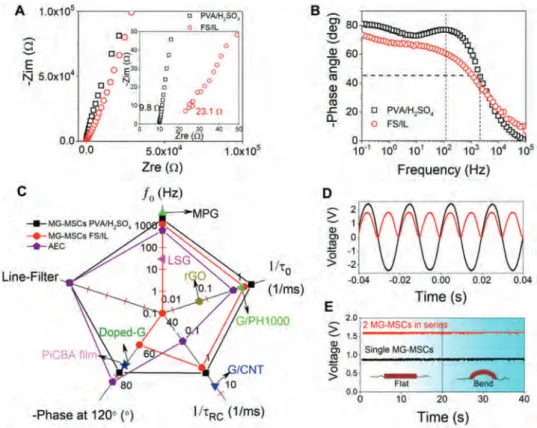
Electrochemical impedance spectroscopy (EIS) has been used to further investigate the frequency response of MG-MSCs on PET/Au in PVA/H2SO4 hydrogel and FS/IL ionogel
electrolytes. The Nyquist plots shown in Figure 3A are typical from capacitive, blocking electrodes and an equiva-lent series resistance of 9.8 Ω in PVA/H2SO4 electrolyte or
23.1 Ω in FS/IL electrolyte is obtained. From the curves of phase angle versus frequency (Figure 3B), the characteristic frequency f0 at −45° is 2025 Hz (in PVA/H2SO4) and 1150 Hz
(in FS/IL), corresponding to a time constant (τ0) of 0.49 and
0.87 ms, for PVA/H2SO4 and FS/IL electrolyte, respectively.
These values are lower than or comparable to those reported from ultrathin graphene-based MSCs in hydrogel electro-lyte (Figure 3C), e.g., UPSCs-25 (G/PH000, 1 ms),[14]
MPG-MSCs (0.28 ms),[19] SG-MSCs (0.26 ms),[30] azulene-bridged
coordination polymer framework film (coordination of 2,2′-diisocyano-1,1′,3,3′-tetraethoxycarbonyl-6,6′-biazulene (donted as iCBA), PiCBA, 0.27 ms),[31] G/CNTCs-MCs
(0.82 ms),[33] and PRG-MSCs (16.4 ms) (Table S1, Supporting
Figure 3. High-frequency response of flexible AC-line filtering devices. A) Nyquist plots of MG-MSCs in PVA/H2SO4 gel electrolyte (black) and FS/IL
ionogel electrolyte (red). Inset shows the magnified plots in the high-frequency region. B) Impedance phase angle versus frequency. C) Radar plot of MG-MSCs, compared with Al electrolytic capacitor (AEC) and carbon-based MSCs. D) AC input signal and rectified pulsating DC signal. E) DC output of MG-MSCs. The inset shows that bending the device does not affect the charge storage.
Information),[16] indicating the efficient ion transport/electron
conductance in MG microelectrodes. The phase angle at 120 Hz was measured to be −76.2° with a RC time constant (τRC)
calculated from the imaginary capacitance of 0.54 ms in PVA/ H2SO4 (Figure S14, Supporting Information), one order lower
than Al electrolytic capacitor (AEC) (−83.4°, 8.3 ms),[40]
demon-strating the potential of MG-MSCs for flexible AC line-filtering device.[41] Scheme S1 (Supporting Information) shows an AC
line filtering electrical circuit composed of a full wave bridge rectifier, smoothing MG-MSCs and a load resistor. The input AC signal is generated by function generator (Vpeak= ±2.3 V,
50 Hz) and the full-bridge rectifier converts the AC signal to a pulsating DC signal (Figure 3D), which is converted to a smooth DC output by the MG-MSCs eventually. As can be seen in Figure 3E, single MG-MSC converts the rectified pulsating signal to a smooth DC output of ≈0.88 V and two MG-MSCs in series convert the signal to a stable output of ≈1.6 V. It is noted that there was no obvious change in DC output when the measurement was conducted under a bending of ≈60° and the
output power can reach up to 11 mW (for two MG-MSCs in series with an area of ≈3 cm2).
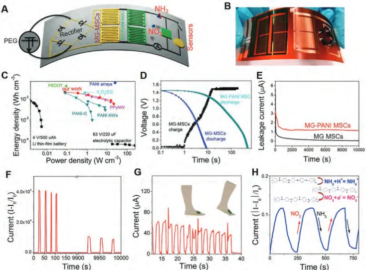
We demonstrate here that DLW is a universal protocol for the construction of an integrated energy harvesting device based on piezoelectric generator (PEG), MG-MSCs line-filtering, and gra-phene–polymer hybrid films/sensors (Figure 4A). We are also aware of the limitations of MG-MSCs in terms of areal capaci-tance or energy density (0.04 µWh cm−2) accompanying with the
very small thickness, which make MG-MSCs more suitable to be used in high power AC line-filtering devices. On the other hand, the capacitance was also optimized by depositing pseudocapaci-tive acpseudocapaci-tive materials on MG films. As shown in Scheme S2 (Sup-porting Information), MG films (4–8 layers) were used as con-ductive substrates for electrochemical deposition of PANI films with a size of 12 × 12 cm2 (Figure S15a, Supporting
Informa-tion). The SEM image (Figure S15b, Supporting Information) shows that the 245 nm thick PANI (from AFM image in the Figure S15c, Supporting Information) exhibits a uniform sur-face with a rod-like morphology on the top of MG film. Based
Figure 4. Design of flexible, integrated devices. A) Schematic and electrical circuit diagram of an integrated energy harvesting device made on PI.
B) Photograph of the integrated energy harvesting/pressure/gas sensors device. C) Ragone plots for MG-PANI MSCs with comparison to reported energy storage devices in PVA/H2SO4 electrolyte. D) Charging curve of the MG-MSCs by tapping the PEG and discharging curves of MG-MSCs and
MG-PANI MSCs at the current of 4 µA cm−2. E) Leakage currents of two MSCs over time. F–H) Response of current upon the detection of pressure
on the MG-PANI MSCs fabricated by DLW (Figure S15d, Sup-porting Information), the specific capacitance in PVA/H2SO4
electrolyte is improved to 3.8 mF cm−2 and 155 F cm−3 in device at 1 mV s−1 (Figure S16, Supporting Information). The obtained
MG-PANI MSCs demonstrate significantly improved energy densities of 21 mWh cm−3 (at 0.08 W cm−3) in PVA/H
2SO4
elec-trolyte and 34 mWh cm−3 (at 1.2 W cm−3) in poly(methyl meth-acrylate) (PMMA)/LiClO4 electrolyte (Figure 4C; Figure S17 and
Table S3, Supporting Information), comparable to or higher than those of state-of-the-art MSCs such as polypyrrole (PPy) nanowires, V2O5/exfoliated graphene MSCs using similar
elec-trode thickness.[42] The rod-like, intertwined PANI morphology
has also contributed to the ultraflexibility and exceptional mechanical stability of MG-PANI MSCs, as indicated by the high capacitance retention of 86% when the device is bent at an angle of 150° for 1000 cycles in PVA/H2SO4 electrolyte (Figures
S18 and S19, Supporting Information).
An integrated device, containing a diode bridge rectifier cir-cuit, two MG-MSC line-filter devices in series, MG-PANI MSCs array (2 × 2) (both in PVA/H2SO4 electrolyte), and pressure/gas
sensors is fabricated in one step by DLW on PI/Au substrate (Figure 4B). The input AC signal is generated by pressing PEG at a frequency of 110 Hz, which is smoothed by the MG-MSC line-filter and eventually stored by MG-PANI MSCs. After charging the MG-MSCs, the DC voltage smoothly reaches ≈1.5 V (Figure 4D). The charged MG-MSCs and MG-PANI MSCs can be galvanostatically discharged at 4 µA cm−2 for ≈9 s
and ≈500 s, respectively. From the current leakage evaluation of the devices (Figure 4E), we can see that the leakage current quickly drops to only 1.3 µA (0.4 µA cm−2) for MG-PANI MSCs
and 120 nA for MG-MSCs, respectively, indicating the high stability of the MSCs. The pressure detector shows a steady response to pressure pulses (≈5 kPa), as shown in Figure 4F. The on/off ratio remains 10 000 after 10 000 s. The sensor with integrated MG-PANI MSCs successfully detected walking. As shown in Figure 4G, repeated measurements of each step give regular signals, signifying the reproducible sensing powered by the integrated MSC array and potential applications in wearable energy storage. The response current gradually decreases with time, which is attributed to the gradual decrease in the output voltage of the charged MG-PANI MSCs with time. In addition, PANI gas sensors respond quickly to toxic gas such as 200 ppm of NO2 or NH3 with high sensitivity and fast response at room
temperature (22–25 °C) with the integrated device as power source;[43] the sensitivity tested also remains stable till 0 or
35 °C. As shown in Figure 4H, the different response to NO2 or
NH3 is explained by the transfer of electrons or protons between
PANI and gas molecules (inset of Figure 4H),[44] reflecting the
feasibility of the wearable, self-powered integrated device. In summary, we have demonstrated several prototypes of CVD-graphene-based in-plane MSCs with superior perfor-mances by DLW. The mass production and stable dry transfer of CVD graphene have guaranteed the highly stable interlayer distance of the multilayered graphene packing, benefiting to the efficient ion transport and simultaneously the excellent electric conductance of MG microelectrodes. The as-fabricated flexible MSCs delivered excellent specific volumetric power and energy densities and showed promising AC line-filtering performance with an extremely short RC time in PVA/H2SO4 electrolyte.
It should be noted that the areal capacitances or energy den-sities of MG-MSCs were limited by the very small thickness of MG electrodes restricted by the tedious sequential transfer process, though which can be carried out in an automatic way. The hybrid films made by depositing electrochemically active materials, such as conductive polymers on MG demonstrated above, have provided further opportunities for optimizing the performance of the MSC device. Some other strategies such as chemical doping or fine-tuning of structure/morphology may further increase the energy/power density of MG-based MSCs. The DLW fabrication process has shown potential for scaling to large area and for integration with other devices. We believe this study opens up a plethora of versatile design and scalable fabrication of flexible, on-chip devices for practically useful energy storage devices based on CVD graphene.
Experimental Section
Fabrication of MG-MSCs: The monolayer graphene films were obtained
by CVD on copper (Cu) substrates from Wuxi Graphene Film Co., Ltd. The layer-by-layer transfer of CVD graphene from Cu to target substrates was carried out with the assistance of PSA films, as previously reported with further modification.[25] Rollers (≈100 mm min−1) were used to assure the
adhesion between the graphene film grown on Cu with the adhesive layer. Before transfer, a 25 nm gold (Au) film was first sputtered on the substrate with a rate of ≈1.0 Å s−1 in a chamber with a pressure of ≈2 × 10⁻⁶ torr
(Kert Lesker Lab18) with a size of up to A4. After sequential transfers, MG films were obtained on various target substrates (e.g., PI, PTFE, PET, Si/ SiO2) coated with Au. For the fabrication of MG-MSCs, interdigital MG
microelectrodes were created by utilizing direct ultraviolet laser machining under ambient conditions (Design Comes True, DCT). The laser power and scanning speed were set as ≈1 W and 200 mm s−1, respectively. To
fabricate MG-MSCs, PVA/H2SO4 hydrogel electrolyte or FS/IL ionogel
electrolyte was slowly casted onto the surface of MG microelectrodes and solidified for overnight. The hydrogel electrolyte was prepared by mixing 6 g of PVA and 6 g of sulfuric acid (H2SO4) into 60 mL of deionized (DI)
water, and heated at 80 °C for 3 h under stirring. The ionogel electrolyte was prepared by mixing fumed silica nanopowder (particle size of 7–40 nm) with ionic liquid (EMI TFSI) with weight ratio of 0.01 g/1 g, and then the mixture was stirred for 10 h under an Ar atmosphere to produce a clear viscous ionogel (named as FS/IL).
Fabrication of MG-PANI MSCs: PANI was electrochemically deposited
on the MG films transferred on target substrates. For the deposition, the MG film was used as the working electrode in a three-electrode configuration that was constructed with a Pt plate as counter electrode and Ag/AgCl as reference electrode. The electrolyte was mixture of H2SO4 (0.5 m) and aniline (0.05 m) in H2O. The electropolymerization
of aniline on the MG film was performed at a constant potential of 0.75 V versus reference electrode for various durations. As-fabricated MG-PANI films were rinsed in DI water for several times and dried in a vacuum oven at room temperature. MG-PANI MSCs were fabricated by sequentially performing DLW of MG-PANI films and electrolyte casting following the same procedures as described above.
Characterizations and Electrochemical Evaluations: Material
characterizations were performed by SEM (JEOL-6700F, Japan), AFM (Veeco Nanoscope Icon, US), Raman (Renishaw, 532 nm laser, UK), XPS (Thermo ESCALAB 250, US) with Al Kα radiation (hv = 1486.6 eV), and contact angle measurement (Dataphysics, OCA20, Germany). The electrochemical properties were examined by CV, galvanostatic charge and discharge, and EIS recorded in the frequency range of 0.1 Hz–100 kHz with a 5 mV AC amplitude, on a PARSTAT MC electrochemical workstation (AMETEK, US). An AC line filtering circuit was composed of four diodes (1N4007), a resistor, and MG-MSCs made on PI substrate. The output signal was measured using an oscilloscope (Tektronix, TDS2012C).
Supporting Information
Supporting Information is available from the Wiley Online Library or from the author.
Acknowledgements
This work was supported by the China Government 1000 Plan Talent Program, Natural Science Foundation of China (grant nos. 51322204 and 51772282). The authors thank the support from USTC Center for Micro-and Nanoscale Research and Fabrication.
Conflict of Interest
The authors declare no conflict of interest.
Keywords
direct laser writing, graphene, line-filtering, micro-supercapacitors, power density
[1] a) F. Béguin, V. Presser, A. Balducci, E. Frackowiak, Adv. Mater.
2014, 26, 2219; b) Y. Huang, M. Zhu, Y. Huang, Z. Pei, H. Li,
Z. Wang, Q. Xue, C. Zhi, Adv. Mater. 2016, 28, 8344; c) H. Li, Y. Hou, F. Wang, M. R. Lohe, X. Zhuang, L. Niu, X. Feng, Adv.
Energy Mater. 2017, 7, 1601847.
[2] D. R. Rolison, J. W. Long, J. C. Lytle, A. E. Fischer, C. P. Rhodes, T. M. McEvoy, M. E. Bourg, A. M. Lubers, Chem. Soc. Rev. 2009, 38, 226.
[3] a) M. Beidaghi, Y. Gogotsi, Energy Environ. Sci. 2014, 7, 867; b) Y. Huang, M. Zhong, F. Shi, X. Liu, Z. Tang, Y. Wang, Y. Huang, H. Hou, X. Xie, C. Zhi, Angew. Chem., Int. Ed. 2017, 56, 9141. [4] M. F. El-Kady, R. B. Kaner, Nat. Commun. 2013, 4, 1475. [5] M. Xu, T. Liang, M. Shi, H. Chen, Chem. Rev. 2013, 113, 3766. [6] D. Pech, M. Brunet, H. Durou, P. Huang, V. Mochalin, Y. Gogotsi,
P.-L. Taberna, P. Simon, Nat. Nanotechnol. 2010, 5, 651.
[7] a) M. F. El-Kady, V. Strong, S. Dubin, R. B. Kaner, Science 2012, 335, 1326; b) Z. S. Wu, A. Winter, L. Chen, Y. Sun, A. Turchanin, X. Feng, K. Müllen, Adv. Mater. 2012, 24, 5130.
[8] S. Bae, H. Kim, Y. Lee, X. Xu, J.-S. Park, Y. Zheng, J. Balakrishnan, T. Lei, H. R. Kim, Y. I. Song, Nat. Nanotechnol. 2010, 5, 574. [9] Z. Liu, Z. S. Wu, S. Yang, R. Dong, X. Feng, K. Müllen, Adv. Mater.
2016, 28, 2217.
[10] Z. S. Wu, K. Parvez, A. Winter, H. Vieker, X. Liu, S. Han, A. Turchanin, X. Feng, K. Müllen, Adv. Mater. 2014, 26, 4552.
[11] Y. J. Lin, Y. Gao, Z. Y. Fan, Adv. Mater. 2017, 29, 1701736.
[12] a) X. Yang, C. Cheng, Y. Wang, L. Qiu, D. Li, Science 2013, 341, 534; b) Y. Zhu, S. Murali, M. D. Stoller, K. Ganesh, W. Cai, P. J. Ferreira, A. Pirkle, R. M. Wallace, K. A. Cychosz, M. Thommes, D. Su, E. A. Stach, R. S. Ruoff, Science 2011, 332, 1537.
[13] a) M. Xue, F. Li, J. Zhu, H. Song, M. Zhang, T. Cao, Adv. Funct.
Mater. 2012, 22, 1284; b) Z. S. Wu, G. Zhou, L. C. Yin, W. Ren, F. Li,
H. M. Cheng, Nano Energy 2012, 1, 107.
[14] Z. S. Wu, Z. Liu, K. Parvez, X. Feng, K. Müllen, Adv. Mater. 2015, 27, 3669.
[15] J. J. Yoo, K. Balakrishnan, J. Huang, V. Meunier, B. G. Sumpter, A. Srivastava, M. Conway, A. L. Mohana Reddy, J. Yu, R. Vajtai, Nano
Lett. 2011, 11, 1423.
[16] S. Wang, Z. S. Wu, S. Zheng, F. Zhou, C. Sun, H.-M. Cheng, X. Bao,
ACS Nano 2017, 11, 4283.
[17] D. Qi, Y. Liu, Z. Liu, L. Zhang, X. Chen, Adv. Mater. 2016, 29, 1602802.
[18] Z. Niu, L. Zhang, L. Liu, B. Zhu, H. Dong, X. Chen, Adv. Mater.
2013, 25, 4035.
[19] Z. S. Wu, K. Parvez, X. Feng, K. Müllen, Nat. Commun. 2013, 4, 2487. [20] P. Huang, C. Lethien, S. Pinaud, K. Brousse, R. Laloo, V. Turq,
M. Respaud, A. Demortiere, B. Daffos, P.-L. Taberna, B. Chaudret, Y. Gogotsi, P. Simon, Science 2016, 351, 691.
[21] J. Y. Hwang, M. Li, M. F. El-Kady, R. B. Kaner, Adv. Funct. Mater.
2017, 27, 1605745.
[22] a) J. Cai, C. Lv, A. Watanabe, Nano Energy 2016, 30, 790; b) Y. Y. Peng, B. Akuzum, N. Kurra, M. Q. Zhao, M. Alhabeb, B. Anasori, E. C. Kumbur, H. N. Alshareef, M.-D. Ger, Y. Gogotsi,
Energy Environ. Sci. 2016, 9, 2847.
[23] J. Lin, Z. Peng, Y. Liu, F. Ruiz-Zepeda, R. Ye, E. L. Samuel, M. J. Yacaman, B. I. Yakobson, J. M. Tour, Nat. Commun. 2014, 5, 5714.
[24] W. Gao, N. Singh, L. Song, Z. Liu, A. L. M. Reddy, L. Ci, R. Vajtai, Q. Zhang, B. Wei, P. M. Ajayan, Nat. Nanotechnol. 2011, 6, 496. [25] S. J. Kim, T. Choi, B. Lee, S. Lee, K. Choi, J. B. Park, J. M. Yoo,
Y. S. Choi, J. Ryu, P. Kim, Nano Lett. 2015, 15, 3236.
[26] H. Ji, X. Zhao, Z. Qiao, J. Jung, Y. Zhu, Y. Lu, L. L. Zhang, A. H. MacDonald, R. S. Ruoff, Nat. Commun. 2014, 5, 3317. [27] A. C. Ferrari, J. Meyer, V. Scardaci, C. Casiraghi, M. Lazzeri,
F. Mauri, S. Piscanec, D. Jiang, K. Novoselov, S. Roth, Phys. Rev.
Lett. 2006, 97, 187401.
[28] J. Kim, H. Park, J. B. Hannon, S. W. Bedell, K. Fogel, D. K. Sadana, C. Dimitrakopoulos, Science 2013, 342, 833.
[29] L. Gao, W. Ren, H. Xu, L. Jin, Z. Wang, T. Ma, L. P. Ma, Z. Zhang, Q. Fu, L.-M. Peng, Nat. Commun. 2012, 3, 699.
[30] Z. S. Wu, Y. Z. Tan, S. Zheng, S. Wang, K. Parvez, J. Qin, X. Shi, C. Sun, X. Bao, X. Feng, J. Am. Chem. Soc. 2017, 139, 4506. [31] C. Yang, K. S. Schellhammer, F. Ortmann, S. Sun, R. Dong,
M. Karakus, Z. Mics, M. Löffler, F. Zhang, X. Zhuang, E. Cánovas, G. Cuniberti, M. Bonn, X. Feng, Angew. Chem., Int. Ed. 2017, 129, 3978. [32] M. R. Lukatskaya, S. Kota, Z. Lin, M.-Q. Zhao, N. Shpigel,
M. D. Levi, J. Halim, P.-L. Taberna, M. W. Barsoum, P. Simon, Nat.
Energy 2017, 2, 17105.
[33] J. Lin, C. Zhang, Z. Yan, Y. Zhu, Z. Peng, R. H. Hauge, D. Natelson, J. M. Tour, Nano Lett. 2012, 13, 72.
[34] B. Xie, Y. Wang, W. Lai, W. Lin, Z. Lin, Z. Zhang, P. Zou, Y. Xu, S. Zhou, C. Yang, F. Kang, C.-P. Wong, Nano Energy 2016, 26, 276. [35] J. G. Speight, Lange’s Handbook of Chemistry, Vol. 1, McGraw-Hill,
New York 2005.
[36] W.-Y. Tsai, P.-L. Taberna, P. Simon, J. Am. Chem. Soc. 2014, 136, 8722.
[37] J. Huang, B. G. Sumpter, V. Meunier, Chem. - Eur. J. 2008, 14, 6614. [38] J. P. Randin, E. Yeager, J. Electrochem. Soc. 1971, 118, 711.
[39] R. Mysyk, E. Raymundo-Pinero, F. Béguin, Electrochem. Commun.
2009, 11, 554.
[40] J. R. Miller, R. Outlaw, B. Holloway, Science 2010, 329, 1637. [41] Y. Rangom, X. Tang, L. F. Nazar, ACS Nano 2015, 9, 7248. [42] a) M. Zhu, Y. Huang, Y. Huang, H. Li, Z. Wang, Z. Pei, Q. Xue,
H. Geng, C. Zhi, Adv. Mater. 2017, 29, 1605137; b) P. Zhang, F. Zhu, F. Wang, J. Wang, R. Dong, X. Zhuang, O. G. Schmidt, X. Feng, Adv.
Mater. 2017, 29, 1604491.
[43] X. Yan, Z. Han, Y. Yang, B. Tay, Sens. Actuators, B 2007, 123, 107. [44] D. Bandgar, S. Navale, S. Nalage, R. Mane, F. Stadler, D. Aswal,