HAL Id: hal-02999716
https://hal.archives-ouvertes.fr/hal-02999716
Submitted on 2 Dec 2020
HAL is a multi-disciplinary open access
archive for the deposit and dissemination of
sci-entific research documents, whether they are
pub-lished or not. The documents may come from
teaching and research institutions in France or
abroad, or from public or private research centers.
L’archive ouverte pluridisciplinaire HAL, est
destinée au dépôt et à la diffusion de documents
scientifiques de niveau recherche, publiés ou non,
émanant des établissements d’enseignement et de
recherche français ou étrangers, des laboratoires
publics ou privés.
Novel Multirate Modulator for High Bandwidth
Multicell Converters
Thierry Meynard, Tiago Sa Ferreira, Guilherme Monteiro Rezende, Lenin
Martins Ferreira Morais, Victor Flores Mendes, Didier Flumian, Jérémi
Regnier
To cite this version:
Thierry Meynard, Tiago Sa Ferreira, Guilherme Monteiro Rezende, Lenin Martins Ferreira Morais,
Victor Flores Mendes, et al.. Novel Multirate Modulator for High Bandwidth Multicell Converters.
IEEE Transactions on Power Electronics, Institute of Electrical and Electronics Engineers, 2020,
pp.1-1. �10.1109/TPEL.2020.3032118�. �hal-02999716�
Novel Multirate Modulator for High Bandwidth
Multicell Converters
Tiago S. Ferreira, Member, IEEE, Guilherme M. Rezende, Lenin M. F. Morais, Member, IEEE, Victor F. Mendes,
Didier Flumian, Jérémi Regnier, Member, IEEE and Thierry A. Meynard, Fellow, IEEE
Abstract- Series and parallel multicell converters have been introduced because they provide benefits in term of efficiency and power density. However, they also allow reducing the amount of energy stored in the filters, which potentially allows for faster dynamic responses. Interleaving the control patterns of different cells is another distinctive feature of these converters and is also the root of another potential improvement of the dynamic response: with one PWM update at each subcycle of the switching period, a n-cell converter may change its average output voltage over each of these intervals, while standard converters can only control the voltage over half the switching period. In this paper, a general multirate modulation strategy taking advantage of this property, while avoiding overswitching, and compatible with any n-cell converter is proposed and validated by simulation and experimental results.
I. INTRODUCTION
n recent years, several topologies of converters have been reported in the literature to improve their performances, especially efficiency and power density. Among them, there are multilevel converters with some characteristic features [1], [2]:
1) they include several commutation cells, which are the building blocks of the converters;
2) the two-level chopped voltage and/or current waveforms of the different cells are added in the circuit to form voltage and/or current waveforms with more levels;
3) the control pattern can be interleaved to optimize the output total waveform;
4) the filters take advantage of these improved waveforms; storing less energy, they can be smaller than those of classical two-level converters.
Such multilevel converters are employed in a myriad of applications such as HVDC transmission and distribution, energy storage systems and electric vehicles as well as in the naval and aerospace industries [1], [3]–[7]. This wide range of end-uses imply in different requirements for each deployment of the technology. Thus, numerous converter configurations exist [8]–[13], as the well-known neutral point clamped (NPC) [14], the flying capacitor (FC) [15] and the cascaded H-bridge [16] topologies and others as the clamp-double [17] and double-zero [18] converters, each with its particularities.
Furthermore, many applications of multilevel converters may demand or benefit from a faster transient response and a broader stability margin [19]. There are many techniques to achieve fast transient response depending on the application and converter topology. A fast control can be obtained, for example, with analog control without microcontrollers if the electronic circuits are designed to include all structures (converter and control system) [20], [21]. This is better suited for simpler topologies such as buck converters or low power applications [22].
In [23] it is shown that, for the same perceived switched frequency, a multilevel converter can be faster and more stable than its two-level counterpart due to a reduced output filter. Another way to reach better transient response in the control of power converters is to use non-linear techniques instead of the classical linear approach, such as: predictive control [24]–[26], geometric control [27], adaptive control [28], [29], etc. These techniques however come at the expense of increased computational burden, which is still a limitation especially for high frequency applications. Therefore, classical controls are still widely used since they are simple and easy to implement.
Other important aspect of control systems in multilevel converters is the use of distributed control. In applications with high number of switches, the distributed structure is usually adopted due to the impossibility to control all converters cells using a single processor. Thus, a multirate sampling approach is beneficial to implement all control strategies [30]–[32].
Another important subject related to dynamics in multilevel converters is the modulation technique, since decreasing the modulator delay is one way to enhance the control performance [32], [33]. Two classical carrier-based modulation techniques are the Symmetrically Sampled PWM (SS-PWM) and the Asymmetrically Sampled PWM (AS-PWM). These are based in sampling the control quantities and updating the duty cycle of each individual cell in specific moments of the carrier wave. This is done once per cycle for the SS-PWM and twice per cycle for the AS-PWM. However, this sampling and updating limitation deteriorates modulator performance [32]–[34].
To prevent this, the Naturally Sampled PWM (NS-PWM) can be used [35]. This modulator updates the duty cycles of all cells at the same time whenever sampling occurs. Moreover, it is shown in [32] that this modulator is suitable for decentralized control structures, since using it allows the separation of switching, sampling and control frequencies, minimizing control and sampling time and allowing for an overall better control performance in low frequency multilevel converters.
Nevertheless, overswitching (multiple switching pulses per carrier cycle) may incur while using the NS-PWM since each cell can change its duty cycle at any moment. These extra pulses must be avoided since they generate extra losses and EMI problems. Although there are ways to eliminate this via hardware, the Multirate Symmetrically Sampled and Multirate Asymmetrically Sampled modulators (which will be referred to as MSS-PWM and MAS-PWM, respectively) proposed in this paper present a software implemented solution that select which cell can change its state without provoking overswitching. This novel multirate modulator is not dependent of the control strategy nor the multicell converter configuration, i.e., it is generalized for any number of cells in series and/or in parallel.
This paper will focus on multicell series and parallel converters for three reasons:
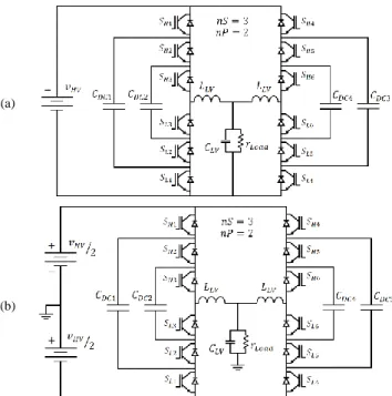
1) they can be used to build DC/DC or DC/AC (as depicted in Fig. 1(a) and Fig. 1(b) and, respectively) converters with any number of cells;
2) they can be combined to form series-parallel converters (in Fig. 1(a), 𝑆𝐻𝑖 and 𝑆𝐿𝑖 form cell 𝐼, with 𝑖 = 1, ⋯ ,6; cells 1 to 3
form a series three-cell inverter leg and cells 1 to 6 form a 3x2 series-parallel multicell inverter leg);
3) they are convenient to illustrate how some principles are common to series and parallel types and also to point out some differences.
The aim of this paper is to better understand the dynamic performance of series and parallel multicell converters by identifying their physical limits, showing how they can be maximized and comparing results obtained with different numbers of cells. In order to ensure fair comparison between the converters, three rules discussed along the text are followed:
1) no overswitching is allowed (a switching cell must never undergo more than one ON-OFF in a switching period);
2) the output filters of converters with different numbers of cells are designed according to the same criteria, since the filter values obviously affect dynamic performances;
3) the control is adjusted in such way that the fastest response is reached without control saturation.
(a)
(b)
Fig. 1 a) DC/DC series-parallel multicell converter (2 parallel, 3 series) and (b) DC/AC series-parallel multicell converter (2 parallel, 3 series).
The two main contributions of this paper are:
1)
firstly and mainly, the introduction of a multirate modulation strategy that allows fast duty cycles changes while avoiding overswitching via software and that is more resilient to filter parameter deviation;2)
secondly, a better understanding of the influence of the number and configuration of cells in thefilter design and control dynamic behavior.The superior performance of the proposed multirate method is demonstrated in simulations using the PLECS platform, and the impact of the number of cells on the system response is evaluated for parallel converters. The results are validated using an experimental prototype of a DC/DC three-cell converter.
The paper is organized as follows: Section II describes the filter design principles for series and parallel converters, Section III draws the physical performance limit of such converters, Section IV presents the control strategy employed, Section V describe the classical modulation and the proposed method, Section VI shows the simulation and experimental results, and finally in Section VII the conclusions are presented.
II. FILTER DESIGN FOR MULTICELL CONVERTERS
Filter design is not an easy task and it is not the main aim of this paper, so the development carried out here will be kept as simple as possible. Still, it is necessary to identify simple design rules and always apply them in such way that direct comparison can be done to identify the inherent differences of using different numbers of cells in series and/or in parallel.
Firstly, equations that govern the inductor current ripple and the capacitor voltage ripple in DC-DC converter structures as the one in Fig. 1(a) are derived, then it is discussed how these ripples influences the design of the filter. Finally, it is shown how the filter obeying chosen rules evolves with the number of cells in series and in parallel.
A. Inductor Current Ripple
The voltage delivered at the output of a series (𝑠) multicell converter with 𝑛𝑠 cells in series and interleaved control (control
patterns of the different cells identical but phase-shifted by 2𝜋/𝑛𝑠) is a square voltage waveform with an amplitude 𝑉𝐻𝑉/𝑛𝑠 and an
apparent frequency 𝑛𝑠∙ 𝑓𝑆𝑤 (where 𝑓𝑆𝑤 is the switching frequency). In consequence, the inductor current ripple is given by [36]
∆𝐼𝑝𝑘𝑝𝑘= 𝑉𝐻𝑉/(4 ∙ 𝐿𝑓∙ 𝑓𝑆𝑤∙ 𝑛𝑠2), (1)
where ∆𝐼𝑝𝑘𝑝𝑘 is the current ripple peak-to-peak value, 𝑉𝐻𝑉 is the voltage in the high voltage side of the converter (input) and 𝐿𝑓 is
the equivalent filter inductor (low voltage side).
In a parallel (𝑝) multicell converter with 𝑛𝑝 cells in parallel, each inductor sees only a fraction of the current, but the voltage
applied is the same as for a two-level converter. To maintain the normalized ripple in each 𝐿𝐿𝑉 inductor (∆𝐼𝑝𝑘𝑝𝑘𝑐𝑒𝑙𝑙_𝑁), it is needed
∆𝐼𝑝𝑘𝑝𝑘𝑐𝑒𝑙𝑙_𝑁(𝐼𝐿𝑉/𝑛𝑝) = 𝑉𝐻𝑉/(4 ∙ 𝐿𝐿𝑉∙ 𝑓𝑆𝑤), (2)
where 𝐿𝐿𝑉 is the cell filter inductor. Using an interleaved modulation, the current ripple will be partially compensated [37], resulting
in a ripple of the total current divided by np
∆𝐼𝑝𝑘𝑝𝑘𝑡𝑜𝑡𝑎𝑙= ∆𝐼𝑝𝑘𝑝𝑘 𝑐𝑒𝑙𝑙_𝑁
(𝐼𝐿𝑉/𝑛𝑝)/𝑛𝑝
= 𝑉𝐻𝑉/(4 ∙ 𝐿𝐿𝑉∙ 𝑓𝑆𝑤)/𝑛𝑝,
(3) which can be rewritten as
∆𝐼𝑝𝑘𝑝𝑘𝑡𝑜𝑡𝑎𝑙= 𝑉𝐻𝑉/[4 ∙ (𝐿𝐿𝑉/𝑛𝑝) ∙ 𝑓𝑆𝑤∙ 𝑛𝑝2], (4)
where 𝐿𝐿𝑉/𝑛𝑝 is the inductance equivalent to the cell inductances in parallel. Comparing Eq. 1 and Eq. 4, it is seen that the total
current ripple of the series and parallel multicell converters can be described with a unified equation involving the equivalent output inductance and the total number of cells, no matter if they are in series, parallel or even in series-parallel
∆𝐼𝑝𝑘𝑝𝑘𝑡𝑜𝑡𝑎𝑙= 𝑉𝐻𝑉/(4 ∙ 𝐿𝑓∙ 𝑓𝑆𝑤∙ 𝑛𝑐𝑒𝑙𝑙2 ), (5)
𝐿𝑓 = 𝐿𝐿𝑉/𝑛𝑝, (6)
𝑛𝑐𝑒𝑙𝑙 = 𝑛𝑠∙ 𝑛𝑝. (7)
B. Capacitor Voltage Ripple
The inductor ripple current is assumed to flow into the capacitor and it provokes the voltage ripple. Keeping in mind that the frequency of the current ripple in the series, the parallel and the series-parallel multicell converter is always 𝑛𝑐𝑒𝑙𝑙. 𝑓𝑆𝑤 when the
control signals are appropriately interleaved, for all three cases the voltage ripple is [36] ∆𝑉𝑝𝑘𝑝𝑘= ∆𝐼𝑝𝑘𝑝𝑘𝑡𝑜𝑡𝑎𝑙 / (8 ∙ 𝐶𝐿𝑉∙ 𝑛𝑐𝑒𝑙𝑙∙ 𝑓𝑆𝑤), (8)
where 𝐶𝐿𝑉 is the filter capacitor.
C. Filter Design
The inductor of a 2nd order low voltage side filter is generally bigger and more expensive than the capacitor and it also generates
more losses. All these reasons push the designer to try to minimize the inductor size and this process may result of various complicated tradeoffs. However, as a first approach, it can be considered that 𝐿 ∙ 𝐼𝑝𝑘∙ 𝐼𝑟𝑚𝑠 is an acceptable indication of the size of
the inductor [38], [39]. Very high inductance values result in almost no ripple, but also very big inductors (high energy, 𝐿 ∙ 𝐼𝑑𝑐2 ).
However, very low inductance values would also result in very big inductors, because of high peak and RMS currents. This means that, in practice, the filter inductors are neither chosen based on filtering criteria nor on dynamic performances; their value is chosen to try to minimize their weight, cost and/or losses. A first rule of thumb is to choose the maximum normalized current ripple ∆𝐼𝑝𝑘𝑝𝑘𝑁
and, for the case of a series-parallel converter, through Eq. 5 yields 𝐿𝐿𝑉= 𝑉𝐻𝑉/(4 ∙ ∆𝐼𝑝𝑘𝑝𝑘𝑁 ∙ 𝐼𝐿𝑉/𝑛𝑝∙ 𝑓𝑆𝑤)/𝑛𝑠2, (9)
𝐶𝐿𝑉= (
𝐼𝐿𝑉
𝑉𝐻𝑉
) ∙ (∆𝐼𝑝𝑘𝑝𝑘𝑁 /∆𝑉𝑝𝑘𝑝𝑘𝑁 )/(8 ∙ 𝑓𝑆𝑤∙ 𝑛𝑠∙ 𝑛𝑝3), (10)
where ∆𝑉𝑝𝑘𝑝𝑘𝑁 is the normalized voltage ripple. In this work, these equations are used to design the filters and impose current and
voltage ripples of ∆𝐼𝑝𝑘𝑝𝑘𝑁 = 30% and ∆𝑉𝑝𝑘𝑝𝑘𝑁 = 0.5%.
Notably, the constraint in the parallel converter is the current ripple in each leg (cell). Designing the maximum ripple in the cell, the output current ripple will be smaller, and the capacitor will be designed for this ripple. For the series converter, the constraint is directly the output current ripple thus the capacitor will be bigger to keep the maximum voltage ripple.
D. Filter Calculation with the Number of Cells
By these rules, filters for multicell converters are easily designed, and the similarities/differences of series/parallel converters can be better understood. Table I gives the 2nd order filter characteristic values for both topologies using the value of ripple previously
mentioned, and considering a converter input voltage 𝑉𝐻𝑉= 100𝑉, maximum output current 𝐼𝐿𝑉= 20𝐴 and switching frequency
𝑓𝑆𝑤= 20kHz. These parameters are used throughout this work for simulation and experimental results.
III. DYNAMIC PERFORMANCES AND PHYSICAL LIMITS FOR MULTICELL CONVERTERS
The general trend is that increasing the number of cells allows increasing the cutoff frequency of the filter, so it must be possible to increase the dynamic performances. Before getting into more details about the control strategy that respects all the requirements of a feasible power converter with as fast as possible time response, a study of the physical limits of large-scale response time resulting of the fixed DC voltage is first developed. This limit is in fact relative and it will be used later to compare with the result of the proposed modulation strategy.
State plane analysis is a convenient tool to study the evolution of second order filters, and it will be first analyzed the simplest case, i.e., a step of the reference from 0% to 100% without any load. It is easy to understand that the voltage to be applied for fastest response is 100% for a first time interval 𝑇1, to deliver as much energy as possible to the filter, then 0% for second time interval 𝑇2,
to avoid voltage overshoot and allow current to reach zero at the time that the voltage reaches 100%; at this time the applied voltage must become 100% again to maintain the output voltage at the targeted value.
This process requires perfect timing, but in this specific undamped case, the trajectories are perfect circles and, since the angles in the state plane translate to fractions of the natural frequency, it can be seen from Fig. 2 that the minimal time response is 1/3 of the natural frequency. This principle can be generalized to a more realistic case, i.e., a loaded converter. The centers of the circles are now along a line with a slope imposed by the value of the load, and the trajectories are now logarithmic spirals that makes analytic calculation much more difficult (see Fig. 3).
It is however possible to find numerically the values of 𝑇1 and 𝑇2 corresponding to this case, using the following process:
TABLE I
FILTER PARAMETERS: 𝑉𝐻𝑉= 100V, 𝐼𝐿𝑉= 20A, 𝑓𝑆𝑤= 20kHz
(SERIES “𝑠” AND PARALLEL “𝑝” CONVERTER CONFIGURATIONS) 𝑛𝑐𝑒𝑙𝑙 1 2 3 4 5 6 7 𝐶𝐿𝑉 (µF) 𝑝 75 9.3 2.8 1.17 0.6 0.35 0.2 𝑠 75 37.5 25 18.75 15 12.5 10.7 𝐿𝐿𝑉 (µH) 𝑝 208 416 625 833 1041 1250 1458 𝑠 208 52 23.1 13 8.3 5.8 4.2
Fig. 3 Optimal response of loaded converter.
1) write the model equations as functions of applied voltage, filter parameters and load; 2) impose initial conditions of point 𝐴 and find first trajectory with full applied voltage;
3) impose final conditions of point 𝐵 and find second trajectory by reverse simulation with zero applied voltage (reverse means a negative step at each iteration);
4) find intersection of the two trajectories, times 𝑇1 and 𝑇2.
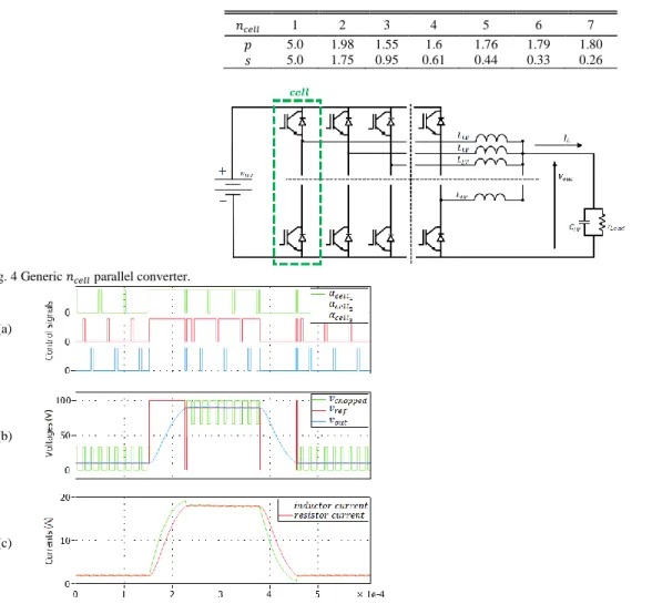
Using this method and considering the previously calculated filter parameters, Table II presents the optimal time responses as a function of the switching period (𝑡𝑠𝑊) of the loaded series and parallel converters for 𝑟𝐿𝑜𝑎𝑑 = 5 Ω (rated load resistance). It is seen
that the response varies with the number of cells and with the series and parallel structures.
The simulation results for a parallel converter as the one from Fig. 4 with 𝑛𝑐𝑒𝑙𝑙= 3 and 𝑟𝐿𝑜𝑎𝑑 = 5 Ω are shown in Fig. 5.
TABLE II
OPTIMAL TIME RESPONSE (MULTIPLES OF 𝑡𝑠𝑊): 𝑉𝐻𝑉= 100V,
𝐼𝐿𝑉= 20A, 𝑓𝑆𝑤= 20kHz AND RATED 𝑟𝐿𝑜𝑎𝑑= 5Ω
(SERIES “𝑠” AND PARALLEL “𝑝” CONVERTER CONFIGURATIONS) 𝑛𝑐𝑒𝑙𝑙 1 2 3 4 5 6 7
𝑝 5.0 1.98 1.55 1.6 1.76 1.79 1.80 𝑠 5.0 1.75 0.95 0.61 0.44 0.33 0.26
Fig. 4 Generic 𝑛𝑐𝑒𝑙𝑙 parallel converter.
(a)
(b)
(c)
output voltage and (c) cell current (inductor), output current (load).
From Fig. 5, the response time is 1.55 ∙ 𝑡𝑠𝑊 = 77.54µs for a voltage output step on the loaded converter, value that is in close
agreement with the one shown in Table II. Despite giving the “optimal response”, calculating 𝑇1 and 𝑇2 is not trivial and, thus, it is
hard to implement in a microprocessor for the control of multicell converters.
These trajectories and minimum response times are ideal optima that do not respect most limitations of practical setups (i. e. they represent theoretical physical limits). These will be used as comparison references, since they cannot be achieved by practical converters with sampling, delays, etc.
IV.CLOSED LOOP CONTROL OF OUTPUT VOLTAGE IN MULTICELL CONVERTERS
A. Inductor Current Ripple
As demonstrated previously, an appropriate filter design allows taking advantage of the multicell topologies to reduce the output filter size. In the same way, increasing the number of cells favor higher filter cutoff frequencies, implying that faster dynamics could be expected. In contrast, seeking high bandwidth for the output voltage requires a system modeling with focus on specific points related to the control performances, including the modulator.
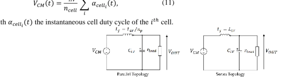
The equivalent filter model on Fig. 6 can be used for modeling the filter in series or parallel multicell converters. The output voltage 𝑉𝑂𝑈𝑇 depends on the filter parameters and on the common mode voltage 𝑉𝐶𝑀 provided by the converter. The filter includes
the equivalent inductor 𝐿𝑓 (and its equivalent winding resistance 𝑟𝐿𝑓), the capacitor 𝐶𝐿𝑉 and the load 𝑟𝐿𝑜𝑎𝑑.
Whatever the converter topology, 𝑉𝐶𝑀(𝑡) could be expressed as a composition of the single cell voltage contributions
𝑉𝐶𝑀(𝑡) = 𝑉𝐻𝑉 𝑛𝑐𝑒𝑙𝑙 ∑ 𝛼𝑐𝑒𝑙𝑙𝑖(𝑡) 𝑛𝑐𝑒𝑙𝑙 𝑖 , (11)
with 𝛼𝑐𝑒𝑙𝑙𝑖(𝑡) the instantaneous cell duty cycle of the 𝑖
𝑡ℎ cell.
Fig. 6 Filter equivalent circuit for parallel and series topologies.
To be suitable for the control design, Eq. 11 must be transformed into its mean value formulation. The mean value 𝑉𝐶𝑀 of the
converter voltage is written with Eq. 12 by introducing an equivalent mean common mode duty cycle 𝛼𝐶𝑀.
𝑉𝐶𝑀= 𝑉𝐻𝑉 𝑛𝑐𝑒𝑙𝑙 ∑ 𝛼𝑐𝑒𝑙𝑙𝑖(𝑡) 𝑛𝑐𝑒𝑙𝑙 𝑖 = 𝑉𝐻𝑉∙ 𝛼𝐶𝑀 (12)
Using the previous formulation, a generalized state space system of the converter-filter can be established:
[ 𝐼𝐿̇ 𝑉𝑂𝑈𝑇̇ ] = [ −𝑟𝐿𝑓 𝐿𝑓 − 1 𝐿𝑓 1 𝐶𝐿𝑉 1 𝑟𝑙𝑜𝑎𝑑𝐶𝐿𝑉] [𝑉𝐼𝐿 𝑂𝑈𝑇] + [ 𝑉𝐻𝑉 𝐿𝑓 0 ] 𝛼𝐶𝑀. (13)
B. Closed loop control of the output voltage
To be suitable for a closed loop control, the state space model in Eq. 13 must be discretized at the sampling time 𝑡𝑠𝑎𝑚𝑝𝑙𝑒 [40]. In
a classical approach, the closed loop operation can be performed using discrete state space feedback with an integral action as in Fig. 7. A pole placement design allows calculating the feedback gains by choosing the desired closed loop performances required to generate the duty cycle 𝛼𝐶𝑀𝑘 [41]
𝛼𝐶𝑀𝑘= −[𝐾𝐿 𝐾𝑓 ] [
𝐼𝐿𝑘
𝑉𝑂𝑈𝑇𝑘
] − 𝐾𝑖∫(𝑉𝑟𝑒𝑓𝑘− 𝑉𝑂𝑈𝑇𝑘), (14)
where 𝛼𝐶𝑀𝑘 is the mean duty cycle in the discretized 𝑘 instant and 𝐾𝐿, 𝐾𝑓, 𝐾𝑖 are the gains of the state space feedback control. The
poles’ frequencies are chosen according to the desired time of first peak during the system’s step response. This time value is chosen as the minimum peak time in a 10% to 90% voltage step without duty cycle saturation. The peak time is selected using an iterative simulation which changes this set of gains to achieve the best time response with these restrictions. For the same control restrictions, improving the modulator yields better gains and better overall performance. Thus, Section V details the proposed multirate
modulator and Section VI shows its superior performance when compared to the classical ones.
V.MODULATION IN HIGH BANDWIDTH CONTROL OF MULTICELL CONVERTERS
A. Classical Modulator
The final objective of the control strategy is to generate the appropriated cell duty cycles 𝛼𝑐𝑒𝑙𝑙𝑖(𝑡) from 𝛼𝐶𝑀𝑘. To generate these
duty cycles, a PWM strategy is commonly implemented.
In the classical SS-PWM and AS-PWM, the discrete duty cycle 𝛼𝐶𝑀𝑘 is compared to 𝑛𝑐𝑒𝑙𝑙 triangular carrier signals with a phase
shift of 2𝜋/𝑛𝑐𝑒𝑙𝑙 [42]. To get the mean value of the common current and to avoid overswitching, 𝛼𝐶𝑀𝑘 is updated on specific events
related to the minimum or/and maximum values of the carrier signals. The duty cycle is then sampled with a period of 𝑡𝑠𝑎𝑚𝑝𝑙𝑒 =
𝑡𝑠𝑊/𝑛𝑐𝑒𝑙𝑙/𝑠𝑟𝑎𝑡𝑒, with the sampling rate 𝑠𝑟𝑎𝑡𝑒= 1 for symmetrical and 𝑠𝑟𝑎𝑡𝑒 = 2 for asymmetrical samplings. An example is shown
on Fig. 8 for 𝑛𝑐𝑒𝑙𝑙= 3 and an update related to the minimum value of each carrier (SS-PWM).
When a change occurs on the duty cycle command 𝛼𝐶𝑀𝑘, each cell duty cycle 𝛼𝑐𝑒𝑙𝑙𝑖 is transformed through a sampling process
with a cascaded delay, as depicted in Fig. 8. The real resulting duty cycle 𝛼𝐶𝑀_𝐸𝑄𝑘 is then different from the required 𝛼𝐶𝑀𝑘 in the
middle of the period, and the real mean output voltage 𝑉𝐶𝑀 is not rigorously equal to 𝑉𝐻𝑉∙ 𝛼𝐶𝑀. This implies that the state space
model of Eq. 13 using 𝛼𝐶𝑀 is not strictly representative of the real behavior of the whole controlled system. The same observations
can be done if the duty cycle 𝛼𝐶𝑀𝑘 is updated both on minimum and on maximum of the carrier signal (AS-PWM).
This sampling process strongly penalizes the control performances. Often omitted for slow bandwidth control by assuming that the duty cycle sampling process is perfect (𝛼𝐶𝑀_𝐸𝑄𝑘 = 𝛼𝐶𝑀𝑘), it will be shown in the following that this behavior matters when high
bandwidth control is requested.
B. Proposed Multirate Modulator
To reduce the influence of the sampling process on the output voltage control, a novel strategy is proposed to improve the generation of the cell duty cycles. The goal of such approach is to allow changes in all cell’s duty cycles for each event on the carrier signals, not only for the event related to a specific cell. For this purpose, the mean voltage provided by the converter is studied over a subcycle period defined by 𝑡𝑠𝑎𝑚𝑝𝑙𝑒.
Table III defines the notations used in this paper.
Depending on the number of cells and the sampling rate, a time window with duration 𝑡𝑠𝑎𝑚𝑝𝑙𝑒 starting from the sampling event
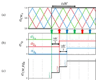
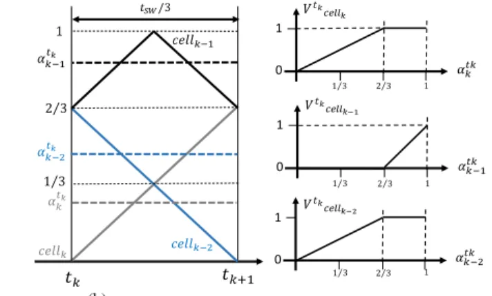
is used to extract the shape of the carrier signals. As an example, Fig. 9(a) depicts the shape of the carrier signals in a subcycle for a three-cell converter in which the duty cycle update occurs only when the carrier passes through a minimum. At each instant 𝑡𝑘,
regardless of which one is the active cell, the contribution of each cell to the global mean output voltage is defined for a three-cell converter as 𝑉𝑂𝑈𝑇𝑡𝑘 = (𝑉 𝑐𝑒𝑙𝑙𝑘 𝑡𝑘 + 𝑉𝑐𝑒𝑙𝑙 𝑘−1 𝑡𝑘 + 𝑉𝑐𝑒𝑙𝑙 𝑘−2 𝑡𝑘 ) 3⁄ . (15)
The comparison of the carrier signal with each duty cycle cell allows computing the mean voltage value of each of these cells over 𝑡𝑠𝑎𝑚𝑝𝑙𝑒. Hence, from Fig. 9(b), the mean voltage of each cell during one sample period is not a linear function of the cell duty
cycle as to a classical two-level converter.
This observation is a main point of the proposed approach. Usually neglected, this non-linearity constitutes a key point to improve the ability of the converter to provide a required voltage. With this, the objective is to find, at each 𝑡𝑘, the duty cycles
[𝛼𝑘𝑡𝑘, 𝛼
𝑘−1 𝑡𝑘 , 𝛼
𝑘−2
𝑡𝑘 ] to apply during the next period 𝑡
𝑠𝑎𝑚𝑝𝑙𝑒 to guarantee, if possible, the required output voltage 𝑉𝑂𝑈𝑇 𝑡𝑘 .
(a)
(b)
(c)
Fig. 8 Classical SS-PWM strategy for a three-cell converter: (a) shifted carriers signals and command, (b) cell duty cycle and (c) resultant duty cycle. TABLE III
DEFINITION OF USED VARIABLES 𝑐𝑒𝑙𝑙𝑘 : cell of which associated carrier signal equals 0 at 𝑡𝑘
𝑐𝑒𝑙𝑙𝑘−1 : cell of which associated carrier signal was equal to 0 at 𝑡𝑘−1
𝑐𝑒𝑙𝑙𝑘−2 : cell of which associated carrier signal was equal to 0 at 𝑡𝑘−2
𝑉𝑐𝑒𝑙𝑙𝑡𝑘𝑘
: average normalized voltage on [𝑡𝑘, 𝑡𝑘+1] generated by 𝑐𝑒𝑙𝑙𝑘
𝑉𝑐𝑒𝑙𝑙
𝑘−1
𝑡𝑘 : average normalized voltage on [𝑡
𝑘, 𝑡𝑘+1] generated by 𝑐𝑒𝑙𝑙𝑘−1
𝑉𝑐𝑒𝑙𝑙𝑘−2
𝑡𝑘 : average normalized voltage on [𝑡
𝑘, 𝑡𝑘+1] generated by 𝑐𝑒𝑙𝑙𝑘−2
𝛼𝑘𝑡𝑘 : signal sent to the non-inverting input of comparator 𝑘 during
[𝑡𝑘, 𝑡𝑘+1]
𝛼𝑘−1𝑡𝑘 : signal sent to the non-inverting input of comparator 𝑘 − 1
during [𝑡𝑘, 𝑡𝑘+1]
𝛼𝑘−2
𝑡𝑘 : signal sent to the non-inverting input of comparator 𝑘 − 2
during [𝑡𝑘, 𝑡𝑘+1]
While knowing that every cell can change its state twice (at any time, once for the positive carrier slope and once for the negative), the first task is to verify which cell has already switched during its own PWM cycle. With this, considering that the converter mean voltage output is given by Eq. 15, it is possible to calculate using Eq. 16 the required voltage (𝑉𝑜) to be synthesized by the cells that
are still able to switch. Since overswitching is not allowed, the state of the cells that already switched cannot be changed and their contributions (𝑉𝑘𝑠𝑤𝑖𝑡𝑐ℎ𝑒𝑑) to the desired converter output voltage 𝑉𝑂𝑈𝑇
𝑡𝑘
is already defined. 𝑉𝑂𝑈𝑇𝑡𝑘 = 1
𝑛𝑐𝑒𝑙𝑙
∙ (𝑉𝑜+ ∑ 𝑉𝑘𝑠𝑤𝑖𝑡𝑐ℎ𝑒𝑑) (16)
Thus, an additional “watchdog” must be included to avoid the overswitching. For this purpose, it is defined new variables 𝑒𝑛𝑘−1
and 𝑒𝑛𝑘−2 respecting the rules presented in Table IV. With these rules, four different cases can be distinguished:
1) Case 0: if [𝑒𝑛𝑘−1, 𝑒𝑛𝑘−2] = [0,0], 𝑐𝑒𝑙𝑙𝑘−1 and 𝑐𝑒𝑙𝑙𝑘−2 already switched. Only 𝛼𝑘𝑡𝑘 is free to be chosen as
𝛼𝑘𝑡𝑘= 2 ∙ 𝑉𝑡𝑘𝑂𝑈𝑇−
2 3(𝑉
𝑡𝑘
𝑐𝑒𝑙𝑙𝑘−1+ 𝑉𝑡𝑘𝑐𝑒𝑙𝑙𝑘−2). (17)
2) Case 1: if [𝑒𝑛𝑘−1, 𝑒𝑛𝑘−2] = [0,1], 𝑐𝑒𝑙𝑙𝑘−1 already switched. 𝛼𝑘𝑡𝑘 and 𝛼𝑘−2𝑡𝑘 are free to be chosen as
𝛼𝑘𝑡𝑘= 𝛼𝑘−2𝑡𝑘 = 𝑉𝑡𝑘𝑂𝑈𝑇−
1 3𝑉
𝑡𝑘−1
𝑐𝑒𝑙𝑙𝑘−1. (18)
3) Case 2: if [𝑒𝑛𝑘−1, 𝑒𝑛𝑘−2] = [1,0], 𝑐𝑒𝑙𝑙𝑘−2 already switched 𝛼𝑘𝑡𝑘 and 𝛼𝑘−1𝑡𝑘 are free to be chosen as
𝛼𝑘𝑡𝑘= 𝛼𝑘−1𝑡𝑘 = 2 ∙ 𝑉𝑡𝑘𝑂𝑈𝑇− 2 3𝑉 𝑡𝑘−1 𝑐𝑒𝑙𝑙𝑘−2, (19) for 𝑉𝑡𝑘 𝑐𝑒𝑙𝑙𝑘+ 𝑉𝑡𝑘𝑐𝑒𝑙𝑙𝑘−1< 1, and 𝛼𝑘𝑡𝑘= 𝛼𝑘−1𝑡𝑘 = 𝑉𝑡𝑘𝑂𝑈𝑇− 1 3𝑉 𝑡𝑘−1 𝑐𝑒𝑙𝑙𝑘−2+ 1 3, (20)
for 𝑉𝑡𝑘 𝑐𝑒𝑙𝑙𝑘+ 𝑉
𝑡𝑘
𝑐𝑒𝑙𝑙𝑘−1> 1.
4) Case 3: if [𝑒𝑛𝑘−1, 𝑒𝑛𝑘−2] = [1,1], 𝛼𝑘𝑡𝑘 , 𝛼𝑘−1𝑡𝑘 and 𝛼𝑘−2𝑡𝑘 are free to be chosen. An infinity of solutions is possible under
respect of Eq. 16. It can be chosen for example as 𝛼𝑘𝑡𝑘= 𝛼𝑘−1𝑡𝑘 = 𝛼𝑘−2𝑡𝑘 = 𝑉𝑡𝑘𝑂𝑈𝑇, (21)
where[𝛼1𝑡𝑘, 𝛼2𝑡𝑘, 𝛼3𝑡𝑘] can finally be defined by arranging the duty cycles [𝛼𝑘𝑡𝑘, 𝛼𝑘−1𝑡𝑘 , 𝛼𝑘−2𝑡𝑘 ] by choosing the index 𝑘 equal to
the cell from which the carrier signal event comes from (1, 2 or 3). This is summarized in
Table V, where “𝑝𝑜𝑠” corresponds to the cell number related to the considered carrier signal event.
For the sake of simplicity and easier understanding, the proposed approach is detailed for a three-cell parallel converter and symmetrical sampling. It must be underlined that one advantage of the proposed strategy is to be extendable to whatever the number of cells and the sampling rate by building a generic algorithm parametrized by 𝑛𝑐𝑒𝑙𝑙 and the sampling rate 𝑠𝑟𝑎𝑡𝑒. Furthermore, since
the output voltage expression is the same for parallel and series topologies, such proposed multirate strategy is suitable for any of these converter topologies. From a practical point of view, the proposed strategy is implemented in C-language to be suitable for real-time running.
(a) (b)
Fig. 9 Hypothetical three-cell converter: (a) PWM carriers during one subcycle sampling period and (b) possible voltage contributions of each cell. TABLE IV
RULES FOR 𝑒𝑛𝑘−1 AND 𝑒𝑛𝑘−2 TO AVOID OVER-SWITCHING
𝑒𝑛𝑘−1
If 𝛼𝑘−1
𝑡𝑘−1 < 2/3, the cell 𝑐𝑒𝑙𝑙
𝑘−1 has already switched during the
last increasing phase of the carrier signal: 𝑒𝑛𝑘−1= 0 (no change
allowed on the duty cycle). If 𝛼𝑘−1𝑡𝑘−1 > 2/3, the cell 𝑐𝑒𝑙𝑙
𝑘−1 has not switched during the last
increasing phase of the carrier signal: 𝑒𝑛𝑘−1= 1 (change
allowed on the duty cycle).
𝑒𝑛𝑘−2
If 𝛼𝑘−2
𝑡𝑘−1 < 2/3, the cell 𝑐𝑒𝑙𝑙
𝑘−2 has not switched during the last
decreasing phase of the carrier signal: 𝑒𝑛𝑘−2= 1 (change
allowed on the duty cycle). If 𝛼𝑘−2
𝑡𝑘−1 > 2/3, the cell 𝑐𝑒𝑙𝑙
𝑘−2 has already switched during the
last decreasing phase of the carrier signal: 𝑒𝑛𝑘−2= 0 (no
change allowed on the duty cycle). TABLE V
MULTIRATE ALGORITHM RULES TO AVOID OVER-SWITCHING Step 1 - Determination of [𝛼𝑘−1 𝑡𝑘−1, 𝛼 𝑘−2 𝑡𝑘−1] = 𝑓(𝑝𝑜𝑠, 𝛼 1 𝑡𝑘−1, 𝛼 3 𝑡𝑘−1, 𝛼 2 𝑡𝑘−1) Step 2 - Determination of [𝑒𝑛𝑘−1, 𝑒𝑛𝑘−2]= 𝑓(𝑝𝑜𝑠, 𝛼𝑘−1 𝑡𝑘−1 , 𝛼 𝑘−2 𝑡𝑘−1) Step 3 - Determination of [𝑉𝑐𝑒𝑙𝑙𝑡𝑘−1𝑘−1, 𝑉 𝑐𝑒𝑙𝑙𝑘−2 𝑡𝑘−1 ]=f (𝛼 𝑘−1 𝑡𝑘−1, 𝛼 𝑘−2 𝑡𝑘−1) Step 4 - Determination of [𝛼𝑘𝑡𝑘, 𝛼𝑘−1𝑡𝑘 , 𝛼𝑘−2𝑡𝑘 ]=f (𝑉𝑐𝑒𝑙𝑙𝑘−𝑖 𝑡𝑘−1 , 𝑉 𝑂𝑈𝑇 𝑡𝑘 , 𝑒𝑛 𝑘−1, 𝑒𝑛𝑘−2) Step 5 - Determination of [𝛼1𝑡𝑘, 𝛼2𝑡𝑘, 𝛼3𝑡𝑘]=f (𝛼𝑘𝑡𝑘, 𝛼𝑘−1𝑡𝑘 , 𝛼𝑘−2𝑡𝑘 , 𝑝𝑜𝑠 ) VI.RESULTS 𝑐𝑒𝑙𝑙𝑘 𝑐𝑒𝑙𝑙𝑘−2 𝑡𝑆𝑊/3 2 3⁄ 1 𝑐𝑒𝑙𝑙𝑘−1 𝑡𝑘 𝑡𝑘+1 𝛼𝑘−2𝑡𝑘 𝛼𝑘 𝑡𝑘 𝛼𝑘−1 𝑡𝑘 1 0 𝑉𝑡𝑘𝑐𝑒𝑙𝑙 𝑘 𝛼𝑘𝑡𝑘 1 3⁄ 1 0 𝑉𝑡𝑘𝑐𝑒𝑙𝑙 𝑘−1 𝛼𝑘−1𝑡𝑘 1 0 𝛼𝑘−2𝑡𝑘 2 3⁄ 1 2 3⁄ 1 1 3⁄ 2 3⁄ 1 1 3⁄ 𝑉𝑡𝑘𝑐𝑒𝑙𝑙 𝑘−2 1 3⁄
A. Considerations
The goal of this study is to determine the fastest response obtainable in closed loop operations using the classical SS-PWM and AS-PWM and comparing them with the proposed MSS-PWM and MAS-PWM. Only parallel converters will be assigned in the following. As already mentioned, the multirate modulator is directly transposable to series converters.
The definition of the “fastest response” implies taking into account the duty cycle saturation. In contrast to the classical small signal approach, the simulations are focused on a large-scale reference voltage step (from 10% to 90% of the DC bus voltage). In these conditions, the best reachable performance of a topology is defined as the fastest step response while respecting the duty cycles’ physical limits, i.e. 𝛼𝐶𝑀∈ [0,1].
The state space feedback gains are computed by choosing a specified time instant for the first peak value 𝑡𝑝𝑒𝑎𝑘 of the closed loop
output voltage with a damping ratio 𝜉 = 0.7 to ensure a corresponding voltage overshoot less than 5%. An iterative approach using numerical simulations is performed to find the fastest response according to the duty cycle limitations. Starting from a specified closed loop time response involving the duty cycle saturation (typically 𝑡𝑝𝑒𝑎𝑘 < 𝑡𝑜𝑝𝑡𝑖𝑚𝑎𝑙), 𝑡𝑝𝑒𝑎𝑘 is increased step by step until it is
find the first step response for which the duty cycle 𝛼𝐶𝑀 is less than one, meaning that the control does not saturate. This response
is then considered as the best for the situation under analysis and, thus, these control gains are used. Moreover, the following premises will be assumed in the simulations and for the experimental results: 1) 𝑉𝐻𝑉= 100𝑉 and 𝑓𝑆𝑤= 20kHz;
2) The filter is designed for each parallel converter, as the procedure described in Section II, i.e. the filter parameters of Table I are employed;
3) The controller gains are always calculated for each specific case in order to have the fastest possible response, changing with 𝑛𝑐𝑒𝑙𝑙, the filter parameters, the load and also with the modulation strategy.
B. Simulation Results – Parallel Multicell Converters
To illustrate the use of the previous algorithm, closed loop simulations are performed using parallel converters, as depicted in Fig. 4, for 𝑛𝑐𝑒𝑙𝑙∈ [1,7] with filter parameters of Table I and rated load resistance (𝑟𝐿𝑜𝑎𝑑= 5Ω). This allows comparing the
performances of the proposed multirate modulator with regard to the classical strategies of updating the cells duty cycles.
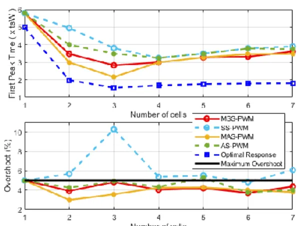
The step response performance changing the reference from 10% to 90% is evaluated using the first peak time 𝑡𝑝𝑒𝑎𝑘 expressed
as a function of the switching period 𝑡𝑠𝑤 and the overshoot for the different number of cells and different sampling rate, as depicted
in Fig. 10. In the same figure is also plotted the optimal time response of the output filter calculated as demonstrated in Section III and shown in Table II. This reference allows evaluating the distance between the control performances and the best obtainable physical responses.
The sampling process clearly reduces the bandwidth and the use of an asymmetrical sampling enhances the response for two and three cells. From Fig. 10, the time response with the proposed multirate modulation is improved in relation to the classical symmetrically and asymmetrically sampled ones no matter the number of cells, providing a closer-to-optimal response than the latter. As the classical approach does not accounts for the non-linearity of the system, the overshoot tends to be higher when compared to the proposed multirate.
Through Fig. 10, it is also observed that the fastest response can be achieved with a three-cell converter. This is a particular case for the chosen filter design that keeps the equivalent inductance (𝐿𝐿𝑉/𝑛𝑝) constant independently of the number of cells (see Table
I), while the capacitance drops with 𝑛𝑝3. The dynamics is more affected for smaller number of cells and tends to be constant
increasing the number of cells. The 𝑠𝑟𝑎𝑡𝑒 also has higher influence on converters with a smaller number of cells.
As the three-cell parallel converter has the fastest response in this case, it is the one chosen for study in the following sections.
Fig. 10 Closed loop system response of 𝑛𝑐𝑒𝑙𝑙 parallel converters using the SS-PWM, AS-PWM, MSS-PWM and MAS-PWM for rated resistance.
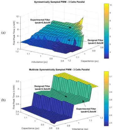
First, the effect of the variation of filter parameters on the three-cell parallel converter is investigated. The inductance and capacitance values presented in Table I are considered as a base and they are varied from −20% to +20%. Fig. 11(a) and (b) show the time of the first voltage peak as a function of 𝑡𝑠𝑊 for both classical SS-PWM and proposed MS-PWM, respectively.
It can be seen that, when the classical modulator is employed, the system is more prone to variations in the time response. In this case, the higher the inductance, the slower is the response. However, the most important factor is the capacitance: the higher it is the faster is the response.
When the multirate modulator is employed, the capacitance has almost no effect on the time response when evaluated individually, whereas the inductance has a small influence. One can notice that the multirate modulator reduces the effect of the parameters variation and always leads to a better response compared to the classical one.
Since the results from Fig. 11 consider a fixed load (rated current), Table VI shows the comparison of the time to reach the first voltage peak between both modulators for different load resistances. Furthermore, the optimal time is presented for sake of comparison. The system response is more affected when the classical modulator is employed and the proposed method has superior performance regardless of the load resistance.
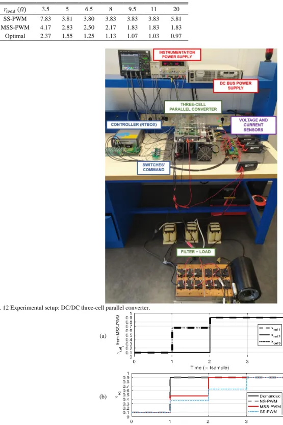
D. Experimental Setup – Three-Cell Parallel Converter
The experimental setup is constituted of a three-cell parallel converter. Its structure is the same as the one presented in Fig. 4 with 𝑛𝑐𝑒𝑙𝑙 = 3.
(a)
(b)
Fig. 11 Time response of three-cell parallel converter with closed loop control for 𝑟𝐿𝑜𝑎𝑑= 5 Ω: (a) SS-PWM and (b) proposed MSS-PWM.
Fuji Electric 2MBI300VB060 IGBT are used and the system is controlled by a PLECS RTBox with a deadtime of 1𝜇𝑠. Each individual carrier has a frequency of 𝑓𝑆𝑤= 20kHz, thus the sampling period is 𝑡𝑠𝑎𝑚𝑝𝑙𝑒′ = 16.6𝜇𝑠 for the symmetrically sampled
cases and 𝑡𝑠𝑎𝑚𝑝𝑙𝑒′′ = 8.3𝜇𝑠 for the asymmetrically sampled ones. The employed filter has similar parameters to the previous design.
In fact, there is a small difference in the prototype values (𝐿𝐿𝑉= 650µ𝐻, 𝐶𝐿𝑉= 2.5µ𝐹), that influences the system response mainly
in the SS-PWM, as demonstrated in the points signaled in Fig. 11. The workbench used on all tests is depicted in Fig. 12.
E. Experimental Results – Open Loop
First, an open loop study is made. For this, it is important to check the mean value of all individual 𝛼𝑐𝑒𝑙𝑙𝑖, which is the mean
equivalent duty cycle (𝛼𝑒𝑞) perceived by the converter. Fig. 13 shows 𝛼𝑒𝑞 for the classical SS-PWM, the proposed MSS-PWM and
also for the NS-PWM.
TABLE VI
𝑟𝑙𝑜𝑎𝑑 (𝛺) 3.5 5 6.5 8 9.5 11 20
SS-PWM 7.83 3.81 3.80 3.83 3.83 3.83 5.81 MSS-PWM 4.17 2.83 2.50 2.17 1.83 1.83 1.83 Optimal 2.37 1.55 1.25 1.13 1.07 1.03 0.97
Fig. 12 Experimental setup: DC/DC three-cell parallel converter.
(a)
(b)
Fig. 13 Experimental results in open loop and symmetrical sampling: (a) 𝛼𝑐𝑒𝑙𝑙 𝑖 with the MSS-PWM algorithm and (b) comparison between 𝛼𝑒𝑞 determined via the
NS-PWM, SS-PWM and MSS-PWM during a step in reference.
When updating duty cycles in multicell converters without overswitching, there is a time delay between calculated and synthetized equivalent duty cycles. This is due to the restriction that each cell can switch only in a certain proper time. As shown in Fig. 13, during the given step change, the multirate algorithm reaches the final desired reference level a whole sampling time earlier (twice as fast) than the classical SS-PWM approach, which reduces the aforementioned modulator delay.
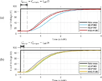
Fig. 14 shows the load voltage comparison of the NS-PWM, SS-PWM, AS-PWM, MSS-PWM and MAS-PWM for the rated load resistance (𝑟𝐿𝑜𝑎𝑑= 5 Ω) in open loop operation. The inherent time delays (𝑡𝑑𝑒𝑙𝑎𝑦) between computing the duty cycle and outputting
the commands are highlighted in the graph for each sampling strategy.
When the system is submitted to a change in the reference output voltage, the NS-PWM allows for a fast response by immediately updating the duty cycle of every single cell in the converter regardless of the occurrence of overswitching. Given that overswitching is a problem because it increases losses and causes EMI problems, it is desired that this behavior is avoided.
The classical SS-PWM and AS-PWM prevent the occurrence of overswitching by allowing the update of each cell duty cycle only once per carrier period. The proposed multirate PWM is a middle ground between the natural and classical PWMs: by determining which cell has already switched during its own PWM cycle and preventing their duty cycle from changing at a software (code) level, it allows the immediate update of all of the other cells’ duty cycles while avoiding overswitching. Thus, the proposed multirate is able to present faster responses than the classical SS-PWM and AS-PWM as observed from the curves presented in Fig. 14.
F. Experimental Results – Closed Loop
The load voltages from Fig. 14 present steady state error for all of the tested PWM methods. Therefore, even though the advantages of the proposed modulator can be seen in open loop, an enhancement of the response can be better in closed loop. Table VII shows the closed loop gains calculated for rated load resistance load for the tested modulation methods. Only the strategies without overswitching will be compared.
(a)
(b)
Fig. 14 Experimental results (time response) of the three-cell parallel converter in open loop with rated load: measured load voltages with (a) the SS-PWM, NS-PWM and MSS-NS-PWM and (b) the AS-NS-PWM, NS-NS-PWM and MAS-NS-PWM.
TABLE VII
DESIGNED CLOSED LOOP GAINS FOR EACH TESTED MODULATOR Modulator 𝐾𝐿 𝐾𝑓 𝐾𝑖
SS-PWM 0.0527 -0.0080 -123.4379 AS-PWM 0.1778 -0.0114 -619.7231 MSS-PWM 0.1049 -0.0039 -469.0183 MAS-PWM 0.2033 -0.0074 -924.3017
Trying to make the control extremely fast is a challenge in the prototype due to the inherent time delays between duty cycle computations and analog to digital conversions (ADC) of measurement samples. Using the measured quantities in the control leads to an unstable behavior since it has not been designed to compensate these delays. This particular point is out of the present paper scope.
To overcome this problem and validate the proposed method, a state space estimator [41] based on Eq. 13 is implemented to estimate the voltage and current used in the control instead of the measurements. In this configuration, it is possible to highlight the performances of the modulator regardless of the constraints related to the measurement delays. Nevertheless, it is important to highlight that the experimental results presented are from direct measurements of the output voltage.
The converter duty cycles are computed by the control, using the estimator and the modulator. The RT Box’s processor does this within the available calculation period of 16.6µ𝑠 for symmetrical sampling and 8.3µ𝑠 for asymmetrical sampling. To complete a computation cycle, it takes a total time of 1.1µ𝑠 for the multirate strategy (MSS-PWM and MAS-PWM) and 0.62µ𝑠 for the classical one (SS-PWM and AS-PWM). For the worst scenario of asymmetrical sampling, this means 13.3% and 7.5% of processor usage, respectively.
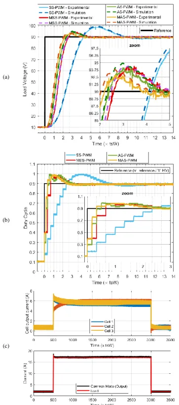
Fig. 15(a) shows the comparison of the SS-PWM, AS-PWM, MSS-PWM and MAS-PWM for rated load resistance (𝑟𝐿𝑜𝑎𝑑 = 5 Ω)
in closed loop operation. For the sake of validation, the simulation results are also plotted using the filter parameters of the experimental setup. In fact, the measurements have a delay of one sampling time in comparison with the simulation, because the digital control platform has an inherent calculation time and the command signal is only made available in its output in the next sampling period. For a more direct comparison, the simulation data is delayed by its modulator respective 𝑡𝑑𝑒𝑙𝑎𝑦 in the presented
graph.
(a)
(b)
(c)
Fig. 15 Experimental results (time response) of the three-cell parallel converter with closed loop control using the classical SS-PWM and AS-PWM and the proposed MSS-PWM and MAS-PWM: (a) load voltage, (b) duty cycle (control command) and (c) cells, common mode and load currents with MSS-PWM.
overshoot. This happens because the multirate modulator can effectively control the average value of the chopped voltage over each 𝑡𝑠𝑊/3 interval (instead of 𝑡𝑠𝑊 for the standard modulator). For the asymmetrical sampling cases, the response is faster with the
multirate modulator, but the improvement is marginal for this specific test. As already mentioned while discussing the simulation results and it will be reinforced by the experimental results, such improvement depends on the load and the filter.
It is also important to highlight that, in both cases, the control output (duty cycle) peaks at (but does not exceed) 100%, as in Fig. 15(b). This proves that both controllers were efficiently designed to maximize speed without distortion in this 10% to 90% voltage reference (𝑉𝑟𝑒𝑓𝑒𝑟𝑒𝑛𝑐𝑒) step. Thus, the enhancement in the system performance is due to the proposed method, not because of the
different control tuning for each load.
As shown in Fig. 15(c), the average current values of each cell converge to values that are very close to each other, with the differences between them being due to deviations inherent to the manufacturing process of the used inductors. This small unbalance in steady state exists for all the modulation strategies and it can be eliminated by using differential control techniques as the one presented in [43]. To disturb the common mode current as little as possible and have a fast response, the single constraint is to design the differential control with a low bandwidth with regard to the common mode dynamic.
Furthermore, it can be seen from Fig. 15(a) that the measured load voltage overshoot and first peak time for all tested modulators (specially for the multirate ones due to their resilience to parametric deviation) is in agreement with the information disclosed in Fig. 10 and Fig. 11 for 𝑛𝑐𝑒𝑙𝑙 = 3 and the previously discussed filter analysis is validated.
Fig. 16 shows results for the symmetrical and asymmetrical sampling strategies with different 𝑟𝐿𝑜𝑎𝑑. From it, the higher the
resistance (smaller current), the faster the response in all cases. The multirate modulator has faster responses than the classical strategy while keeping the overshoot within design constraints.
(a)
(b)
Fig. 16 Experimental results obtained by changing the load resistance (rated values): a) SS-PWM and MSS-PWM and b) AS-PWM and MAS-PWM.
G. Experimental Results – Steady State Analysis
To deepen the study of the proposed multirate modulator, it is fitting to carry out an analysis of its performance in steady state through zoom-ins on Fig. 14 and Fig. 15. Thus, Fig. 17 allow the comparison between the steady state load voltages’ waveforms with rated load for both the classical and multirate modulators. From all the curves shown in these figures, it is noted that the multirate modulator not only allows for faster responses with smaller overshoot, but it also does not provoke any degradation of the system’s performance in steady state.
VII.CONCLUSIONS
In this paper, a novel multirate modulator is proposed to improve the closed loop performances of the output voltage control of parallel and series converters. This modulator takes into account the non-linearity between the subcycle duty cycle and the subcycle average output voltage of multicell converters. A generic multirate modulator has been developed to be adaptable for any cell number and for the two different sampling strategies (symmetrical and asymmetrical). One of its advantages is that both the MSS-PWM and MAS-MSS-PWM are fully software implemented and overswitching is avoided.
(a)
(b)
Fig. 17 Experimental results of the three-cell parallel converter with rated load for both a 10𝑉 and a 90𝑉 voltage reference: steady state load voltages with the classical and multirate modulators in (a) open loop and (b) closed loop.
The reduction of the modulator delay will affect the overall control performance and it is one way to achieve a better global response. The open loop step responses demonstrate that the multirate modulator allow the converter’s mean equivalent duty cycle to reach steady state faster than the classical SS-PWM and AS-PWM. This improved performance also lead to better results for the closed loop tests. Thus, by using the multirate modulator, it is possible to obtain faster responses (without degrading the system’s steady state performance) and this can be a significant improvement when high bandwidth is required.
It was shown through simulations and experimental results that this proposed multirate strategy (the MSS-PWM and MAS-PWM) always surpasses the classical SS-PWM and AS-PWM regarding the reachable time response no matter the load and even considering a variation in the filter parameters. This concept is also immediately applicable to series converters since there is a duality between them.
Lastly, the effects of decreasing the modulator’s time might not be noticeable if the filter design is not proper. If this happens, the effects of the modulator’s delay reduction may be overshadowed by the slower dynamics imposed by the filter itself. In light of this, a study of the influence of the number and configuration of cells in the filter design and control dynamic behavior was presented. By optimizing the filter and having a quick multirate modulator, it is possible to design even faster controllers to have fast global responses.
REFERENCES
[1] J. Rodriguez et al., “Multilevel Converters: An Enabling Technology for High-Power Applications,” Proceedings of the IEEE, vol. 97, no. 11, pp. 1786– 1817, Nov. 2009, doi: 10.1109/JPROC.2009.2030235.
[2] R. Marquardt, “Modular Multilevel Converters: State of the Art and Future Progress,” IEEE Power Electron. Mag., vol. 5, no. 4, pp. 24–31, Dec. 2018, doi: 10.1109/MPEL.2018.2873496.
[3] H.-S. Kim, J.-W. Baek, M.-H. Ryu, J.-H. Kim, and J.-H. Jung, “The High-Efficiency Isolated AC–DC Converter Using the Three-Phase Interleaved LLC Resonant Converter Employing the Y-Connected Rectifier,” IEEE Transactions on Power Electronics, vol. 29, no. 8, pp. 4017–4028, Aug. 2014, doi: 10.1109/TPEL.2013.2290999.
[4] S. M. Goetz, Z. Li, X. Liang, C. Zhang, S. M. Lukic, and A. V. Peterchev, “Control of Modular Multilevel Converter With Parallel Connectivity— Application to Battery Systems,” IEEE Trans. Power Electron., vol. 32, no. 11, pp. 8381–8392, Nov. 2017, doi: 10.1109/TPEL.2016.2645884.
[5] D. Moon, J. Park, and S. Choi, “New Interleaved Current-Fed Resonant Converter With Significantly Reduced High Current Side Output Filter for EV and HEV Applications,” IEEE Transactions on Power Electronics, vol. 30, no. 8, pp. 4264–4271, Aug. 2015, doi: 10.1109/TPEL.2014.2360470.
[6] Y. Chen, S. Zhao, Z. Li, X. Wei, and Y. Kang, “Modeling and Control of the Isolated DC–DC Modular Multilevel Converter for Electric Ship Medium Voltage Direct Current Power System,” IEEE J. Emerg. Sel. Topics Power Electron., vol. 5, no. 1, pp. 124–139, Mar. 2017, doi: 10.1109/JESTPE.2016.2615071.
[7] H. Nademi, R. Burgos, and Z. Soghomonian, “Power Quality Characteristics of a Multilevel Current Source With Optimal Predictive Scheme From More-Electric-Aircraft Perspective,” IEEE Trans. Veh. Technol., vol. 67, no. 1, pp. 160–170, Jan. 2018, doi: 10.1109/TVT.2017.2779839.
[8] S. Kouro et al., “Recent Advances and Industrial Applications of Multilevel Converters,” IEEE Trans. Ind. Electron., vol. 57, no. 8, pp. 2553–2580, Aug. 2010, doi: 10.1109/TIE.2010.2049719.
[9] A. Dekka, B. Wu, R. L. Fuentes, M. Perez, and N. R. Zargari, “Evolution of Topologies, Modeling, Control Schemes, and Applications of Modular Multilevel Converters,” IEEE J. Emerg. Sel. Topics Power Electron., vol. 5, no. 4, pp. 1631–1656, Dec. 2017, doi: 10.1109/JESTPE.2017.2742938.
[10] K. K. Gupta, A. Ranjan, P. Bhatnagar, L. K. Sahu, and S. Jain, “Multilevel Inverter Topologies With Reduced Device Count: A Review,” IEEE Trans.
Power Electron., vol. 31, no. 1, pp. 135–151, Jan. 2016, doi: 10.1109/TPEL.2015.2405012.
[11] A. Prayag and S. Bodkhe, “A comparative analysis of classical three phase multilevel (five level) inverter topologies,” in 2016 IEEE 1st International
Conference on Power Electronics, Intelligent Control and Energy Systems (ICPEICES), Delhi, India, Jul. 2016, pp. 1–5, doi:
10.1109/ICPEICES.2016.7853567.
[12] A. I. Maswood and H. D. Tafti, Eds., Advanced multilevel converters and applications in grid integration. Hoboken, NJ: John Wiley & Sons, 2018. [13] F. Tardelli, A. Costabeber, D. Trainer, and J. Clare, “Series Chain-Link Modular Multilevel AC–DC Converter (SCC) for HVDC Applications,” IEEE
Transactions on Power Electronics, vol. 35, no. 6, pp. 5714–5728, Jun. 2020, doi: 10.1109/TPEL.2019.2952194.
[14] A. Nabae, I. Takahashi, and H. Akagi, “A New Neutral-Point-Clamped PWM Inverter,” IEEE Transactions on Industry Applications, vol. IA-17, no. 5, pp. 518–523, Sep. 1981, doi: 10.1109/TIA.1981.4503992.
[15] T. A. Meynard and H. Foch, “Multi-level conversion: high voltage choppers and voltage-source inverters,” in , 23rd Annual IEEE Power Electronics
Specialists Conference, 1992. PESC ’92 Record, Jun. 1992, pp. 397–403 vol.1, doi: 10.1109/PESC.1992.254717.
[16] F. Z. Peng, J.-S. Lai, J. W. McKeever, and J. VanCoevering, “A multilevel voltage-source inverter with separate DC sources for static VAr generation,”
IEEE Trans. on Ind. Applicat., vol. 32, no. 5, pp. 1130–1138, Oct. 1996, doi: 10.1109/28.536875.
[17] Y. Xue, Z. Xu, and G. Tang, “Self-Start Control With Grouping Sequentially Precharge for the C-MMC-Based HVDC System,” IEEE Trans. Power
Delivery, vol. 29, no. 1, pp. 187–198, Feb. 2014, doi: 10.1109/TPWRD.2013.2279106.
[18] C. Dahmen, F. Kapaun, and R. Marquardt, “Analytical investigation of efficiency and operating range of different Modular Multilevel Converters,” in 2017
IEEE 12th International Conference on Power Electronics and Drive Systems (PEDS), Honolulu, HI, Dec. 2017, pp. 336–342, doi:
10.1109/PEDS.2017.8289151.
[19] P. S. Niklaus, J. A. Anderson, D. Bortis, and J. W. Kolar, “Ultra-High Bandwidth GaN-Based Class-D Power Amplifier for Testing of Three-Phase Mains Interfaces of Renewable Energy Systems,” in 2019 8th International Conference on Renewable Energy Research and Applications (ICRERA), Brasov, Romania, Nov. 2019, pp. 615–622, doi: 10.1109/ICRERA47325.2019.8996585.
[20] Y.-C. Hsu, C.-Y. Ting, L.-S. Hsu, J.-Y. Lin, and C. C.-P. Chen, “A Transient Enhancement DC–DC Buck Converter With Dual Operating Modes Control Technique,” IEEE Trans. Circuits Syst. II, vol. 66, no. 8, pp. 1376–1380, Aug. 2019, doi: 10.1109/TCSII.2018.2883889.
[21] M. Zhou, Z. Sun, Q. W. Low, and L. Siek, “Multiloop Control for Fast Transient DC–DC Converter,” IEEE Trans. VLSI Syst., vol. 27, no. 1, pp. 219–228, Jan. 2019, doi: 10.1109/TVLSI.2018.2869430.
[22] H. Wu, T. Mu, H. Ge, and Y. Xing, “Full-Range Soft-Switching-Isolated Buck-Boost Converters With Integrated Interleaved Boost Converter and Phase-Shifted Control,” IEEE Transactions on Power Electronics, vol. 31, no. 2, pp. 987–999, Feb. 2016, doi: 10.1109/TPEL.2015.2425956.
[23] M. Katayama, T. Ohno, H. Obara, and A. Kawamura, “Application of Multi-Level Converter for Fast Current Control in Small-Scale DC Power Network,”
IEEE Trans. on Ind. Applicat., vol. 55, no. 3, pp. 2902–2909, May 2019, doi: 10.1109/TIA.2019.2896839.
[24] T. Dragicevic, “Model Predictive Control of Power Converters for Robust and Fast Operation of AC Microgrids,” IEEE Trans. Power Electron., vol. 33, no. 7, pp. 6304–6317, Jul. 2018, doi: 10.1109/TPEL.2017.2744986.
[25] B. S. Riar, T. Geyer, and U. K. Madawala, “Model Predictive Direct Current Control of Modular Multilevel Converters: Modeling, Analysis, and Experimental Evaluation,” IEEE Trans. Power Electron., vol. 30, no. 1, pp. 431–439, Jan. 2015, doi: 10.1109/TPEL.2014.2301438.
[26] F. Defay, A.-M. Llor, and M. Fadel, “A Predictive Control With Flying Capacitor Balancing of a Multicell Active Power Filter,” IEEE Trans. Ind. Electron., vol. 55, no. 9, pp. 3212–3220, Sep. 2008, doi: 10.1109/TIE.2008.927989.
[27] M. Mohammadi and M. Ordonez, “Fast Transient Response of Series Resonant Converters Using Average Geometric Control,” IEEE Trans. Power
Electron., vol. 31, no. 9, pp. 6738–6755, Sep. 2016, doi: 10.1109/TPEL.2015.2504489.
[28] L. V. Bellinaso, H. H. Figueira, M. F. Basquera, R. P. Vieira, H. A. Grundling, and L. Michels, “Cascade Control With Adaptive Voltage Controller Applied to Photovoltaic Boost Converters,” IEEE Trans. on Ind. Applicat., vol. 55, no. 2, pp. 1903–1912, Mar. 2019, doi: 10.1109/TIA.2018.2884904.
[29] S. Eren, M. Pahlevani, A. Bakhshai, and P. Jain, “An Adaptive Droop DC-Bus Voltage Controller for a Grid-Connected Voltage Source Inverter With LCL Filter,” IEEE Trans. Power Electron., vol. 30, no. 2, pp. 547–560, Feb. 2015, doi: 10.1109/TPEL.2014.2308251.
[30] S. Huang, L. Mathe, and R. Teodorescu, “A new method to implement resampled uniform PWM suitable for distributed control of modular multilevel converters,” in IECON 2013 - 39th Annual Conference of the IEEE Industrial Electronics Society, Vienna, Austria, Nov. 2013, pp. 228–233, doi: 10.1109/IECON.2013.6699140.
[31] J. Yang, J. Liu, J. Zhang, N. Zhao, Y. Wang, and T. Q. Zheng, “Multirate Digital Signal Processing and Noise Suppression for Dual Active Bridge DC–DC Converters in a Power Electronic Traction Transformer,” IEEE Trans. Power Electron., vol. 33, no. 12, pp. 10885–10902, Dec. 2018, doi: 10.1109/TPEL.2018.2803744.
[32] J. Yang et al., “Carrier-Based Digital PWM and Multirate Technique of a Cascaded H-Bridge Converter for Power Electronic Traction Transformers,” IEEE
J. Emerg. Sel. Topics Power Electron., vol. 7, no. 2, pp. 1207–1223, Jun. 2019, doi: 10.1109/JESTPE.2019.2891735.
[33] X. Zhang and J. W. Spencer, “Study of Multisampled Multilevel Inverters to Improve Control Performance,” IEEE Transactions on Power Electronics, vol. 27, no. 11, pp. 4409–4416, Nov. 2012, doi: 10.1109/TPEL.2012.2187313.
[34] G. Walker and G. Ledwich, “Bandwidth considerations for multilevel converters,” IEEE Transactions on Power Electronics, vol. 14, no. 1, pp. 74–81, Jan. 1999, doi: 10.1109/63.737594.
[35] G. R. Walker, “Digitally-implemented naturally sampled PWM suitable for multilevel converter control,” IEEE Trans. Power Electron., vol. 18, no. 6, pp. 1322–1329, Nov. 2003, doi: 10.1109/TPEL.2003.818831.
[36] T. Meynard, Analysis and design of multicell DC/DC converters using vectorized models. London, UK : Hoboken, NJ: ISTE Ltd ; John Wiley & Sons, Inc, 2015.
[37] E. Laboure, A. Cuniere, T. A. Meynard, F. Forest, and E. Sarraute, “A Theoretical Approach to InterCell Transformers, Application to Interleaved Converters,” IEEE Transactions on Power Electronics, vol. 23, no. 1, pp. 464–474, Jan. 2008, doi: 10.1109/TPEL.2007.911786.
[38] M. K. Kazimierczuk and H. Sekiya, “Design of AC resonant inductors using area product method,” in 2009 IEEE Energy Conversion Congress and
Exposition, San Jose, CA, Sep. 2009, pp. 994–1001, doi: 10.1109/ECCE.2009.5316501.
[39] H. Nijende, N. Frohleke, and J. Bocker, “Optimized size design of integrated magnetic components using area product approach,” in 2005 European
Conference on Power Electronics and Applications, Dresden, Germany, 2005, p. 10 pp.-P.10, doi: 10.1109/EPE.2005.219605.
[40] G. F. Franklin, J. D. Powell, and M. L. Workman, Digital control of dynamic systems, 3rd ed.; reprinted in 2006 with corrections. Half Moon Bay, CA: Ellis-Kagle Press, 2006.
[41] B. C. Kuo, Automatic control systems. Prentice-Hall, 1991.
[42] T. Meynard, B. C. Laplace, F. Forest, and E. Labouré, “Parallel multicell converters for high current: Design of intercell transformers,” in 2010 IEEE
International Conference on Industrial Technology, Mar. 2010, pp. 1359–1364, doi: 10.1109/ICIT.2010.5472516.
[43] H.-C. Chen, C.-Y. Lu, and U. S. Rout, “Decoupled Master-Slave Current Balancing Control for Three-Phase Interleaved Boost Converters,” IEEE