Design and Optimization of Fugu's User Communication Unit
by
Jonathan E. Michelson
Submitted to the Department of Electrical Engineering and Computer Science
in Partial Fulfillment of the Requirements for the Degree of
Master of Engineering in Electrical Engineering and Computer Science
at the Massachusetts Institute of Technology
May 28, 1996
Copyright 1996 M.I.T. All rights reserved.
Author
Departmen of Electrical Engineering and Computer Science
S'
AMay
28, 1996
Certified by Anant Agarwal Thesis Supervisor Accepted by__. . F. R. Morgenthaler Chairman, L~.p ent Committee on Graduate Theses\
arkr Eroi
MASSACHISETS INSTITUTEJUN 11
1996
Design and Optimization of Fugu's User Communication Unit
by
Jonathan E. Michelson
Submitted to the
Department of Electrical Engineering and Computer Science
May 28, 1996
In Partial Fulfillment of the Requirements for the Degree of
Master of Engineering in Electrical Engineering and Computer Science
ABSTRACT
Fugu is an evolution of the MIT Alewife Machine which adds multiuser support by providing efficient translation and protection services in hardware. These services, as well as a second data network, are packaged in the User Communication Unit (UCU). The UCU is tightly integrated with the current Alewife chip set. This document details the functional specification and the Field Programmable Gate Array (FPGA) implementation of the UCU. Special attention is paid to the address translation, user protection, and Alewife integration schemes. The functional specification of the secondary network is
described in [3].
Thesis Supervisor: Anant Agarwal
Table of Contents
1 ... Introduction and Motivation ... 5
1.1 ... Background ... ... 5
1.2...Requirements for Fugu...6
1.3 ... G oal ... ... 6
2...Leveraging Alewife To Implement Fugu...7
2.1 ... Alewife's Node Architecture ... ... 2.2...Adding Translation and Protection ... 8
2.3...The Secondary Network...8
2.4...The User Communication Unit (UCU) ... 9
2.5...Fugu's Node Architecture ... ... 10
3...Functional Specification ... 10
3.1 ... The TLB ... 11
3.1.1 ... Translation Modes... ... 12
3.1.2...CID Extension... 13
3.1.3 ... Protection and Faults... ... ... 13
3.1.4...Interconnecting The TLB, The Sparcle, and The CMMU...16
3.2... The G ID C heck ... ... 17
3.2.1 ... Background ... 17
3.2.2...Operation of The GID Check... 18
3.3...The Secondary Network...19
3.4...The Unified Programming Interface ... 19
3.5...The Bus Interface: The XROM Space ... 20
4...Im plem entation ... ... 21
4 .1 ... ... T he T L B ... ... 22
4.1.1 ... The Overall TLB Architecture ... 22
4.1.2...A Generic TLB Translation Architecture ... 23
4.1.3...Depth of the Memory Sets ... .... 25
4.1.4...Page Size ... 26
4.1.5...A ssociativity...26
4.1.6...Putting It All Together: The TLB's Translation Path ... 28
4.2...The G ID C heck ... ... 28
4.2.1 ... Definition of The GID...28
4.2.2...An Example of The GID Check... .... 30
4.3 ... The Secondary Network...32
4.4... The UCU Bus Interface: The XROM Space...33
4.5... An Example of The UCU Bus Interface ... 35
5...Methodology ... 38
5.1 ... Compiling the UCU for Xilinx ... 40
5.2 ... V erilog Testing ... 40
5.3 ... Node Level Testing ... 41
5.4 ... U ntestable Issues ... 42
6...Performance ... 43
6.1 ... Methodology of The Past Prediction ... 43
6.2...The UCU's Translation Path Performance ... 44
7... C onclusion ... 45
8...A cknow ledgm ents...45
9...R eferences ... 45
Appendix 1 ... Programming Interface ... 47
Appendix 1.1...TLB Control ... 47
Appendix 1.3...Element Tag ... 49
Appendix 1.4...Element Random ... 50
A ppendix 1.5 ... Probe ... ... 50
Appendix 1.6... DM A Read Probe ... ... 51
Appendix 1.7 ... DM A W rite Probe ... ... 51
Appendix 1.8 ... SNET Output...52
Appendix 1.9...SNET Input ... 53
Appendix 1.10 ... SNET Machine Info ... ... 53
1
Introduction and Motivation
1.1
Background
Some recent parallel processors, such as the MIT Alewife Machine [1], achieve
high performance by supporting direct user access to the underlying mechanisms for two
paradigms of parallel computation and communication: globally shared memory and
internode message passing. Although considered a standard feature today, many of these
multiprocessors, including Alewife, neglect efficient multiuser support. In fact, they tend
to omit virtual memory, one of the basic foundations necessary for multiuser support.
These massively parallel multiprocessors (MPPs), such as Alewife, are purposely
designed without virtual memory. They are intended to run processes which require all
available hardware resources. For this reason, superior performance is paramount, and
multiuser support is unnecessary. Similarly, virtual memory is not worth the performance
penalty.
Interestingly, modem processor advances have made uniprocessors more attractive.
Processors have become so fast and cheap that it is sometimes hard to justify the purchase
of a typical MPP. In some cases, modern workstations can actually outperform MPPs at a fraction of the cost. Furthermore, workstations are much more flexible. In addition to some types of MPP jobs, they also run most other workloads efficiently. Still, there are classes of jobs which simply require the performance of an MPP.
If scalable, low overhead multiuser support could be built, then the benefits of uniprocessors could be combined with the benefits of MPPs. Even when scaled to hundreds of processors, this overhead should not exceed the performance or price costs of multiuser support on traditional workstations. Under this scenario, low cost workstations could be expanded into computationally capable MPPs as necessary. Then both types of workloads could be run simultaneously in a cost effective way. Fugu [5] is a multiuser
extension of Alewife which implements this solution.
1.2
Requirements for Fugu
A multiuser multiprocessor must provide user isolation, which requires translations and protection checks on all hardware references. Translation and protection present a convenient virtual machine to each user although they usually incur extra overhead. The goal of Fugu, then, is to provide for these mechanisms while maintaining as much of the scalable performance of Alewife as possible.
Fugu's virtual to physical address page tables are distributed throughout the nodes of the system. For a complete description of Fugu's page tables, see [5]. Efficient translation, therefore, requires the hardware support of Translation Lookaside Buffers (TLBs), which are located inside each node's User Communication Unit (UCU). When the desired translation is cached by the TLB, many potential layers of indirection through the page tables are bypassed. The speed advantage is even greater if the cached addresses' page tables are located on remote nodes. Of course, the TLBs and page tables must be kept consistent. For a complete description of the TLB and page table coherence, see [5].
In addition to address translation, Fugu's TLB provides access restriction checks. Memory may be marked as readable and writable, readable but not writable, "DMA-able," or invalid. These access qualifiers are independently specified for the supervisor and the user. They are checked in parallel with translation. Incoming messages are protected by a hardware Group Identification (GID) check, which enables both the prompt delivery of messages and an efficient means of network isolation.
1.3
Goal
discussed in Section 1.2. Additionally, they will be integrated with the secondary network [31 in the UCU. Essentially, this thesis provides the hardware support necessary for scalable multiuser operation.
2
Leveraging Alewife To Implement Fugu
2.1
Alewife's Node Architecture
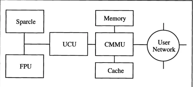
The basic layout of an Alewife node is shown in Figure 1. The Sparcle, an extension of the SPARC architecture [2], serves as the central processing unit. The Communication and Memory Management Unit (CMMU) handles all memory accesses, whether they be local or remote. Message passing and DMA are also handled by the CMMU, which is accessed both explicitly, by memory mapped registers, and implicitly, by loads and stores which the CMMU interprets as shared memory operations.
2.2
Adding Translation and Protection
Because the CMMU is currently designed to understand a globally shared, single address space, upgrading Alewife to Fugu entails placing both the translation logic and the protection logic between the Sparcle and the CMMU. This placement allows the processor to utilize multiple protected virtual address spaces while the CMMU maintains its view of the single coherent physical address space. Of course, if the CMMU maintains coherent memory and caches, the multiple address spaces seen by the Sparcle will also remain coherent.
Similarly, message protection is placed between the CMMU and the Sparcle. Regardless of whether a message is currently deliverable, the CMMU should still receive the message. Because Alewife's network is worm-hole routed, many potential links could become tied up if the CMMU waited. Of course, it is possible that the destination process is not currently running, causing the message to be undeliverable. The potential problem is obvious if any node has two independent processes which are simultaneously polling for messages from the network. The determination of a message's deliverability, then, must be accomplished by logic placed between the CMMU and the Sparcle. Because each group of processes is assigned a unique Group Identification (GID), this message protection logic is called the GID check.
2.3
The Secondary Network
The upgrade to Fugu actually requires one more hardware addition to the Alewife node: a second, system only network. Empirically, it was determined that the user could fill up and deadlock the general system network. Both situations cause the supervisor problems because it cannot send scheduling or other maintenance information between nodes when the system network is full. To correct this problem, a proposed addition for
Fugu is a second network which is only accessible to the supervisor [3, 5]. Briefly, this network has two intended uses: emergency scheduling and overflow paging.
Interestingly, the secondary network does not need to support a high bandwidth. This observation is readily apparent from the intended use of the secondary network. Scheduling information only needs to be sent through the secondary network when the primary system network is busy. Similarly, overflow pages are sent through the secondary network rarely [3].
The low bandwidth necessary will be exploited to make the secondary network primitive as compared to the primary system network. This reduction in throughput capacity will allow for a much simpler and smaller network controller. In fact, it will allow the network controller to share space with the TLB and GID check in a single chip, called the User Communication Unit (UCU).
2.4
The User Communication Unit (UCU)
Much like the TLB and the CMMU, the secondary network must be directly accessible from the processor. As discussed, its purpose is to deliver important scheduling information. Any extra layer between the network and the processor would only hamper the prompt delivery of these messages by increasing latency. Similarly, the GID check must be tightly integrated with the CMMU, the Sparcle, and the TLB.
Because of the similar proximity constraints of the TLB, the GID check, and the secondary network, it would be convenient to package these units together in one chip. In fact, they will be packaged in one processor accessible chip called the User Communication Unit (UCU). The benefits of placing these three modules together can also be seen from a more practical standpoint. This packaging reduces the amount of effort needed to design and debug the Fugu node board.
optimized migration of Alewife to Fugu. If such an implementation of Fugu were made, the TLB would be integrated with the Sparcle, and the secondary network and GID check would be integrated with the CMMU. This difference in packaging would create a much faster node overall as it bypasses the extra delay incurred by accessing an additional chip.
2.5
Fugu's Node Architecture
Figure 2 shows the architecture of the Fugu node. As described, the only difference between the Alewife node and the Fugu node is the addition of the UCU, which includes Fugu's TLB, GID check, and secondary network. The functional specifications of the TLB and GID check are discussed in the sections that follow, and the implementation of the secondary network is discussed in [3].
Figure 2: Fugu node architecture.
3
Functional Specification
Figure 3 shows a block diagram of the UCU, which consists of the TLB, the secondary network, the GID check, and the bus interface. The most important peripheral
modules, the Sparcle and the CMMU, are also shown. Additionally, the secondary network connections are depicted. As will be seen in the sections that follow, these modules combine to provide the basis for a fast, flexible means of user isolation, thus enabling scalable multiuser support.
Although the TLB, GID check, bus interface, and secondary network share many common signals, their specifications will be discussed independently in the sections that follow. This separation is reasonable because of the large differences in the underlying goals of each module. Furthermore, the outputs of each module are conceptually and electrically separate. Note, however, that the bus interface serves as the intermediary for the other modules.
UCU
Figure 3: The blocks contained within the UCU.
3.1
The TLB
In this section, we examine some of the features necessary to meet this goal, such as the translation modes and the programming interface. Special attention will be paid to the translation path, the performance limiting path.
3.1.1 Translation Modes
For the kernel's virtual memory handler to function correctly, it must be continually accessible. If the page handler was swapped out for any reason, a succeeding page fault could never be resolved. One solution to this problem is to disallow swapping of the page handlers. Special, unswappable pages could be marked as such upon their creation. Fugu takes an alternative approach to implementing this functionality by providing three TLB bypass mechanisms: total TLB disable, lower megabyte of address space bypass, and supervisor requested bypass, which includes Alternate Space Identifier (ASI) aliasing. (Section 3.1.4 discusses the purpose of the ASIs.)
When setting up the kernel space or for operating in a single address space, it may be useful to turn off the TLB completely. The TLB supports this disabled mode, in which it simply passes all address untranslated. Additionally, the TLB never translates any address in any context in the bottom megabyte of address space. This feature allows one megabyte of space for all kernel code which must always be accessible.
Finally, certain supervisor ASIs cause translation to be bypassed. The TLB aliases these ASIs to otherwise normal ASIs, although some are treated specially by the CMMU. The purpose of this operation is to bypass the TLB while maintaining normal CMMU operation. It provides the supervisor a means of directly accessing physical memory without needing to find, or even worse, to create, the virtual translation. Table 1 lists the ASIs which are translated as well as the resulting ASI aliases. As can be seen, the aliased ASIs are simply the inputted ASI with the fifth bit set to zero.
ASI range to translate Translated ASI range
0x20-0x3F Ox00-0x1F
0x60-0x7F 0x40-0x5F
Table 1: The ASIs which are translated and the ASIs they translate to.
3.1.2 CID Extension
For a TLB hit in a single address space architecture, it is only necessary that the
tag portion of the memory matches the virtual address presented. In a multiple address
space paradigm, however, it is also necessary that the address be associated with the
currently running group or context (see Section 4.1.5). Therefore, Fugu's TLB registers
the currently running Context Identification (CID). Every time a tag is written to a TLB
element, this CID is automatically appended. For a cache line to hit during translation,
the tags and the associated CIDs must be independently equal.
This procedure allows translations for multiple groups to coexist in the TLB. In
other words, TLB entries do not have to be invalidated when the context switches.
Because the TLB does not have access to the currently running CID, however, the
supervisor must update this register on every switch (see Appendix 1.1). Fortunately,
updating the CID register is much less expensive than invalidating all TLB entries,
especially if some TLB entries are utilized after their contexts have been swapped back
in.
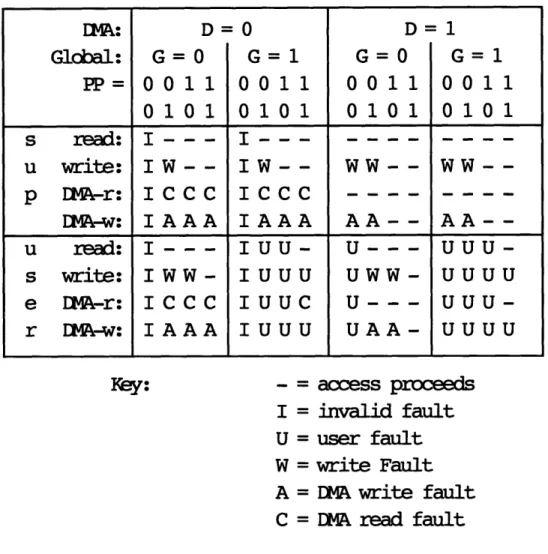
3.1.3 Protection and Faults
In a multiuser machine, protections are a key part of system stability. For example, some addresses should be marked as only assessable to the supervisor. For performance
optimization, the TLB actually performs these protection checks in parallel with translation. The TLB maintains four protection bits for every entry. Collectively called DGPP, they define the full access control for the address. The D bit actually has a second purpose: it is the "DMA-able" bit and indicates whether DMA operations may be performed on an address. The G bit is named the "Global" bit for historical reasons. The PP bits form the Protection field, although all four bits really combine for this purpose. Table 2 lists all possible access combinations.
To make use of the information presented in Table 2, the TLB must know whether the current operation is a read or write, at user or supervisor level, or for DMA. This knowledge, combined with the four protection bits, combinationally produces a three bit fault code. The possible input combinations are listed in Table 3 and the possible fault codes are listed in Table 4. Note that the fault generation logic produces the three bit
Table 2: The access permitted for each combination of the DGPP bits. RO means read only and R/W indicates both read and write access. DMA transactions require the D bit to be set.
D=0 D=I
G P P user super user super
0 0 0 invalid - RO 0 0 1 RO RO RO RO 0 1 0 RO R/W RO R/W 0 1 1 R/W R/W R/W R/W 1 0 0 invalid - RO 1 0 1 - RO - RO 1 1 0 - R/W - R/W 1 1 1 RO R/W RO R/W
Key:
access proceeds
invalid fault
user fault
write Fault
DMA write fault
IMA read fault
Table 3: The faults associated with specific accesses and protections. The bits stored in the TLB are specified horizontally while the bits derived from the current operation are specified vertically.
sequence 111 when no fault is present. This allows a simple three input and gate to
produce the "no protection fault" signal.
Maintaining protection violations isn't quite as straightforward as one might think.
Because the Sparcle is a pipelined processor, many different faults are possible from all
instructions currently being processed. For example, one instruction might be writing to a read only page while the next instruction attempts to read from a page which is not currently loaded in the TLB. To maintain consistency with the order of faults serviced,
EMA:
D
=
0
D=
1
Global:
G=0
G=
G=0
G
= 1
PP=
0011 0011
0011 0011
0101 0101
0101 0101
s
read:
I---
I---u write: IW-- IW--
WW--p
IMA-r: ICCC ICCC
IMA-w: IAAA IAAA
AA--u
read: I--- IUU-
U---
UUU-s
write: IWW- IUUU
UWW- UUUU
e IEMA-r: ICCC IUUC
U
- - -
UUU-r EMA-w:
IAAA IUUU
UAA-
UUUU
Table 4: The fault codes.
the TLB only maintains the first fault seen after the last probe for faults. Additionally,
whenever the TLB is probed for a fault code, it clears the stored fault code. This
procedure allows the kernel to more easily differentiate between TLB related faults and
other unrelated faults.
The TLB actually causes a trap by forcing the CMMU to cause a trap. The TLB
emits a physical address with the four high order bits set to the hexadecimal value Oxl,
which maps to shared memory on nonexistent processors. These addresses causes the CMMU to trap the Sparcle. Kernel code can then probe for the cause of the trap (see Appendix 1.6).
3.1.4 Interconnecting The TLB, The Sparcle, and The CMMU
The Sparcle instruction set provides an 8 bit Alternate Space Identifier (ASI) with every address. In Fugu, these ASIs have many uses, such as distinguishing between supervisor and user accesses. The TLB makes use of several ASI's for its own internal operations. As presented in Section 3.1.1, the TLB also has the ability to change the ASI on its way to the CMMU. From the above discussion, it follows that the TLB must
Code Fault 0 Refill
1 Invalid 2 Write Fault
3 User Fault
4 DMA Write Fault
5 DMA Read Fault 6 Undefined 7 No Fault
receive the virtual address and ASI buses from the Sparcle and provide the physical
address and ASI buses to the CMMU. For protection operations, the TLB also makes use
of two Sparcle signals: one which specifies a read operation and one which specifies a
supervisor operation.
UCU operations (discussed in Section 3.4) involve complex interplay between the
Sparcle, the UCU, and the CMMU. While the purpose of these signals is discussed in
Section 4.4, it is noted here that the UCU also makes use of the following signals: The
Sparcle's supervisor bit as an input, the CMMU's supervisor bit as an output, the CMMU's
sigoe signal as an input, the CMMU's regAck signal as an input, and the CMMU's
regHold signal as an output. Essentially, these signals combine to provide a sophisticated
handshaking scheme between the three chips.
3.2
The GID Check
3.2.1 Background
For complete user isolation, messages as well as memory references must be protected. As one might expect, there are many ways to accomplish this goal. For example, the kernel could be trusted to check the destination of all messages and then ensure the correct distribution of these messages. Unfortunately, this method requires a lot of overhead. Unless the supervisor is currently running, there are a minimum of two context switches to implement this solution: one to load the kernel and then one to load the receiving process. Furthermore, the kernel might have to buffer the message, which
requires copying the message at least twice before it is received.
Alewife was designed to avoid this overhead by allowing the user process direct access to the network hardware. Although extra precautions must be taken to ensure forward progress under this scheme, it is clear that this method will increase performance
dramatically under the optimal case, when the receiving process is running and ready to receive. Fortunately, it has been determined that the optimal case is also the usual case [5]. Therefore, this method increases performance dramatically.
Unfortunately, maintaining protection under this situation is difficult. The network hardware must ensure that the proper process is running before beginning delivery. Furthermore, unless sufficient network buffer space is preset, there must be some mechanism for buffering the network data when the incorrect process is running. If the message is allowed to stay in the network for too long, the network might fill up and block.
3.2.2 Operation of The GID Check
The GID check supports these two necessary mechanisms, delivery protection and network saturation protection, by imitating the network hardware's message polling protocols. In Alewife, polling for a message is accomplished by reading from a memory mapped address. If a message is present, the CMMU will return the message header and set Alewife's full bit. If no message is present, the data returned is undefined and the full bit is cleared.
With this protocol in place, the GID check simply snoops for a load of this memory mapped location. After a load of this location has been detected, the full bit is checked. If the full bit is low, then the GID check passes all signals unaltered. Similarly, the virtual supervisor bit is checked. If the Sparcle is currently in supervisor mode, then all signals are passed unaltered. The remaining case, of course, is a message waiting during a user load. In this case, the GID check verifies that the destination GID included in the header matches the currently loaded GID in the UCU's GID register. If the GID matches, then all signals are again passed unaltered; the protection check has passed. However, if the GID does not match, the GID check forces the full bit clear, causing the polling process to continue as if no message has arrived. Additionally, the GID check
interrupts the Sparcle and the CMMU via the external interrupt signal. This causes a
special kernel handler to be run which properly empties the message into a buffer.
The performance benefit of this procedure is clear if the destination GIDs are
usually running when their messages arrive. Fortunately, it has been determined that this
is the common case. The expensive kernel control described above is rare, and thus there
is a great performance benefit realized by adding the hardware GID check.
3.3
The Secondary Network
The secondary network provides a low bandwidth backup for the main system
network. The motivation and implementation of the secondary network are discussed in
[3]. Section 4.3 describes the programming interface for the secondary network.
3.4
The Unified Programming Interface
For proper UCU functionality, many registers must be updated. For example, the
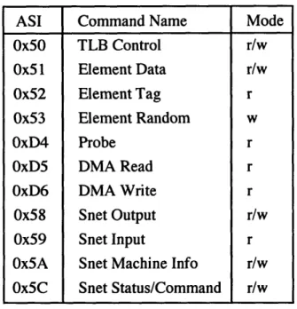
virtual tags and physical translations must be written to the TLB's memory. Similarly, when TLB related faults occur, the kernel must be able to find the cause by probing the TLB. For these and other functions, the UCU has its own instruction set. All instructions are specified by special ASIs, which are listed in Table 5. Note that the last four instructions are for the secondary network. These instructions, as well as a couple listed instructions
which have side effects for the GID check, are fully described in Appendix 1.
Interestingly, the programming interface for all three UCU modules is unified. All UCU operations are accessed via "colored" Sparcle loads and stores. A "colored" load or store is one which has a special Alternate Space Identifier (ASI). These special ASI's are recognized by the UCU bus interface and cause a special sequence of events (see section 3.5).
Due to the unified nature of the programming interface, it is convenient to place its logic in one module. Doing so makes sense from a design point of view because it
eliminates redundant logic. Furthermore, distributing control among all modules reduces
performance because multiplexers are required at the outputs. Because a relatively slow
technology is being used to implement the UCU, any extra performance gain is welcomed.
3.5
The Bus Interface: The XROM Space
The UCU bus interface is quite simple during a normal translation operation. The
virtual address bus is an input to the UCU, and the physical address translation is an
output. The offset bits are unchanged by the UCU, and as such, are bypassed on the
printed circuit board.
UCU loads and stores, however, are slightly more complicated. As mentioned- in
section 3.4, the UCU recognizes these operations by special ASIs, which are listed in
Table 5. When a special ASI is spotted, the UCU must make sure that only it and the Sparcle have control of the address and data buses. If the CMMU or cache still had
control, for example, contention would result. Furthermore, to simplify the logic necessary for the UCU's bus interface, it would be convenient if UCU operations progressed with an uninterruptible sequence of cycles. Because of the possibility of cache misses and remote message arrivals, this type of atomic sequence of cycles is extremely hard to guarantee.
Fortunately, the CMMU has an interface for handling this type of situation. Namely, an external memory (XROM) access causes the CMMU to finish all outstanding transactions and then ready for an atomic sequence. Any other unexpected and possibly asynchronous events are queued until the XROM access is over. The UCU makes extensive use of the XROM space to greatly simplify its bus interface.
Table 5: The TLB instructions.
4
Implementation
Although all three main sections of the UCU have been developed separately, there are a few underlying similarities. For example, the bus interface, which is discussed in Sections 3.5 and 4.4, is unified. Additionally, all components of the UCU have been written in Verilog. The Verilog code is merged together and compiled for a single FPGA (see Section 5).
Specifically, the UCU is implemented with a Xilinx 4025 for a few reasons. 1) The 4025 supports distributed placement of SRAM, which is important for the TLB. 2) The 4025 is deemed to be one of few FPGAs currently on the market which is large enough to fit the UCU. The 4025 has both sufficient gate count and sufficient SRAM capacity. 3) Xilinx continues to evolve this series of FPGAs. Bigger and faster 4000 series chips will be available in the future, potentially enabling much larger and faster TLBs and higher bandwidth secondary networks.
ASI Command Name Mode 0x50 TLB Control r/w 0x51 Element Data r/w 0x52 Element Tag r 0x53 Element Random w
OxD4 Probe r
OxD5 DMA Read r
OxD6 DMA Write r
0x58 Snet Output r/w
0x59 Snet Input r
Ox5A Snet Machine Info r/w Ox5C Snet Status/Command r/w
4.1
The TLB
In this section, we examine the design of Fugu's TLB. Some design parameters,
such as the 32 bit virtual and physical address spaces, have been imposed by the Alewife
architecture. Other parameters have been tuned to meet the needs of Fugu.
Section 4.1.1 describes the overall organization of the TLB. Section 4.1.2 details
a generic translation path commonly used for a single column of a TLB while the
remaining sections examine the extensions and enhancements used for Fugu. The parameters
of the TLB are summarized in Table 6.
Table 6: The TLB column organization.
4.1.1 The Overall TLB Architecture
The overall architecture of the TLB is shown in Figure 4. During normal operating
modes, the translation path is active. It is purely combinational, which is necessary due
to the timing constraints of the Sparcle processor. Sparcle emits a valid virtual address
before the positive edge of the clock. The virtual to physical address translation must also be complete before the same positive edge of the clock.
During translation, the memory cells are controlled by the inputs from the Sparcle.
However, when a special TLB operation is recognized (see Appendix 1) by the "Op Logic" shown in Figure 4, a state machine assumes control of the memory cells. This
Virtual Address Size 32 bits Physical Address Size 32 bits Page Size 4 kilobytes TLB Organization 4-Way, Set Associative Entries Per Column 32
state machine is depicted by the Read/Write logic in Figure 4, and it ensures correct
completion of the requested function, while maintaining the correct bus interface. The
UCU's unified bus interface overlaps with this block.
The TLB has been implemented in the Verilog hardware description language.
This code implements the functionality discussed previously and developed in the following
sections in a straight forward manner with one exception: the SRAM, which uses hard
macros. The macros are termed hard macros because they are defined in Xilinx's proprietary
XNF format and not in the Verilog language. The Xilinx program memgen is used to
generate these macros. It is believed that memgen generates efficient SRAM with respect
to both time and space.
Virt. Adc From Sp, Controls From Sparcle Data To and Fron Sparcle
Figure 4: Overall TLB organization.
4.1.2 A Generic TLB Translation Architecture
Figure 5 shows a generic translation architecture for a single set of a basic multiple set associative TLB. Although Fugu's TLB extends this architecture, it is presented first for clarity. Fugu's enhancements are discussed in Sections 4.1.3 through 4.1.6.
The set shown in Figure 5 contains two equally deep sections of memory. One section stores the tag, which is used to determine the contents of the TLB's entries. The second memory section contains the physical address translation.
The low order bits of the Virtual Page Number (VPN) are used to index into both sections of memory. The number of bits used is determined by the depth of the sections of memory; in the current implementation of Fugu's TLB, the memories have 32 entries, and thus the 5 low order bits of the VPN are used for the index. For the determination of the depth of the memory cells, see Section 4.1.3.
A Single Column of a Basic TLB
VPN[4:0]
DDR Bus
Figure 5: A basic TLB organization. The memory cells are equally deep and in this case equally wide.
The tag is formed by the high order bits of the virtual page number (see Section
4.1.4 for the determination of the page size, and thus the amount of bits remaining for the
VPN). Specifically, the tag bits must uniquely specify which virtual page number resides
in the TLB. Because the 5 low order bits of the VPN are already specified by which
memory locations the TLB accesses, only the remaining 15 high order bits of the virtual
page number must be stored in the tag section of the memory.
When a virtual address is presented to the TLB, the memories indexed by the low
order bits of the VPN are examined. The contents of the tag sections of each set are then
simultaneously compared to the top 15 bits of the supplied virtual page number. If the
contents of the tag memory from any of the sets equals the supplied VPN, that set has a
TLB hit. The translation stored in the Physical Page Number (PPN) memory of that set is
placed on the outgoing address bus. If no set hits, a TLB refill trap is placed on the
address bus (see section 3.1.3). It is up to the refill code of the supervisor to ensure that
identical tags are not placed in more than one set.
4.1.3 Depth of the Memory Sets
Xilinx SRAM cells are packed efficiently only when they store a multiple of 16 bits. Any other storage size will cause wasted Combinational Lookup Blocks (CLBs), the basic logic generators in the Xilinx architecture. Because the CLBs are in limited supply, they should not be wasted. Since the width of the memory cells of the TLB are not multiples of 16 bits, the memories are made 32 entries deep. This depth allows efficient memory packing no matter how wide the SRAM cells are. Of course, the sets could just as easily be made 48 entries deep without any loss of CLB utilization. Section 4.1.5 will show that this depth is undesirable because the extra SRAM could be better utilized in a more highly associative cache. Furthermore, a depth of 16 is undesirable because of the extra bussing required for the extra sets of memory present.
4.1.4 Page Size
A virtual address actually contains two portions: a virtual page number and an
offset. To exploit the spacial locality of program references, thereby reducing the amount
of memory swapping necessary, virtual memory is actually swapped in contiguous chunks
of address space called a page. The offset portion of the virtual address specifies an
index into a virtual page, which is specified by the VPN.
When virtualizing memory, an important question is how large to make the pages.
A large page could reduce the amount of page swapping necessary. The larger the page,
however, the larger the penalty incurred upon swapping, especially if the page resides on
a remote node. A page size of 4k (12 bits) is chosen for Fugu because it is a nice balance
between these two constraints. Interestingly, it is on the small side of the page sizes
commonly used for distributed shared memory machines.
Because the TLB only needs to translate the virtual page numbers and not the
offsets within the page, the TLB is only concerned with translating the top 20 bits of the
32 bit virtual address. During ordinary translation operations, the bottom 12 bits simply pass through the TLB. Alternatively, as implemented with Fugu, the offset bits could be bypassed on the printed circuit board.
4.1.5 Associativity
Another important design consideration is the associativity of the TLB. For a given amount of memory, the TLB could either be deeper (more entries per set) or more associative (more sets). The deeper cache works well in a single context situation. Unfortunately, when the context switches, most memory references will have to be reloaded into the cache. It is important to remember that to simplify process launching, most of the processes will be running in the same general ranges of virtual address space. Thus,
if every process needs to access the contents of their virtual memory location 100, every
context switch should cause a miss and reload of location 100. Very commonly, TLBs
invalidate every entry when switching contexts. This prevents the TLB from computing
improper translations. Fugu's TLB, on the other hand, keeps track of which context a
valid tag belongs to (see Section 3.1.2). This prevents the TLB from having to invalidate
every entry upon every context switch.
Even though Fugu's TLB entries need not be invalidated upon every context
switch, there is another problem. The general TLB translation architecture presented in
Section 4.1.1 only provides as many spots for any given virtual address as there are sets
in the TLB. These spots must be shared among all processes requiring the same and
other potentially overlapping addresses. (Addresses overlap spots in the TLB when the
bottom five bits of their VPNs are equal.) Thus, processes running in the same virtual
address ranges will tend to overwrite other processes' TLB entries. If this entry elimination
occurs at every context switch, performance is not much better than that seen if every
TLB entry is invalidated upon every context switch.
An approach around this second multiple context problem is to index the cache
not just by the lower bits of the VPN, but also by the context ID. In general, there are many hashing functions which could be used to compute the index. In Fugu, the entries are indexed by the lower 5 bits of the VPN logically XORed with the lower 5 bits of the CID. The XOR function was chosen because of its simplicity and its effect of locating the same VPN from adjacent groups on as many different cache lines as possible.
While indexing the cache as described does tend to move different processes' addresses onto different cache lines, it still does not solve the cache line collision problem. Quite simply, increasing the associativity of the cache reduces this problem. The other problems presented in this section are also reduced as the associativity of the TLB rises. Unfortunately, the Xilinx architecture limits the amount of associativity which can be utilized efficiently. As discussed in section 4.1.3, it is undesirable to lower the depth of
the sets below 16 entries, which limits the amount of associativity available. In fact, the
degree of associativity chosen is equal to the number of sets which are believed to fit in
the Xilinx 4025 using 32 entry sets.
4.1.6 Putting It All Together: The TLB's Translation Path
Figure 6 shows the overall translation path of the Fugu TLB. While it shows only
a single set of the TLB, it depicts most of the functionality presented to this point,
including the CID section of the tag memory, the protection bits, and the fault generation
logic.
4.2
The GID Check
Section 3.2 describes the functionality of the GID check. This section clearly
defines the implementation of the GID and then shows an example of the GID check.
4.2.1 Definition of The GID
Before discussing the implementation of the GID check, a few key terms must be clearly defined in terms of the UCU's implementation. The Context ID, or the CID, is an ID for all processes local to a node. All unique virtual address spaces have a unique CID. If local processes share the same CID, then they are operating in the same virtual address space. The Group ID, or the GID, however, is assigned to distributed processes. In other words, processes with an assigned GID are operating within the same virtual address space on more than one node.
Fugu's CIDs are 8 bits wide, which permits 256 unique, local, virtual address spaces. Due to message header constraints, however, Fugu's GIDs are limited to 7 bits,
A Single Column of the FUGU TLB
VPN[1
Supervisor
Write DMAOp?
Figure 6: The overall translation path of the Fugu TLB. This figure depicts one set of a multi-set TLB.
which allows for 128 unique, distributed processes. By definition, these distributed processes should reside in their own virtual address spaces. Although it might be necessary to allow for more than 128 global process IDs, it is hypothesized that 128 unique local
processes per node is sufficient for Fugu.
Therefore, to reduce complexity, both the CID and the GID actually share the
same register in the UCU. The GID is defined as the lower 7 bits of the CID register.
Further, a CID with the high order bit set is defined to be a local process while a CID
with the high order bit cleared is defined to be a GID whose GID is equal to the lower 7
bits of the CID register.
4.2.2 An Example of The GID Check
Figure 7 shows the GID check in action. It is the output of test vectors applied from a Verilog test program. The first trace is the clock signal upon which all synchronous logic is generated. The second trace is the state of the testing machine. The remaining traces are, in order, the virtual address bus (aBusIn), the physical address bus (aBusOut), the virtual ASI bus (asiln), the physical ASI bus (asiOut), bits 17 through 23 of the data bus ([23:17]), the virtual supervisor bit (suln), the full bit from the CMMU (cccOin), the full bit emitted to the Sparcle (cccOout), the GID (GID), and finally, the IRQ request from the GID hardware (gidIrq). Bits 17 through 23 of the data bus contain the destination GID when a message header is read. To reduce Figure 7 to the interesting parts of the GID check, the reset states are not shown. Furthermore, the TLB is enabled and the CID is set to 0x04, which is not shown.
A GID check begins in State 6. In this state, the special ASI OxcO is presented with the special offset address of 0x080. The GID Check recognizes this address and will be watching the data bus, the supervisor bit, and the full bit on the next cycle. If the full bit is not set, then there is no message waiting, and the GID check does nothing. Similarly, if the supervisor bit is high, then the kernel is currently running, and all messages are deliverable. Hence, the GID alters nothing.
2 a v
I
3I
Figure 7: An example of the GID check.
i
t1
LJJ"i
__ I II
!
Therefore, a message is waiting during a user level probe. For this reason, the GID check
matches the GID in the destination field of the data bus (bits 17 through 23) with the
lower 7 bits of the CID register. In this case, the GID matches, and so the GID Check
passes all signals unchanged. This determination is done combinationally, which causes
the full bit that the GID Check outputs to the Sparcle to be undefined while the data bus
is undefined. This period of uncertainty poses no problems because the full bit from the
CMMU is also undefined at this time.
State 8 shows another message header probe. This operation looks identical to
that shown in state 6. However, in state 9, it can be seen that the GID returned by the
CMMU does not match the GID stored in the UCU. Because of the mismatch, the GID
check combinationally forces the full bit (cccOout) to 0. In order to meet the timing
model for the upcoming branch on full instruction, the UCU actually holds the full bit in
the empty state through an additional positive edge. With this procedure complete, it will
appear to the running process that no message is waiting in the network buffers.
Although the GID check has now successfully protected the message interface, the kernel should be made aware of the waiting message so that it can free the network resources. Therefore, at the positive edge following the realization of the mismatch, the GID check asserts its IRQ request line. The IRQ will cause an external interrupt, which will force a kernel handler to be run. Although the kernel should free the message from the network hardware at this point, there are many other additional actions which the kernel might take.
4.3 The Secondary Network
The implementation of the secondary network is described in [3]. However, in
this section, we make note of a few implementation details about the secondary network bus interface.
As discussed in Section 3.4, the UCU interface has been unified into a single
module. Therefore, many of the secondary network registers are actually maintained
within the bus interface. These registers are read and written exactly as any other UCU
register would be.
However, there are some registers, such as the input and output buffers, which are
located in the secondary network module. With these registers, there is the unfortunate
possibility of usage contention between the UCU interface and the secondary network
itself. To avoid this problem, there is a handshaking scheme in which data read from the
secondary network is presented on the second positive edge following the request. In
order for this to work, the UCU must assert regHold to stall the XROM read operation
one cycle. For secondary network writes, however, the handshaking scheme does not
create any problems; these write operations proceed exactly as they would for the TLB's
registers.
4.4
The UCU Bus Interface: The XROM Space
As discussed in Section 3.5, the UCU makes extensive use of the CMMU's XROM space in order to simplify bus operations. This section describes the implementation of the XROM space. Section 4.5 will show examples of the usage of the XROM space.
Much like most other CMMU operations, the XROM space is a supervisor level, memory mapped access. It is defined to be addresses with the 4 high order bits set to 0x6. To ensure that the XROM access occurs at supervisor level, the supervisor bit must be set during the cycle following the positive edge that the address is valid. The Sparcle defines this placement of the supervisor bit, which the CMMU and UCU must honor.
Furthermore, a supervisor ASI must be emitted along with the XROM address. Although perhaps counterintuitive, setting the supervisor bit is not sufficient to define a supervisor access because roughly half of the ASIs are defined at user level. Any of the
remaining ASIs, which, of course, are defined at supervisor level, should work. Therefore,
the UCU uses the supervisor ASI OxOb during bus operations.
To summarize this discussion, the UCU does three things when a special ASI is
detected. First, it combinationally emits a physical address with the 4 high order bits set
to 0x6. Second, it combinationally sets the ASI to OxOb. Third and finally, it ensures that
the supervisor bit is high during the next cycle.
Upon completion of this procedure, the CMMU will log the XROM request. An
indeterminate number of cycles later, the CMMU will grant the XROM request by raising
the regAck signal. In the common case, regAck will be raised during the same cycle as
the XROM request has been made. There are many situations, such as cache refills,
which could delay the start of the XROM operation any number of cycles.
Once regAck is raised, only one of two possible sequences of cycles is run next.
A read operation will result in one sequence of events while a write operation will result
in the other. Both of these sequences begin the first positive edge that regAck is high. It is important to reiterate that nothing, including external interrupts, can stall either of these sequences once they have begun.
If the operation is a write, then the data to be written to the UCU comes from the Sparcle and will be valid surrounding the next positive edge of the clock. With no UCU intervention, the next address to be translated will be presented before the next positive edge following the appearance of the data.
Because of setup and hold time constraints, this brief presentation of the data may not be long enough for proper handing within the UCU. Therefore, under certain circumstances, the UCU raises another CMMU signal called regHold which will extend the write cycle. RegHold is raised just following the positive edge in which the data is presented and must be held high throughout the remainder of the cycle. After the UCU lowers regHold, the data from the Sparcle will become invalid. Furthermore, the address of the next operation will be emitted before the next positive edge. Of course, the UCU
must properly handle this address.
Read operations function similarly to writes. The UCU provides the requested
information on the positive edge following the positive edge in which regAck has gone high. To ensure that the UCU meets the setup and hold times of the Sparcle, the UCU
actually emits the data from the previous negative edge until the following negative edge.
This procedure is allowable because the CMMU has ensured that there is no other bus
driver during either of these two cycles. They are reserved as the so called "bus turn
around" cycles.
As with writes, the UCU can stall the read process by asserting regHold. Again,
regHold must be asserted just past the positive edge in which the data was to be presented
to the Sparcle. Assertion of regHold must continue throughout the rest of the cycle. The
UCU then drops regHold just past the positive edge in which it has written the data. At this point, the operation will complete as if regHold had not been raised. In other words, before the arrival of the next positive edge, the Sparcle will emit the address of the next operation.
4.5
An Example of The UCU Bus Interface
The UCU bus interface is similar for all UCU reads, as is the interface for all UCU writes. This section discusses one such UCU read, one such UCU write, a typical translation operation, and a TLB fault. The specifics of all UCU instructions are discussed in Appendix 1. Furthermore, the XROM interface used for UCU reads and writes is described in Section 4.4.
Figure 8 shows the signals used to interface between the Sparcle, CMMU, and UCU. In these traces, the Sparcle and CMMU are simulated by a testing state machine written in Verilog. The first trace is the clock whose edges are used to synthesize all synchronous logic. The second trace shows the state of this simulator. The remaining
traces, in order, are the virtual address bus (aBusIn), the physical address bus (aBusOut), the virtual ASI (asiln), the physical ASI (asiOut), regAck, regHold, readProc (high if the current operation is a read), the virtual supervisor bit (suln), the physical supervisor bit (suOut), and finally, the data bus (dBus).
In order to eliminate the uninteresting states of the simulation shown in Figure 8, a few important cycles have been left out. Namely, the missing states reset the UCU, enable the TLB, and set the current CID to 4. Clearly, these instructions are necessary for the correct functionality of what follows.
An Element Data Write command begins in state 6. The UCU recognizes this operation by it's special ASI, 0x51. Combinationally, the UCU emits a physical address with the 4 high order bits set to 0x6 and an ASI of OxOb. Furthermore, the UCU ensures that the supervisor bit (suOut) is high during the next cycle. This procedure imitates the external memory (XROM) space of the CMMU, which is discussed in Section 4.4. Shortly after the CMMU latches the XROM request at the positive edge of the clock, the CMMU marks the beginning of the XROM access by raising the regAck signal. The UCU notes this information at the first positive edge of the clock in which regAck is high.
The UCU expects the store data to be valid at the following positive edge. Because this data is being written into Xilinx memory cells, the Xilinx setup and hold times must be met. In order to meet these requirements, the UCU asserts regHold for three cycles, which will keep the data valid for the same three cycles. The first cycle is used to meet the setup time while the second cycle is used to write the data. Finally, the third cycle is used to ensure that the hold time is met. As can bee seen in Appendix 1.2, the data written is a physical page number translation of OxI lIa for virtual page number Ox100. Furthermore, the protection bits (DGPP) are set to Oxb.
Next, at state 8, the correct translation of virtual page number Ox 100 is seen. The physical page number Oxl 1 la is sent to the CMMU via the physical address bus aBusOut.
Figure 8: A TLB write, translate, and read operation. The waves shown are those used to interface between the Sparcle, CMMU, and TLB.
I I to I0 ---~·-rrrr ~-~~~- --w ! •mmi r DI1~wrrr
The offset bits, in this case 0x120, are passed unchanged.
Beginning at state 9, the test code probes for the previously written translation via
a Probe Read command (see Appendix 1.6). As can be seen in Figure 8, the XROM
interface is imitated exactly as before. Again, the UCU waits for the next positive edge
during which regAck is raised. Once this condition is met, the UCU must provide the
necessary data bus data on the following positive edge. To ensure that the data is valid
long enough surrounding the edge to meet all setup and hold times, the UCU actually
provides the data all the way from the previous negative edge to the following negative
edge. Because this procedure is extremely conservative, it guarantees that the setup and
hold times are met.
Interestingly, the Sparcle presents the virtual address of the next operation during
the same positive edge that the UCU places data on the data bus. Although it may seem
that this sequence forces the TLB to be translating while presenting data bus data, the
address is actually nullified by the Sparcle. Therefore, it does not matter what physical address is emitted during this cycle.
State 12 presents the final type of "normal" UCU operation, a fault. During this cycle, the virtual page number 0x200 is presented to the TLB. This VPN has not been loaded in the UCU and therefore causes a TLB Refill Fault. The UCU causes all faults by combinationally supplying a physical address with the 4 high order bits set to Oxl. The CMMU will then cause a kernel handler to be run. This handler probes the UCU to learn cause of the fault (see Appendix 1.1).
5
Methodology
Figure 9 shows the design methodology used for the UCU. Various representations of the UCU are boxed while the tools necessary to generate these representations are circled. As can be seen in the right hand column of Figure 9, the design flow begins with
Design Flow
Figure 9: The design methodology used for the UCU. Representations of the UCU are shown boxed while tools used to generate these representations are shown encircled.
the Verilog description of the UCU and ends with the Xilinx implementation.
Unfortunately, the only way to test the Xilinx implementation is to run it on a Fugu node board. No simulator is capable of testing all of Fugu's chips in their intended
technology representations. This desired but unavailable simulator is called the "Ideal
simulator" in Figure 9.
Because Fugu node boards have not yet been built, the UCU has been tested in
two alternative representations: the original Verilog representation and an LSI gate level
representation. These tests form the remainder of Figure 9 and will be discussed in the
sections that follow. However, the design flow for the intended Xilinx representation is
described first.
5.1
Compiling the UCU for Xilinx
The design flow for the Xilinx implementation of the UCU is shown in the right
hand column of Figure 9. First, the Verilog code is compiled to Xilinx gates with Synopsys. The output of Synopsys is run through XACT, which includes Xilinx's automatic place and route tool, called ppr. Before ppr can be run, however, the design is floor planned. Specifically, the memory cells in the TLB are placed in a logical structure so that ppr will properly recognize and implement buses. The output of XACT is a bit stream which can be downloaded directly onto the 4025 via the XChecker cable, another Xilinx tool.
5.2
Verilog Testing
An obvious method to debug the UCU is to simulate the source file. Therefore, the UCU has been tested for functionality at the Verilog level. Test vectors were created
to verify all functional operations of the UCU. Figure 7 and Figure 8 are examples of such test vectors. Through this testing process, all known behavioral bugs have been eliminated.
than will actually be used. To efficiently pack memory onto the Xilinx array, Xilinx hard
macros are utilized. These hard macros have no Verilog model, and therefore cannot be
simulated. Thus, a Verilog model of these hard macros has been created. Care was taken
to match the data book description of the macros as closely as possible. For this reason,
substituting the models should not cause any problems.
5.3
Node Level Testing
The Verilog simulation discussed in Section 5.2 essentially tests the UCU in isolation. No accurate Verilog models exist for the UCU or for the Sparcle. Hence, they
have been approximated in these tests. The next logical step, of course, is simulation
with better models for all surrounding chips. To accomplish this goal, there are a few
options. The most obvious choices are to write better Verilog models for the rest of the
node or to utilize the gate level simulator already present for Alewife.
Neither of these options is straightforward to implement. It would be a complicated
task to rewrite the CMMU and Sparcle in Verilog. This process is prone to errors and
therefore would have marginal success, at best. For this reason, it is desirable to utilize the existing gate level simulator of Alewife. If the UCU could be plugged in somehow, a
reliable simulation should result.
Unfortunately, the Alewife simulator, called NWO, has no facility for adding Verilog modules. It can only utilize Behavioral Syntax Language (BSL) modules or LSI 100k gate level modules. Rewriting the UCU in BSL has the same problems as rewriting the CMMU in Verilog; this process would be error prone because it is not automatic. However, Synopsys automates Verilog to LSI 100k translation, much as it automates Verilog to Xilinx translation. Therefore, Synopsys is used to target the UCU to the LSI 100k series gate arrays. The only translation which cannot be automated is that of the Xilinx memory macros. For simulation of these macros, BSL modules are written and
substituted. Clearly, testing the UCU at the gate level is desirable because it is a step closer to testing the intended Xilinx implementation (see Figure 9).
Once the LSI translation has taken place, the UCU is plugged into NWO, and Sparcle assembly test vectors are written. The Sparcle test code used is quite extensive and tests as much of the functionality of the UCU as possible. Furthermore, the code is self-checking and will display error messages when failures are detected.
Throughout this testing process, many more bugs were found. Most of these bugs involved the specific timing constraints of the bus interface, which could not be tested accurately in the Verilog simulation. Furthermore, there were a few bugs involving instances during which the CMMU spontaneously takes control of the buses. These cases could not be foreseen during the Verilog testing. Regardless of the nature of the bugs found, all that are known have been eliminated.
5.4
Untestable Issues
Unfortunately, successful testing at the Verilog and NWO levels does not ensure correct operation on the 4025. There are many reasons for this unfortunate consequence. The primary concern is the Xilinx memory macro which could not be tested at either level. While the functionality of these macros is specified by the Xilinx manual, it was empirically found that the real world performance of a relative of the 4025, the 4005, was not always equivalent to that predicted by the manual. Because we cannot yet test on a 4025, it is unknown how the SRAM macros will perform for Fugu.
Furthermore, timing is extremely variable on Xilinx FPGAs. There are significant delays incurred by the CLBs and the routing mechanisms on the chip. Every time the design is routed with ppr, it is routed differently. This uncertainty leads to unpredictable timing, which usually poses little problem, except for the SRAM macros and for the tri-state buses. Fugu attempts to fix the SRAM setup and hold time problem by being
extremely conservative during write operations. Additionally, to lessen the chances of
glitches on the write enable signals, they are taken directly from flip-flop outputs. Fugu
eases the tri-state bus problem by only enabling tri-state buses during the second half of
the clock. The tri-state enable signals are allowed to settle during the first half of the clock, thereby lessening the chances of contention during the second half of the clock.
Of course, this process reduces performance because the second half of the clock is mostly wasted. Due to the size of the buses involved, it is impractical to use multiplexors instead.
6
Performance
Although the UCU cannot yet be tested on its intended target, the Xilinx 4025,
much effort has been spent on predicting its performance once downloaded onto a 4025.
Many smaller versions of the UCU were tested on a smaller relative of the 4025, the 4005 [6]. These studies predicted that the translation path propagation delay of the UCU
would be between 155.5 and 186.6 ns when running on a 4025 with Xilinx speed grade -4. Shortly, it will be seen that this prediction was extremely accurate, even though direct comparison is difficult.
6.1
Methodology of The Past Prediction
The performance prediction discussed in [61 was made by comparing the real world performance of 4005 circuits with that predicted by XDelay, Xilinx's timing analysis tool. These comparisons showed that XDelay was conservative in its estimates, and that the real world performance was about two thirds of XDelay's predictions. To arrive at the prediction for the UCU's propagation delay, this two thirds correction factor was