RESEARCH OUTPUTS / RÉSULTATS DE RECHERCHE
Author(s) - Auteur(s) :
Publication date - Date de publication :
Permanent link - Permalien :
Rights / License - Licence de droit d’auteur :
Bibliothèque Universitaire Moretus Plantin
Institutional Repository - Research Portal
Dépôt Institutionnel - Portail de la Recherche
researchportal.unamur.be
University of Namur
Application of a genetic algorithm in four-terminal perovskite/crystalline-silicon tandem devices
Razzaq, Arsalan; Mayer, Alexandre; Depauw, Valérie; Gordon, Ivan; Hajjiah, Ali; Poortmans, Jef
Published in:
IEEE Journal of Photovoltaics DOI:
10.1109/jphotov.2020.3025768 Publication date:
2020
Document Version Peer reviewed version Link to publication
Citation for pulished version (HARVARD):
Razzaq, A, Mayer, A, Depauw, V, Gordon, I, Hajjiah, A & Poortmans, J 2020, 'Application of a genetic algorithm in four-terminal perovskite/crystalline-silicon tandem devices', IEEE Journal of Photovoltaics, vol. 10, no. 6, 9217594, pp. 1689-1700. https://doi.org/10.1109/jphotov.2020.3025768
General rights
Copyright and moral rights for the publications made accessible in the public portal are retained by the authors and/or other copyright owners and it is a condition of accessing publications that users recognise and abide by the legal requirements associated with these rights. • Users may download and print one copy of any publication from the public portal for the purpose of private study or research. • You may not further distribute the material or use it for any profit-making activity or commercial gain
• You may freely distribute the URL identifying the publication in the public portal ?
Take down policy
If you believe that this document breaches copyright please contact us providing details, and we will remove access to the work immediately and investigate your claim.
Application of a Genetic Algorithm in Four-Terminal
Perovskite/Crystalline-Silicon Tandem Devices
Arsalan Razzaq1, 2, Alexandre Mayer3, Valérie Depauw2, Ivan Gordon2,
Ali Hajjiah4 and Jef Poortmans1, 2, 5
1 KU Leuven, Departement Elektrotechniek (ESAT), Kasteelpark Arenberg 10, 3001 Leuven, Belgium 2 imec (Partner in EnergyVille), Kapeldreef 75, 3001 Leuven, Belgium
3 University of Namur, Department of Physics, Rue de Bruxelles 61, 5000 Namur, Belgium 4 Kuwait University, Department of Electrical Engineering, Safat 13060, Kuwait
5 Universiteit Hasselt, Wetenschapspark 2, 3590 Diepenbeek, Hasselt, Belgium
(correspondence e-mail: [email protected])
Abstract – Perovskite/crystalline-silicon (c-Si)
tandem solar cells offer a viable roadmap for reaching power conversion efficiencies beyond 30%. In this configuration though, the silicon cell now mainly receives an infrared rich illumination spectrum where the absorption coefficient of silicon is poor. To boost the light absorption in this wavelength interval, transmitted through the top cell, a solution is to introduce a dedicated nanoscale texture on the front-side of the silicon bottom cell and tweaking the optical elements in its design. These optical elements are manifold, with tunable geometrical dimensions, layer thicknesses and refractive indices. For optically optimizing nanostructured silicon solar cells, electromagnetic wave solving methods such as the rigorous coupled-wave analysis (RCWA), are normally used but they become computationally infeasible when several design variables are involved in an optimization problem. In this work, a natural selection algorithm known as the genetic algorithm is coupled with RCWA for extracting optimal values of various design parameters in four-terminal perovskite/c-Si tandem devices in parallel. Both two-side contacted and interdigitated back-contacted silicon heterojunction cell structures, featuring an inverse nanopyramid grating texture on the front, are optimized for five interdependent variables using a genetic algorithm for bottom cell application and benchmarked against their random pyramid textured analogues. Our study shows that an optimized inverse nanopyramid grating texture can outperform the standard random pyramid texture when considering incidence angle variations. More importantly, the study illustrates
how a genetic algorithm can support modeling complex solar cell structures with numerous degrees of freedom.
Index Terms – genetic algorithm, rigorous
coupled-wave analysis, optical simulation, heterojunction, tandem cells, light trapping, nanophotonics
I. INTRODUCTION
Silicon photovoltaics (PV) technology has matured considerably in recent times, thereby making it cost competitive with other conventional and renewable energy source alternatives and potentially enabling global PV deployment at the terawatt-scale. However, there is still room for further reduction in the levelized cost of PV electricity by cutting down the area-dependent balance-of-system costs [1]. These costs can be substantially lowered if significantly more power per unit area can be harvested by increasing the cell and module-level power conversion efficiencies.
As a result of technical advances in crystalline silicon (c-Si) solar cell research, single-junction device efficiencies above 26% have already been realized [2-4]. Since these efficiencies are not far from the practical limit of ~27% [3], novel strategies need to be explored for meeting the ever-increasing efficiency challenge. The low fundamental single-junction efficiency limit of c-Si solar cells is primarily attributed to thermalization losses, which represent excess photon energy above the bandgap of c-Si. One approach for minimizing thermalization losses is to stack a wider bandgap absorber on top of the c-Si cell in the
so-called tandem solar cell structure. In this way, the higher-energy photons are more efficiently absorbed in the wider bandgap material and only the lower-energy photons are absorbed in the c-Si substrate. Tandem solar cells are typically fabricated in two-terminal (2-T) and four-terminal (4-T) configurations and can theoretically attain efficiencies close to 46% under the standard AM 1.5G illumination spectrum and testing conditions [5]. Although the 2-T configuration can reduce system-level costs by not requiring additional electronic circuitry, the design is more sensitive to variations in spectral composition and thus to any current mismatching between the sub-cells which then results into a lower annual energy yield [6,7]. Furthermore, the wide bandgap cell layers need to be deposited conformally on an underlying textured c-Si bottom cell [8]. These limitations are circumvented in the 4-T configuration where the sub-cells are only coupled optically. In absence of the current matching requirement, both sub-cells can be independently fabricated and individually optimized with respect to the incident illumination spectrum.
While c-Si offers a suitable bandgap for the bottom cell in tandem devices, organic-inorganic hybrid perovskites could be employed as the wider bandgap absorber for the top cell [9-17]. In addition to their low fabrication cost, perovskites exhibit a steep absorption edge [18] and the possibility of tuning the bandgap over a broad range [19-21] which make them appealing for top cell usage. Depending on the bandgap and the transmittance of the perovskite top cell, the bottom c-Si cell now only receives the infrared (IR) part of the AM 1.5G spectrum and hence its design must be adapted accordingly for yielding optimal performance.
From the electrical perspective, it is critical that the narrower bandgap bottom cell reaches high open-circuit voltage (VOC) under IR illumination so
as not to limit the tandem device performance. For c-Si cells, the highest open-circuit voltages so far have been achieved by incorporating hydrogenated amorphous silicon (a-Si:H) thin film stacks [22,23]. Therefore, it is not surprising that perovskite/c-Si tandem devices from many research groups feature a silicon heterojunction bottom cell which can be fabricated in both two-side contacted (SHJ) and interdigitated-back-contacted (SHJ-IBC) cell architectures [8,17,45-48]. From the optical viewpoint, a-Si:H stacks with an optical bandgap of ~1.75 eV [24] do not contribute to parasitic absorption losses at IR wavelengths. Moreover, the application of advanced light management concepts [25-34] in
silicon heterojunction cells could lead to higher IR absorption in the c-Si substrate as opposed to the standard random pyramid textured cells. For instance, periodic wavelength-scale diffraction gratings can be integrated as the front-surface texture [35-38] in silicon heterojunction bottom cells for maximizing IR photon absorption by guided mode resonance. In contrast to many nanoscale textures where achieving adequate surface passivation is challenging [40, 41], periodic inverse nanopyramid (INP) gratings formed by nanoimprint lithography have been shown to preserve the electrical performance when used for light management in solar devices [42-44]. While keeping the surface-area increase modest, their tapered pattern shape curtails reflection losses by providing a graded index effect. Concurrently, the diffraction effect from the periodicity of the pattern helps in lowering escape losses by increasing the effective path length of the weakly absorbing IR photons within the absorber. However, the geometrical parameters of such INP gratings need to be tuned for targeting specific wavelength ranges [28, 39]. The influence of the grating design on the optical performance of nanostructured c-Si cells has extensively been investigated previously, using rigorous electromagnetic modeling methods [49-55]. In the case of a 4-T perovskite/c-Si stack, featuring an INP patterned bottom cell, the net absorption in the photoactive layers of the tandem structure is influenced by at least five interdependent cell design parameters. Computation-wise, the use of rigorous modeling methods becomes expensive for screening several cell parameters. Therefore, evolutionary algorithms such as a genetic algorithm [56, 57] could be utilized for significantly reducing the number of required simulations for evaluating the optimal set of parameter values in parallel.
In this paper, we propose to couple the rigorous coupled-wave analysis (RCWA) method with a genetic algorithm (GA) for simultaneously optimizing several optical elements of a 4-T perovskite/nanostructured c-Si tandem device stack. We examine both SHJ and SHJ-IBC bottom cell architectures with INP texture, operating beneath a wider bandgap perovskite top cell. The optimization was carried out for five interdependent cell design parameters with the objective of maximizing absorption in the perovskite and c-Si absorber layers. More specifically, for a fixed top cell design, we optimized optical coupling in between the sub-cells and adapted the bottom nanostructured c-Si cell design for optimal performance under the
transmitted top cell spectrum. IR absorption enhancement in bottom c-Si cells by employing optimal INP texture was benchmarked against random pyramid (RP) textured reference devices for certain angles of incidence. Hence, we provide guidelines for adapting the bottom c-Si cell design and demonstrate a feasible approach for optimizing perovskite/c-Si tandem device structures with numerous degrees of freedom.
II. SIMULATED TANDEM DEVICE STRUCTURES
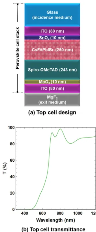
The perovskite top cell stack, given in Figure 1(a), has a planar structure and contains a semi-transparent cesium-formamidinium-based mixed halide (CsFAPbIBr) photoactive layer [15] with thickness of 250 nm and an optical bandgap of 1.68 eV. The chosen perovskite is known to be more stable than methylammonium-based compounds (MAPbI3-xBrx). Single-junction perovskite cell
stacks are usually prepared by spin-coating materials on glass substrates. Here, the top cell has an n-i-p configuration in which SnO2 and
Spiro-OMeTAD make up the electron and hole transport layers respectively. Contacts are formed by sputtered indium-doped tin oxide (ITO) on both sides. Typically, front-side reflection due to the planar structure and parasitic absorption in the contacting and carrier transport layers constitute optical losses in perovskite devices. Consequently, ultrathin non-active layers are desired for reducing parasitic absorption losses. However, the layers must be realistically thick for acceptable electrical performance in a working device. Therefore, at this stage where the electrical properties were not integrated into the model, the perovskite cell structure itself was not altered during GA-based optimization since the final solution from optical viewpoint would then always converge to maximum allowed perovskite thicknesses in combination with thinnest possible supporting layer values. Additionally, our top cell design incorporates an exit layer of MgF2 whose thickness
can be varied for improving transmittance (T) at IR wavelengths. The motivation for including a MgF2
exit layer comes from the results of a previous study where it was shown to have a similar impact on light in-coupling into the bottom cell as adapting the refractive index of an index matching medium (IMM) between the sub-cells [67]. It was then argued that the requirement for index matching could be relaxed by introducing a MgF2 exit layer
in the top cell design. However, if not optimized carefully, its inclusion could be counterproductive
Figure 1. (a) Schematic structure of the top cell, comprising perovskite cell layers and a MgF2 exit
medium. (b) Simulated transmitted spectrum (T) through the top cell into the bottom c-Si cell.
as a result of increased reflection at the ITO/MgF2
interface. Thus, for capturing longer wavelengths in the c-Si bottom cell, the MgF2 exit layer
thickness, the refractive index of the coupling medium, and the c-Si cell ARC thickness will all need to be concurrently adapted. The transmittance of the top cell, calculated using the transfer matrix method, is plotted in Figure 1(b).
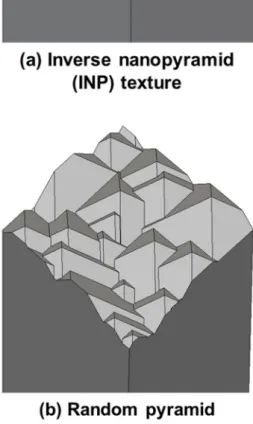
The c-Si bottom cell, in contrast, features pyramid textures of dimensions that are either comparable to or much larger than the wavelength
of the incoming light. Tilted top-view schematics of pyramid textures, considered in our study, are given in Figure 2.
Figure 2. Design parameters of (a) periodic inverse nanopyramid (INP) gratings as the front-surface texture in c-Si bottom cells were optimized using a genetic algorithm. (b) The standard random pyramid (RP) texture was adopted as the reference for drawing comparisons.
The INP pattern is a two-dimensional (2-D) diffraction grating of pitch comparable to the light wavelength scale, where neighboring pyramids are separated by flat regions (Figure 2(a)). The width of these flat regions is expressed as an area filling fraction, which is the ratio of the (non-flat) nanopatterned area to the total area. In view of minimizing reflection losses, realizing an area filling fraction of unity, i.e. having adjoining pyramids, is desirable but nonetheless challenging due to experimental constraints [44]. Therefore, a
realistic maximum area filling fraction of 0.8 [44] was assumed in the RCWA model for the INP texture. The industry standard random pyramid texture, produced by alkaline anisotropic etching, serves as the reference and consists of upright pyramids with base width size between 2 – 5 µm (Figure 2(b)). Moreover, different surface texture combinations were examined for both SHJ and SHJ-IBC bottom cell architectures when operating beneath a perovskite top cell (Figure 3).
III. MODELING APPROACH
The outlined optimization approach is aimed at maximizing net absorption in the CsFAPbIBr perovskite and c-Si photoactive layers of tandem devices. It uses spectrum-weighted absorption (ASW) as the figure of merit for quantifying total
absorption within the photoactive layers of sub-cells. Assuming an ideal carrier collection probability of one, ASW is indicative of the sum of
photogenerated currents that could potentially be drawn from individual sub-cells of a working 4-T tandem device. ASW is computed by the integral
provided in equation (I).
A = ∫ (Aper + A ) . φAM 1.5G λ2 λ1 . dλ ∫ φλλ2 AM 1.5G 1 . dλ (I)
In the expression above; Aper and ASi are the
wavelength-dependent absorption coefficients in perovskite and c-Si photoactive layers when the AM 1.5G solar spectrum is incident on a full 4-T tandem stack, φAM 1.5G represents the photon flux in the AM 1.5G solar spectrum and λ1 – λ2 is the
300 – 1200 nm wavelength interval. The expression therefore quantifies the fraction of incident photons that contribute to useful absorption in both sub-cells in a 4-T tandem structure.
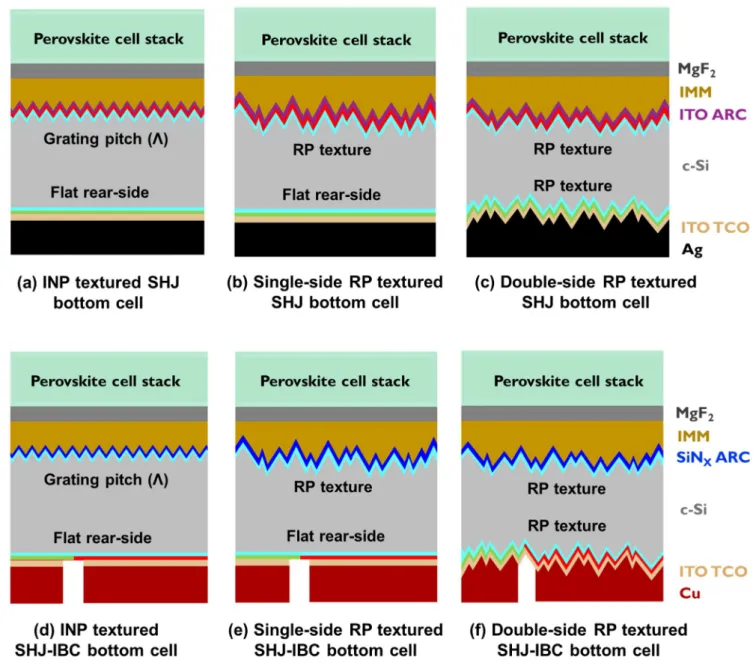
The suggested optimization procedure combines RCWA with a GA, described in Section IV, for modeling 4-T tandem devices with INP textured SHJ and SHJ-IBC bottom cells. For such tandem structures with a nanotextured bottom cell (Figures 3(a, d)), ASW was maximized by tweaking
certain design parameters which included thickness of the MgF2 exit layer (texit), refractive index of the
coupling medium (nIMM) that completely fills the
gap of 10 µm in between the sub-cells, antireflection coating (ARC) layer thickness for the bottom cell (tARC), grating pitch of the periodic INP
texture (Λ) and transparent conducting oxide (TCO) thickness on the rear-side of c-Si cell (tTCO).
Figure 3. Schematic structures of 4-T perovskite/c-Si tandem devices with either (a, d) inverse nanopyramid (INP) gratings or (b, c, e, f) the standard random pyramid (RP) texture present on the front-side of c-Si bottom cells. A heterojunction cell architecture was evaluated in this study in both (a – c) two-side contacted (SHJ) and (d – f) interdigitated and back-contacted (SHJ-IBC) configurations. For simplicity, different layers of perovskite cell stack are not shown.
The required RCWA simulations were performed using the open-source CAMFR tool [65]. As the
RCWA model assumes coherent wave
propagation, phase-elimination was applied for smoothing out the Fabry-Perot interference fringes which are otherwise absent at longer wavelengths for much thicker substrates [61]. Furthermore, deterministic ray tracing simulations with transfer matrix method (TMM) were performed in Sentaurus TCAD suite [66] for simulating the full 4-T tandem stack with single and double-sided RP textured bottom cells (Figures 3(b, c, e, f)). By defining TMM boundary condition at RP textured interfaces, interference effects in thin-film stacks are not neglected during each ray pass. An inherent limitation, however, of using the TMM boundary
condition with ray tracing is that the TMM lumps together the backward and forward wave components while assuming forward energy propagation. This simplification is necessary since the backward waves with decaying field amplitudes would then become forward waves with exponentially growing field amplitudes, leading to numerically unstable solutions. Therefore, it is critical to decouple the forward and backward components for calculating reflection and transmission coefficients. This is possible by either using TMM with the scattering matrices algorithm (S-matrix) or by performing mode sorting. The latter approach was adopted in our work in which the forward and backward wave components are distinguishable with the TMM, by considering
Poynting vectors for each propagating mode. The approach of combining ray tracing with the TMM boundary condition has been utilized before for simulating thin multilayer stacks in both single-junction [68,69] and 4-T tandem devices with textured interfaces [15]. In this way, we assess the optical boost at IR wavelengths by periodic nanoscale patterning of the bottom cell with respect to standard texturing. Here, optimal design parameter values were only extracted via the GA for INP textured bottom cells. The extracted values were then also assumed in the ray tracing model when simulating 4-T tandem devices with RP textured bottom cells for comparison purposes. These may not be their optimal values but nevertheless, our approach is generic and the scope of the study can be extended to include the coupling of a GA to a ray tracing model.
Optical models, based on RCWA and ray tracing with the TMM, were validated from measured reflectance spectra of INP and RP textured devices respectively at normal incidence (see Appendix). Relevant refractive indices (n, k) for optical simulations were obtained from spectroscopic ellipsometry measurements.
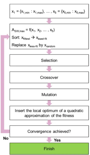
IV. GENETIC ALGORITHM DESCRIPTION A GA enables to identify the combination of variables that will maximize a given objective function (fitness) without having to sweep all their possible combinations [56,57]. It emulates natural selection by performing biological operations of selection, crossover and mutation on a random population of variables for successive generations until a specified goal is realized. Our GA flow, which was described with details in previous works [58-60], is given in Figure 4.
Five interdependent cell design parameters (x1 = nIMM, x2 = texit, x3 = tARC, x4 = Λ, and x5 = tTCO)
were considered in the optimization of 4-T tandem structures. A search range and a desired resolution, typically 0.1 for x1 and 1 nm for x2 – x4, are defined
at the beginning of the optimization problem for each involved variable. These specifications lead to an appropriate binary encoding of these variables. A population of 50 individuals is then considered, where an individual corresponds to a possible solution ⃗ = (x1, x2, x3, x4, x5) of the optimization
problem and is represented by a binary digit sequence or DNA. The objective, in the case described in this work, is to establish a solution (optimal values of x1 – x5 within the search range)
that will maximize ASW in the simulated tandem
structures. Starting from a random population of
individuals (random values of x1 – x5 within the
search range), the population is sorted from the fittest (giving the highest ASW) to the least-fit
individual after performing RCWA simulations for evaluating the fitness f( ⃗) of each individual. The least-fit individuals (up to 10% of the population) are excluded from further evaluations and replaced by an equal number of random individuals. The fitter individuals of the original population are selected by a rank-based roulette wheel selection for performing the crossover and mutation operations on their binary digit sequences or DNA to produce individuals (children) for the subsequent generation. The crossover operation here refers to exchanging a part of the binary digit sequence of two selected individuals (parents), with a probability (rate of crossover) of 70%. The mutation operation after crossover simply randomly reverses some binary digits in a child’s DNA.
Figure 4. Genetic algorithm (GA) flow for mimicking natural selection procedure. The optimization is aimed at maximizing spectrum-weighted absorption (ASW) in
were carried out with a population size npop of 50
individuals, a crossover rate of 70% and a mutation rate of 0.95/nbits, where nbits is the number of bits required for
coding the considered variables (nbits ~50 for 5
variables). The number of random individuals injected at each generation is 0.1 × npop × (1 − p), where p = |s −
0.5|/0.5 and s is the fraction of bits in the population whose value is identical to the best individual. The number of generations required for an optimization is typically between 25 and 40.
A bit mutation probability of 0.95/(number of binary digits in a DNA) was assumed in our GA flow. Afterwards, a local optimization procedure is conducted on the data collected by the algorithm. This local optimization procedure essentially makes use of a quadratic approximation of the fitness around the best-known individual for substituting a random individual in the population by an optimal individual determined from the approximation. We used a quadratic approximation of the fitness since establishing this approximation and its optimum is tractable when less than 20 variables are involved in an optimization problem [59,60]. Finally, the individuals generated for the next generation (children) are subjected to fitness evaluation by running RCWA simulations and sorted according to their fitness. Elitism is implemented in order to ensure that the best solution is not lost when going from one generation to the next. Elitism implies that if the best individual of the new generation is not as good as for the previous generation, the best individual of the previous generation will be retained for replacing a randomly chosen individual of the new generation. This natural selection cycle is repeated for multiple generations until the results converge to an optimal solution. Thus, by implementing the computationally intense RCWA simulations for a reasonably sized population of individuals in every fitness evaluation cycle, we were able to determine the optimal x1 – x5 parameter values that lead to the
highest ASW in the investigated tandem device
structures.
V. RESULTS AND DISCUSSION
We first present the optimization results for the INP textured bottom cells and then compare them with the performance of RP textured counterparts.
A. Genetic algorithm results for inverse nanopyramid textured devices
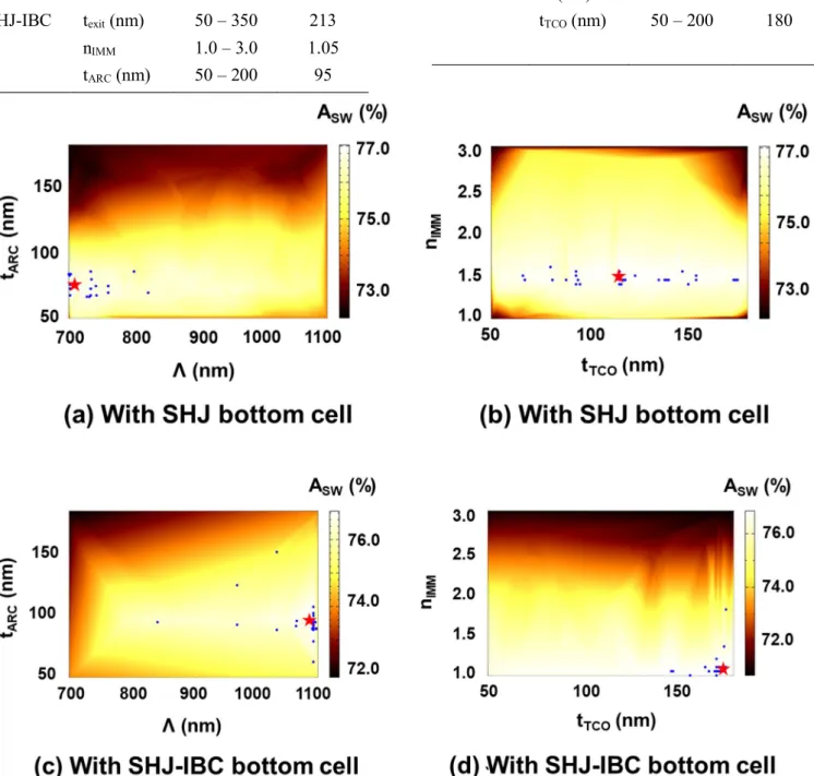
Fitness evaluation maps of the GA-based optimization for c-Si bottom cells are shown in
Figures 5(a, b) for SHJ and in Figures 5(c, d) for SHJ-IBC structures respectively and the outcome is also summarized in Table I along with the considered range of values for each design parameter. These maps illustrate differences between optimal device parameters of both cell structures, when employed as bottom cells. More importantly, they give an idea of the extent and direction of sensitivity of the chosen figure of merit (ASW) on a given device parameter.
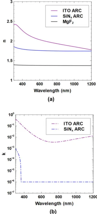
Comparing ARC layer thicknesses in best cases, we observe that a thinner ITO of 72 nm on the front is favored in the SHJ structure (Figure 5(a)) as opposed to a slightly thicker silicon nitride (SiNx) layer of 95 nm in the IBC structure (Figure
5(c)). This finding is attributed to the different complex refractive indices of ITO and SiNx films,
provided in Figure 6, influencing light in-coupling at the IMM/ARC interface as well as parasitic absorption losses in these films. The fitness maps also show that adapting a bottom cell’s ARC thickness, regardless of its cell architecture, is much more critical than the other optical design parameters for 4-T tandem application. Thus, the ARC thickness must be tuned accordingly for capturing the transmitted wavelengths into the c-Si bottom cell.
TABLE I
SUMMARY OF OPTIMAL DESIGN PARAMETERS THAT WERE EXTRACTED BY COMBINING RCWA WITH A GENETIC ALGORITHM. THESE PARAMETERS INCLUDE: MgF2 EXIT LAYER
THICKNESS (texit), REFRACTIVE INDEX OF THE
COUPLING MEDIUM (nIMM), BOTTOM CELL ARC
THICKNESS (tARC), GRATING PERIOD OF THE
FRONT-SIDE TEXTURE (Λ), AND THE TCO THICKNESS ON THE REAR-SIDE OF BOTTOM CELL (tTCO). THE OPTIMZATION WAS
PERFORMED FOR INVERSE NANOPYRAMID TEXTURED SHJ AND SHJ-IBC BOTTOM CELLS BENEATH A PEROVSKITE TOP CELL IN 4-T TANDEM CONFIGURATION. Bottom cell design Parameter Search range Optimal value SHJ texit (nm) nIMM tARC (nm) Λ (nm) tTCO (nm) 50 – 350 1.0 – 3.0 50 – 200 700 – 1100 50 – 200 213 1.5 72 710 114
SHJ-IBC texit (nm) 50 – 350 213 nIMM tARC (nm) 1.0 – 3.0 50 – 200 1.05 95 Λ (nm) tTCO (nm) 700 – 1100 50 – 200 1090 180
Figure 5. 2-D fitness maps for inverse nanopyramid textured (a, b) SHJ and (c, d) SHJ-IBC bottom cells, operating below a perovskite top cell in 4-T tandem configuration. Optical models based on RCWA were coupled with the genetic algorithm for determining optimal values of the antireflection coating layer thickness (tARC), the grating period (Λ),
refractive index of the coupling medium between sub-cells (nIMM), rear-side transparent conducting oxide layer thickness
(tTCO) and MgF2 exit layer thickness (texit). The maps represent the fittest solutions from successive generations (blue
dots) that converge to the optimal solution (red star). The spectrum-weighted absorption (ASW) quantifies the useful
absorption within the photoactive layers.
In addition to ARC layer thickness, light in-coupling into the bottom c-Si cell should be influenced by the grating period of the nanopyramid surface texture and the refractive index of the coupling medium. The grating pitch of the INP texture could also be used as a control parameter for enhancing absorption in c-Si sub-cells at desired wavelengths. 2-D fitness maps in Figures 5(a) and 5(c) reveal optimal grating periods of 710 nm and 1090 nm respectively for SHJ and SHJ-IBC device structures, suggesting different
intended wavelength ranges. Optimal grating pitch values are also consistent with ARC layer thicknesses and suggest that while the IR wavelengths are being targeted by an INP textured SHJ-IBC bottom cell, the intermediate wavelengths appear to be more relevant for the SHJ case. To explain this observed opposite trend in optimal grating periods, parasitic losses were then extracted for both tandem structures. The results, given in Figure 7, show significant absorption in the ITO ARC layer compared to SiNx in the 1000 –
current density loss of 0.57 mA/cm2 in the SHJ
bottom cell structure in contrast to only 0.17 mA/cm2 for the SHJ-IBC structure. Accordingly, in
consideration of parasitic absorption losses in ITO at IR wavelengths, the optimal grating period gets smaller for efficiently confining intermediate wavelengths within the substrate of a SHJ device. On the other hand, in a SHJ-IBC device, a larger pitch aids in trapping IR wavelengths where parasitic losses in SiNx are marginal and the
incident photon flux is substantial. However, it is noteworthy that a relatively wide window is available for the choice of the grating period in both cell structures. Spectrum-weighted absorption only varies slightly from 76.1% to 76.5% for the SHJ bottom cell structure as the grating pitch is reduced from 900 nm to 710 nm. In the case of the SHJ-IBC cell structure, it rises from 75.9% to 76.4% upon increasing the pitch from 950 nm to 1090 nm. This small variation in the spectrum-weighted absorption as function of the grating pitch lies within the ±0.6% numerical error of RCWA, arising from Fabry-Perot interference fringes at wavelengths above 1000 nm under the assumption of coherent wave propagation, and can therefore be neglected.
Besides adapting the grating period and the ARC layer thickness, we find that inclusion of an optical coupling medium with nIMM ~1.5 could
facilitate transmission by offering a graded index effect at the IMM/ITO interface in a 4-T perovskite/SHJ tandem device (Figure 5(b)). Nevertheless, the need for introducing an index matching layer between sub-cells does not arise in a 4-T perovskite/SHJ-IBC tandem structure since a SiNx ARC layer has a lower refractive index than
ITO in the entire wavelength range (Figure 6(a)). The result in Figure 5(d) implies that an air gap already provides favorable optical coupling to a SHJ-IBC bottom cell, when a MgF2 layer of ~213
nm thickness is present as the exit medium in top cell design. This thickness of ~213 nm for MgF2
exit layer was found to be independent of the bottom cell design since its role is only to enhance IR transmission through the top cell during the first light pass.
Lastly, the thickness of the rear-side ITO is the least critical parameter for both bottom cell structures. Provided that the rear-side transparent conducting oxide layer is sufficiently thick (> 100 nm), it can efficiently serve as an optical spacer for suppressing the excitation of surface plasmons [62] by absorbing and reflecting longer wavelength photons. Since silver (Ag) offers superior reflectivity and lower parasitic absorption losses as
the rear-side metal contact than copper (Cu), the required ITO thickness on the rear-side of a SHJ device with Ag (114 nm) was also found to be relatively thinner than for a SHJ-IBC device with Cu (180 nm).
Figure 6. Complex refractive indices of ITO and SiNX
antireflection coating layers that are employed in SHJ and SHJ-IBC bottom cells respectively. (a) SiNX has a
lower refractive index (n) than ITO over the entire spectrum. The refractive index of the MgF2 exit medium
is also indicated for reference. (b) Extinction coefficient (k) values are much higher for ITO and could result in significant parasitic absorption losses in SHJ devices.
Figure 7. Parasitic absorption losses were calculated in the 300 – 1200 nm wavelength interval for mechanically stacked and optically optimized (a) perovskite/SHJ and (b) perovskite/SHJ-IBC tandem devices, featuring inverse nanopyramid gratings on the front-side of the c-Si bottom cells.
B. Comparison between inverse nanopyramid and random pyramid textured devices
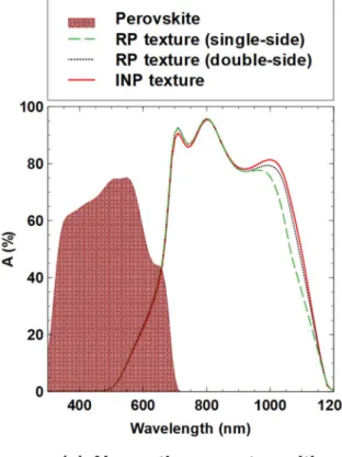
In order to examine potential IR absorption enhancement by substituting standard random pyramid textures by wavelength scale pyramid gratings for light management in tandem devices, deterministic ray-tracing simulations were carried out for 4-T tandem structures with single and double-sided random pyramid textured bottom cells, shown schematically in Figures 3(b, c, e, f). Since the scope of the study was limited to coupling RCWA-based optical models to GA, optimal parameter values for INP textured bottom cells in Table I were also utilized in ray tracing simulations. Although this approach does not lead to an accurate comparison between the two texture types, it nevertheless allows to identify possible optical gain sources by introducing single-side nanopyramid gratings in place of the standard micron-scale pyramids as light management structures in 4-T tandem devices.
Optical boost at IR wavelengths (> 900 nm) by nanopatterning is apparent from c-Si absorption curves in Figure 8. For the SHJ case (Figure 8(a)), spectrum-weighted absorption in the tandem stack increases from 74.9% to 76.5% when the random pyramid texture on the front-side of bottom cell is replaced by nanopyramid gratings to provide a current density gain in the c-Si cell of 0.73 mA/cm2. The improvement can be assumed to
originate from the excitation of higher order modes [63] and the wave-optical nature of light-trapping in a nanophotonic structure. As the incoming light is primarily absorbed in the perovskite absorber during the first pass, the front-surface texture of the bottom cell does not impact photogeneration in the top cell. This is mainly because the reflected IR wavelengths at the IMM/ARC interface are optically transparent to the wider bandgap perovskite and are therefore only parasitically absorbed in the supporting layers of the top cell.
However, the absorption curves in Figure 8(a) also show that this boost becomes negligible if random pyramids are textured on both cell sides. Thus, double-side random pyramid textured devices with spectrum-weighted absorption of 76.4% are optically equivalent to their single-side nanopatterned counterparts or even better, when considering that the dielectric stack may not be optimum for this texture type. This is because a textured rear-side in combination with Ag back reflector in the SHJ structure, scatters the in-coupled light more effectively at higher angles within the substrate than a flat-rear counterpart and
Figure 8. Absorption in perovskite and c-Si substrates for random pyramid (RP) and inverse nanopyramid (INP) textured (a) SHJ and (b) SHJ-IBC bottom cells under a perovskite top cell. Single and double-sided random pyramid textured devices, shown in Figures 3(b, c, e, f), were taken as reference for benchmarking the absorption enhancement at longer wavelengths by nanopatterning.
is therefore able to achieve comparable IR absorption as the front-side INP grating texture. In contrast, when a SHJ-IBC bottom cell is deployed, increased transmission losses through the electrical isolation gap between interdigitated Cu electrodes lead to reduced IR absorption with double-side random pyramid texture and a spectrum-weighted absorption value of 75.4% is achieved (Figure 8(b)). On the contrary, front-surface pyramid textures with a flat rear-side yield higher absorption at longer wavelengths by cutting down the transmitted fraction of the in-coupled light. Moreover, for INP textured SHJ-IBC cells, Figure 8(b) shows a minor drop in the absorption at intermediate wavelengths (620 – 750 nm) which is a consequence of implementing gratings that were fine-tuned for targeting wavelengths beyond 1000 nm. Nonetheless, the loss is negligible as shown by the similar spectrum-weighted absorption of single-sided RP (77.0%) and INP (76.4%) textures. The findings reported in Figure 8 seem to indicate that replacing standard random pyramid texture by nanopyramid gratings would not result in a significant absorption gain at IR wavelengths. However, it needs to be emphasized here that the
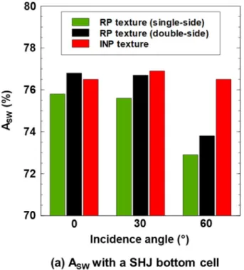
simulations above were performed for
perpendicularly incident illumination and therefore do not account for the sun’s movement along the horizon. This is especially important for 4-T tandems since these do not need current matching and are therefore going to be used for applications where such non-perpendicular illumination will be abundant. We evaluated the impact of variation in the incidence angle on the spectrum-weighted absorption of the investigated tandem device structures by assuming an unchanged azimuthal angle of 45° and reducing the AM 1.5G spectral power density by cosine of the incidence angle. The results of incidence angle dependence in Figure 9 point to the fundamental difference in the light-trapping mechanism of micron and nanoscale textures. Since the incoming light interacts at the interface of a random pyramid textured surface in the geometrical-optics regime, escape losses are inevitable for certain incidence angles as the in-coupled rays cannot be trapped by means of total internal reflection in the absorber. With nanopyramid gratings present as the surface texture, the interaction occurs instead in the wave-optics regime and thereby eliminates angular dependence by transmitting the incident light into modes. A carefully designed grating is thus able to confine the incoming light to diffraction modes that are outside the escape loss angular range [64]. As a
Figure 9. Spectrum-weighted absorption (ASW) as
function of the incidence angle for optimal (a) SHJ and (b) SHJ-IBC bottom cells, operating beneath the top cell given in Figure 2(a). An incidence angle of 0° refers to perpendicularly incoming light. The azimuthal angle was assigned a constant value of 45° while the incidence angle was varied for different texturing schemes.
result, we observe in Figure 9 that the spectrum-weighted absorption falls less drastically with increasing angle of incidence for an INP textured sub-cell and could potentially lead to a higher annual energy yield. Hence, it can be deduced from Figure 9 that the angular robustness presents a major motivation for replacing standard random pyramid textured bottom cells by their INP
patterned analogues in 4-T perovskite/c-Si tandem device structures.
VI. CONCLUSION
It was demonstrated that optical models could be coupled with a genetic algorithm for optimizing five interdependent design parameters of tandem solar devices at once. In theory, the presented approach is not limited by the number of interdependent design parameters. Specifically, in this case, the optimization was carried out for
inverse nanopyramid textured silicon
heterojunction devices that operate as bottom cells beneath a wider bandgap perovskite top cell. Coupling rigorous coupled-wave analysis with a genetic algorithm enabled us to reduce the required
number of computationally expensive
electromagnetic wave simulations for extracting optimal values of a given set of variables. While keeping the thicknesses of top cell layers unchanged, the objective herein was to obtain bottom cell design parameters for maximizing total absorption in the perovskite and crystalline-silicon substrates. The study was conducted for both two-side contacted (SHJ) and interdigitated-back-contacted (SHJ-IBC) silicon heterojunction devices, incorporating inverse nanopyramid gratings as the front-surface texture. In this regard, the GA-based optimization enabled to identify the most sensitive design parameters when switching to nanopyramid diffraction gratings for light management in tandem devices. It was found for both investigated cell architectures that adapting the bottom cell antireflection coating (ARC) layer thickness was more critical than the grating period of the nanotexture. Likewise, the need for an optical coupling medium between the sub-cells is subject to the refractive index of the ARC layer. Benchmarking the optical performance of inverse nanopyramid textured silicon heterojunction bottom cells with their random pyramid textured counterparts, we found that only marginal improvement in infrared absorption was achieved by integrating front-side gratings. Nevertheless, the improvement by nanopatterning the bottom cell becomes more significant when considering non-perpendicular incident light in view of the annual energy yield.
ACKNOWLEDGEMENT
The authors are grateful to the partners of imec’s industrial affiliation program for Silicon PV (IIAP-PV). The work in this paper was partially funded by the Kuwait Foundation for the Advancement of Sciences under project number CN18-15EE-01.
Imec is a partner in EnergyVille
(www.energyville.be), a collaboration between the Flemish research partners KU Leuven, VITO, imec and Universiteit Hasselt in the field of sustainable energy and intelligent energy systems. Alexandre Mayer is funded by the Fund for Scientific Research (F.R.S.-FNRS) of Belgium. This research used resources of the “Plateforme Technologique de Calcul Intensif (PTCI)” located at the University of Namur, Belgium, which is supported by the FNRS-FRFC, the Walloon Region, and the University of Namur (Conventions No. 2.5020.11, GEQ U.G006.15, 1610468 and RW/GEQ2016). The PTCI is member of the “Consortium des Equipements de Calcul Intensif (CECI)” (http://www.ceci-hpc.be).
APPENDIX
VALIDATED RCWA AND RAY TRACING BASED OPTICAL MODELS FOR INVERSE NANOPYRAMID AND RANDOM PYRAMID
TEXTURED SILICON HETEROJUNCTION SOLAR CELLS RESPECTIVELY
REFERENCES
[1] R. Fu, D. J. Feldman, and R. M. Margolis. “U.S. Solar Photovoltaic System Cost
Benchmark: Q1 2018,” National
Renewable Energy Laboratory,
NREL/TP-6A20-72399, 2018.
[2] K. Yamamoto, K. Yoshikawa, K. Uzu, and D. Adachi. “High-efficiency heterojunction crystalline Si solar cells,” Japanese Journal
of Applied Physics, vol. 57, 08RB20, 2018.
[3] K. Yoshikawa, H. Kawasaki, W. Yoshida, T. Irie, K. Konishi, K. Nakano, T. Uto, D. Adachi, M. Kanematsu, H. Uzu, and K. Yamamoto, “Silicon heterojunction solar cell with interdigitated back contacts for a photoconversion efficiency over 26%,”
Nature Energy, vol. 2, no. 5, 2017.
[4] F. Haase, C. Hollemann, S. Schäfer, A. Merkle, M. Rienäcker, J. Krügener, R. Brendel, and R. Peibst, “Laser contact openings for local poly-Si-metal contacts enabling 26.1%-efficient POLO-IBC solar cells,” Solar Energy Materials and Solar
Cells, vol. 186, pp. 184–193, 2018.
[5] T. Leijtens, K. A. Bush, R. Prasanna, and M. D. Mcgehee, “Opportunities and challenges for tandem solar cells using metal halide perovskite semiconductors,”
Nature Energy, vol. 3, no. 10, pp. 828–838,
2018.
[6] J. P. Mailoa, M. Lee, I. M. Peters, T. Buonassisi, A. Panchula, and D. N. Weiss, “Energy-yield prediction for II–VI-based thin-film tandem solar cells,” Energy &
Environmental Science, vol. 9, no. 8, pp.
2644–2653, 2016.
[7] M. T. Hörantner and H. J. Snaith, “Predicting and optimising the energy yield of perovskite-on-silicon tandem solar cells under real world conditions,” Energy &
Environmental Science, vol. 10, no. 9, pp.
1983–1993, 2017.
[8] F. Sahli, J. Werner, B. A. Kamino, M. Bräuninger, R. Monnard, B. Paviet-Salomon, L. Barraud, L. Ding, J. J. D. Leon, D. Sacchetto, G. Cattaneo, M. Despeisse, M. Boccard, S. Nicolay, Q. Jeangros, B. Niesen, and C. Ballif, “Fully textured monolithic perovskite/silicon tandem solar cells with 25.2% power conversion efficiency,” Nature Materials, vol. 17, no. 9, pp. 820–826, 2018.
[9] J. Werner, B. Niesen, and C. Ballif, “Perovskite/Silicon Tandem Solar Cells:
Marriage of Convenience or True Love Story? - An Overview,” Advanced
Materials Interfaces, vol. 5, no. 1, p.
1700731, 2017.
[10] T. Leijtens, K. A. Bush, R. Prasanna, and M. D. Mcgehee, “Opportunities and challenges for tandem solar cells using metal halide perovskite semiconductors,”
Nature Energy, vol. 3, no. 10, pp. 828–838,
2018.
[11] G. E. Eperon, M. T. Hörantner, and H. J. Snaith, “Metal halide perovskite tandem and multiple-junction photovoltaics,”
Nature Reviews Chemistry, vol. 1, no. 12,
2017.
[12] F. Fu, T. Feurer, T. P. Weiss, S. Pisoni, E. Avancini, C. Andres, S. Buecheler, and A. N. Tiwari, “High-efficiency inverted semi-transparent planar perovskite solar cells in substrate configuration,” Nature Energy, vol. 2, no. 1, 2016.
[13] T. Duong, Y. Wu, H. Shen, J. Peng, X. Fu, D. Jacobs, E.-C. Wang, T. C. Kho, K. C. Fong, M. Stocks, E. Franklin, A. Blakers, N. Zin, K. Mcintosh, W. Li, Y.-B. Cheng, T. P. White, K. Weber, and K. Catchpole, “Rubidium Multication Perovskite with Optimized Bandgap for Perovskite-Silicon Tandem with over 26% Efficiency,”
Advanced Energy Materials, vol. 7, no. 14,
p. 1700228, 2017.
[14] J. Werner, L. Barraud, A. Walter, M. Bräuninger, F. Sahli, D. Sacchetto, N. Tétreault, B. Paviet-Salomon, S.-J. Moon, C. Allebé, M. Despeisse, S. Nicolay, S. D. Wolf, B. Niesen, and C. Ballif, “Efficient Near-Infrared-Transparent Perovskite Solar Cells Enabling Direct Comparison of
4-Terminal and Monolithic
Perovskite/Silicon Tandem Cells,” ACS
Energy Letters, vol. 1, no. 2, pp. 474–480,
2016.
[15] M. Jaysankar, M. Filipič, B. Zielinski, R. Schmager, W. Song, W. Qiu, U. W. Paetzold, T. Aernouts, M. Debucquoy, R. Gehlhaar, and J. Poortmans, “Perovskite– silicon tandem solar modules with optimised light harvesting,” Energy &
Environmental Science, vol. 11, no. 6, pp.
1489–1498, 2018.
[16] U. W. Paetzold, M. Jaysankar, R. Gehlhaar, E. Ahlswede, S. Paetel, W. Qiu, J. Bastos, L. Rakocevic, B. S. Richards, T. Aernouts, M. Powalla, and J. Poortmans, “Scalable perovskite/CIGS thin-film solar module
with power conversion efficiency of 17.8%,” Journal of Materials Chemistry A, vol. 5, no. 20, pp. 9897–9906, 2017.
[17] K. A. Bush, A. F. Palmstrom, Z. J. Yu, M. Boccard, R. Cheacharoen, J. P. Mailoa, D. P. Mcmeekin, R. L. Z. Hoye, C. D. Bailie, T. Leijtens, I. M. Peters, M. C. Minichetti, N. Rolston, R. Prasanna, S. Sofia, D. Harwood, W. Ma, F. Moghadam, H. J. Snaith, T. Buonassisi, Z. C. Holman, S. F. Bent, and M. D. Mcgehee, “23.6%-efficient monolithic perovskite/silicon tandem solar cells with improved stability,” Nature
Energy, vol. 2, no. 4, 2017.
[18] S. D. Wolf, J. Holovsky, S.-J. Moon, P. Löper, B. Niesen, M. Ledinsky, F.-J. Haug, J.-H. Yum, and C. Ballif, “Organometallic Halide Perovskites: Sharp Optical Absorption Edge and Its Relation to Photovoltaic Performance,” The Journal of
Physical Chemistry Letters, vol. 5, no. 6,
pp. 1035–1039, 2014.
[19] G. E. Eperon, T. Leijtens, K. A. Bush, R. Prasanna, T. Green, J. T.-W. Wang, D. P. McMeekin, G. Volonakis, R. L. Milot, R. May, A. Palmstrom, D. J. Slotcavage, R. A. Belisle, J. B. Patel, E. S. Parrott, R. J. Sutton, W. Ma, F. Moghadam, B. Conings, A. Babayigit, H.-G. Boyen, S. Bent, F. Giustino, L. M. Herz, M. B. Johnston, M. D. McGehee, and H. J. Snaith. Perovskite-Perovskite Tandem Photovoltaics with Optimized Bandgaps. Science, vol. 354, pp. 861–865, 2016.
[20] G. E. Eperon, S. D. Stranks, C. Menelaou, M. B. Johnston, L. M. Herz, and H. J. Snaith, “Formamidinium lead trihalide: a broadly tunable perovskite for efficient planar heterojunction solar cells,” Energy
& Environmental Science, vol. 7, no. 3, p.
982, 2014.
[21] E. L. Unger, L. Kegelmann, K. Suchan, D. Sörell, L. Korte, and S. Albrecht, “Correction: Roadmap and roadblocks for the band gap tunability of metal halide perovskites,” Journal of Materials Chemistry A, vol. 5, no. 30, pp. 15983–
15983, 2017.
[22] S. Y. Herasimenka, W. J. Dauksher, and S. G. Bowden, “>750 mV open circuit voltage measured on 50 μm thick silicon heterojunction solar cell,” Applied Physics
Letters, vol. 103, no. 5, p. 053511, 2013.
[23] M. Taguchi, A. Yano, S. Tohoda, K. Matsuyama, Y. Nakamura, T. Nishiwaki,
K. Fujita, and E. Maruyama, “24.7% Record Efficiency HIT Solar Cell on Thin Silicon Wafer,” IEEE Journal of
Photovoltaics, vol. 4, no. 1, pp. 96–99,
2014.
[24] A. Fell, K. R. McIntosh, P. P. Altermatt, G. J. M. Janssen, R. Stangl, A. Ho-Baillie, H. Steinkemper, J. Greulich, M. Müller, B. Min, K. C. Fong, M. Hermle, I. G. Romijn, and M. D. Abbot, “Input Parameters for the Simulation of Silicon Solar Cells in 2014,”
IEEE Journal of Photovoltaics, vol. 5, no.
4, pp. 1250–1263, 2015.
[25] P. Sheng, A. N. Bloch, and R. S. Stepleman,
“Wavelength‐selective absorption
enhancement in thin‐film solar cells,”
Applied Physics Letters, vol. 43, no. 6, pp.
579–581, 1983.
[26] C. Heine and R. H. Morf, “Submicrometer gratings for solar energy applications,”
Applied Optics, vol. 34, no. 14, p. 2476,
1995.
[27] Z. Yu, A. Raman, and S. Fan, “Fundamental limit of light trapping in grating structures,” Optics Express, vol. 18, no. S3, 2010.
[28] M. Peters, M. Rüdiger, H. Hauser, M. Hermle, and B. Bläsi, “Diffractive gratings for crystalline silicon solar cells-optimum parameters and loss mechanisms,”
Progress in Photovoltaics: Research and Applications, vol. 20, no. 7, pp. 862–873,
2011.
[29] R. Cariou, J. Benick, F. Feldmann, O. Höhn, H. Hauser, P. Beutel, N. Razek, M. Wimplinger, B. Bläsi, D. Lackner, M. Hermle, G. Siefer, S. W. Glunz, A. W. Bett, and F. Dimroth, “III–V-on-silicon solar cells reaching 33% photoconversion efficiency in two-terminal configuration,”
Nature Energy, vol. 3, no. 6, pp. 529–529,
2018.
[30] V. Depauw, X. Meng, O. E. Daif, G. Gomard, L. Lalouat, E. Drouard, C. Trompoukis, A. Fave, C. Seassal, and I. Gordon, “Micrometer-Thin Crystalline-Silicon Solar Cells Integrating Numerically Optimized 2-D Photonic Crystals,” IEEE
Journal of Photovoltaics, vol. 4, no. 1, pp.
215–223, 2013.
[31] H. Savin, P. Repo, G. V. Gastrow, P. Ortega, E. Calle, M. Garín, and R. Alcubilla, “Black silicon solar cells with interdigitated back-contacts achieve 22.1%
efficiency,” Nature Nanotechnology, vol. 10, no. 7, pp. 624–628, 2015.
[32] A. Ingenito, O. Isabella, and M. Zeman,
“Nano-cones on micro-pyramids:
modulated surface textures for maximal spectral response and high-efficiency solar cells,” Progress in Photovoltaics: Research
and Applications, vol. 23, no. 11, pp. 1649–
1659, 2015.
[33] P. Spinelli, M. Verschuuren, and A. Polman, “Broadband omnidirectional
antireflection coating based on
subwavelength surface Mie resonators,”
Nature Communications, vol. 3, no. 1,
2012.
[34] P. Spinelli, B. K. Newman, and A. Polman, “Photovoltaics: Light-Trapping in Crystalline Silicon and Thin-Film Solar Cells by Nanostructured Optical Coatings,”
Nanotechnology for Energy Sustainability,
pp. 163–180, 2017.
[35] A. Razzaq, V. Depauw, H. S.
Radhakrishnan, J. Cho, I. Gordon, J. Szlufcik, Y. Abdulraheem, and J.
Poortmans, “Infrared Absorption
Enhancement Using Periodic Inverse Nanopyramids in Crystalline-Silicon Bottom Cells for Application in Tandem Devices,” IEEE Journal of Photovoltaics, vol. 10, no. 3, pp. 740–748, 2020.
[36] C. Trompoukis, O. E. Daif, V. Depauw, I. Gordon, and J. Poortmans, “Photonic assisted light trapping integrated in ultrathin crystalline silicon solar cells by nanoimprint lithography,” Applied Physics
Letters, vol. 101, no. 10, p. 103901, 2012.
[37] C. Trompoukis, I. Abdo, R. Cariou, I. Cosme, W. Chen, O. Deparis, A. Dmitriev, E. Drouard, M. Foldyna, E. G.- Caurel, I. Gordon, B. Heidari, A. Herman, L. Lalouat, K.-D. Lee, J. Liu, K. Lodewijks, F. Mandorlo, I. Massiot, A. Mayer, V. Mijkovic, J. Muller, R. Orobtchouk, G. Poulain, P. Prodhomme, P. R. I. Cabarrocas, C. Seassal, J. Poortmans, R. Mertens, O. E. Daif, and V. Depauw, “Photonic nanostructures for advanced light trapping in thin crystalline silicon solar cells,” physica status solidi (a), vol. 212, no. 1, pp. 140–155, 2014.
[38] M. S. Branham, W.-C. Hsu, S. Yerci, J. Loomis, S. V. Boriskina, B. R. Hoard, S. E. Han, and G. Chen, “Silicon Solar Cells: 15.7% Efficient 10-μm-Thick Crystalline Silicon Solar Cells Using Periodic
Nanostructures (Adv. Mater. 13/2015),”
Advanced Materials, vol. 27, no. 13, pp.
2268–2268, 2015.
[39] A. Bozzola, M. Liscidini, and L. C. Andreani, “Photonic light-trapping versus Lambertian limits in thin film silicon solar cells with 1D and 2D periodic patterns,”
Optics Express, vol. 20, no. S2, 2012.
[40] J. Oh, H.-C. Yuan, and H. M. Branz, “An 18.2%-efficient black-silicon solar cell achieved through control of carrier recombination in nanostructures,” Nature
Nanotechnology, vol. 7, no. 11, pp. 743–
748, 2012.
[41] P. Repo, A. Haarahiltunen, L. Sainiemi, M. Yli-Koski, H. Talvitie, M. C. Schubert, and H. Savin, “Effective Passivation of Black Silicon Surfaces by Atomic Layer
Deposition,” IEEE Journal of
Photovoltaics, vol. 3, no. 1, pp. 90–94,
2013.
[42] C. Trompoukis, O. E. Daif, P. P. Sharma, H. S. Radhakrishnan, M. Debucquoy, V. Depauw, K. V. Nieuwenhuysen, I. Gordon, R. Mertens, and J. Poortmans, “Passivation of photonic nanostructures for crystalline silicon solar cells,” Progress in Photovoltaics: Research and Applications,
vol. 23, no. 6, pp. 734–742, 2014.
[43] C. Trompoukis, A. Stesmans, E. Simoen, V. Depauw, O. E. Daif, K. Lee, I. Gordon, R. Mertens, and J. Poortmans, “Photonic nanostructures for advanced light trapping in silicon solar cells: the impact of etching on the material electronic quality,” physica
status solidi (RRL) - Rapid Research Letters, vol. 10, no. 2, pp. 158–163, 2015.
[44] A. Razzaq, V. Depauw, J. Cho, H. S. Radhakrishnan, I. Gordon, J. Szlufcik, Y. Abdulraheem, and J. Poortmans, “Periodic inverse nanopyramid gratings for light management in silicon heterojunction devices and comparison with random pyramid texturing,” Solar Energy Materials
and Solar Cells, vol. 206, p. 110263, 2020.
[45] F. Sahli, B. A. Kamino, J. Werner, M. Bräuninger, B. Paviet-Salomon, L. Barraud, R. Monnard, J. P. Seif, A. Tomasi, Q. Jeangros, A. Hessler-Wyser, S. D. Wolf, M. Despeisse, S. Nicolay, B. Niesen, and C. Ballif, “Improved Optics in Monolithic Perovskite/Silicon Tandem Solar Cells with a Nanocrystalline Silicon Recombination Junction,” Advanced Energy Materials, vol. 8, no. 6, p. 1701609, 2017.
[46] J. Werner, L. Barraud, A. Walter, M. Bräuninger, F. Sahli, D. Sacchetto, N. Tétreault, B. Paviet-Salomon, S.-J. Moon, C. Allebé, M. Despeisse, S. Nicolay, S. D. Wolf, B. Niesen, and C. Ballif, “Efficient Near-Infrared-Transparent Perovskite Solar Cells Enabling Direct Comparison of
4-Terminal and Monolithic
Perovskite/Silicon Tandem Cells,” ACS
Energy Letters, vol. 1, no. 2, pp. 474–480,
2016.
[47] D. P. Mcmeekin, G. Sadoughi, W. Rehman, G. E. Eperon, M. Saliba, M. T. Horantner, A. Haghighirad, N. Sakai, L. Korte, B. Rech, M. B. Johnston, L. M. Herz, and H. J. Snaith, “A cation lead mixed-halide perovskite absorber for tandem solar cells,” Science, vol. 351, no. 6269, pp. 151– 155, 2016.
[48] J. Peng, T. Duong, X. Zhou, H. Shen, Y. Wu, H. K. Mulmudi, Y. Wan, D. Zhong, J. Li, T. Tsuzuki, K. J. Weber, K. R. Catchpole, and T. P. White, “Efficient Indium-Doped TiOx Electron Transport Layers for High-Performance Perovskite Solar Cells and Perovskite-Silicon Tandems,” Advanced Energy Materials, vol. 7, no. 4, p. 1601768, 2016.
[49] K. X. Wang, Z. Yu, V. Liu, Y. Cui, and S. Fan, “Absorption Enhancement in Ultrathin Crystalline Silicon Solar Cells with Antireflection and Light-Trapping Nanocone Gratings,” Nano Letters, vol. 12, no. 3, pp. 1616–1619, 2012.
[50] S. E. Han and G. Chen, “Optical Absorption Enhancement in Silicon Nanohole Arrays for Solar Photovoltaics,” Nano Letters, vol. 10, no. 3, pp. 1012–1015, 2010.
[51] A. Mavrokefalos, S. E. Han, S. Yerci, M. S. Branham, and G. Chen, “Efficient Light Trapping in Inverted Nanopyramid Thin Crystalline Silicon Membranes for Solar Cell Applications,” Nano Letters, vol. 12, no. 6, pp. 2792–2796, 2012.
[52] J. Müller, A. Herman, A. Mayer, and O. Deparis, “A fair comparison between ultrathin crystalline-silicon solar cells with either periodic or correlated disorder inverted pyramid textures,” Optics Express, vol. 23, no. 11, 2015.
[53] V. E. Ferry, A. Polman, and H. A. Atwater,
“Modeling Light Trapping in
Nanostructured Solar Cells,” ACS Nano, vol. 5, no. 12, pp. 10055–10064, 2011.
[54] M. G. Deceglie, V. E. Ferry, A. P. Alivisatos, and H. A. Atwater, “Design of Nanostructured Solar Cells Using Coupled Optical and Electrical Modeling,” Nano
Letters, vol. 12, no. 6, pp. 2894–2900,
2012.
[55] A. Razzaq, V. Depauw, M. Filipič, I. Gordon, J. Szlufcik, and J. Poortmans, “Opto-Electrical Modelling of Periodic Nanostructures, Integrated into Two-Side
Contacted Silicon Heterojunction
Devices,” Proceedings of the 35th European
Photovoltaic Solar Energy Conference, pp.
238–243, 2018.
[56] D. E. Goldberg, Genetic algorithms in
search, optimization, and machine learning. Boston: Addison-Wesley, 1989.
[57] R. L. Haupt and D. H. Werner, Genetic
algorithms in electromagnetics. Hoboken,
NJ: IEEE Press, 2007.
[58] A. Mayer and A. Bay, “Optimization by a genetic algorithm of the light-extraction efficiency of a GaN light-emitting diode,”
Journal of Optics, vol. 17, p. 025002, 2015.
[59] A. Mayer and M. Lobet, “UV to near-infrared broadband pyramidal absorbers via a genetic algorithm optimization approach,” Proc. SPIE, vol. 10671, p. 1067127-1, 2018.
[60] A. Mayer and M. Lobet, “A Genetic Algorithm for Addressing Computationally Expensive Optimization Problems in Optical Engineering,” Jordan Journal of
Physics, vol. 12, no. 1, pp. 17-36, 2019.
[61] A. Campa, J. Krc, and M. Topic, “Two Approaches For Incoherent Propagation Of Light In Rigorous Numerical Simulations,”
Progress In Electromagnetics Research,
vol. 137, pp. 187–202, 2013.
[62] Z. C. Holman, S. D. Wolf, and C. Ballif, “Improving metal reflectors by suppressing surface plasmon polaritons: a priori calculation of the internal reflectance of a solar cell,” Light: Science & Applications, vol. 2, no. 10, 2013.
[63] L. C. Andreani, A. Bozzola, P. Kowalczewski, and M. Liscidini, “Photonic light trapping and electrical transport in thin-film silicon solar cells,” Solar Energy
Materials and Solar Cells, vol. 135, pp. 78–
92, 2015.
[64] S. Mokkapati and K. R. Catchpole, “Nanophotonic light trapping in solar cells,” Journal of Applied Physics, vol. 112, no. 10, p. 101101, 2012.
[65] CAvity Modelling FRamework (CAMFR).
Available from:
http://camfr.sourceforge.net/
[66] Synopsis, Technology Aided Computer
Design (TCAD). Available from:
https://www.synopsys.com/silicon/tcad.ht ml
[67] M. Jaysankar, S. Paetel, E. Ahlswede, U. W. Paetzold, T. Aernouts, R. Gehlhaar, and J. Poortmans, “Toward scalable perovskite‐ based multijunction solar modules,”
Progress in Photovoltaics: Research and Applications, 2019.
[68] B. Lipovšek, J. Krč, and M. Topič, “Microtextured Light-Management Foils and Their Optimization for Planar Organic and Perovskite Solar Cells,” IEEE Journal
of Photovoltaics, vol. 8, no. 3, pp. 783–792,
2018.
[69] B. Lipovšek, A. Čampa, F. Guo, C. J. Brabec, K. Forberich, J. Krč, and M. Topič, “Detailed optical modelling and light-management of thin-film organic solar cells with consideration of small-area effects,”
Optics Express, vol. 25, no. 4, pp. A176 –