RESEARCH OUTPUTS / RÉSULTATS DE RECHERCHE
Author(s) - Auteur(s) :
Publication date - Date de publication :
Permanent link - Permalien :
Rights / License - Licence de droit d’auteur :
Bibliothèque Universitaire Moretus Plantin
Institutional Repository - Research Portal
Dépôt Institutionnel - Portail de la Recherche
researchportal.unamur.be
University of Namur
Plasmon spectroscopy and imaging of individual gold nanodecahedra
Myroshnychenko, V.; García De Abajo, F.J.; Nelayah, J.; Kociak, M.; Adamo, G.; MacDonald,
K.F.; Zheludev, N.I.; Geuquet, N.; Henrard, L.; Rodríguez-Fernández, J.; Pastoriza-Santos, I.;
Liz-Marzán, L.M.
Published in: Nano Letters DOI: 10.1021/nl301742h Publication date: 2012 Document VersionPublisher's PDF, also known as Version of record Link to publication
Citation for pulished version (HARVARD):
Myroshnychenko, V, García De Abajo, FJ, Nelayah, J, Kociak, M, Adamo, G, MacDonald, KF, Zheludev, NI, Geuquet, N, Henrard, L, Rodríguez-Fernández, J, Pastoriza-Santos, I & Liz-Marzán, LM 2012, 'Plasmon spectroscopy and imaging of individual gold nanodecahedra: A combined optical microscopy,
cathodoluminescence, and electron energy-loss spectroscopy study', Nano Letters, vol. 12, no. 8, pp. 4172-4180. https://doi.org/10.1021/nl301742h
General rights
Copyright and moral rights for the publications made accessible in the public portal are retained by the authors and/or other copyright owners and it is a condition of accessing publications that users recognise and abide by the legal requirements associated with these rights. • Users may download and print one copy of any publication from the public portal for the purpose of private study or research. • You may not further distribute the material or use it for any profit-making activity or commercial gain
• You may freely distribute the URL identifying the publication in the public portal ?
Take down policy
If you believe that this document breaches copyright please contact us providing details, and we will remove access to the work immediately and investigate your claim.
Plasmon Spectroscopy and Imaging of Individual Gold
Nanodecahedra: A Combined Optical Microscopy,
Cathodoluminescence, and Electron Energy-Loss Spectroscopy
Study
Viktor Myroshnychenko,*
,†Jaysen Nelayah,
‡,¶Giorgio Adamo,
§Nicolas Geuquet,
∥Jessica Rodríguez-Fernández,
⊥Isabel Pastoriza-Santos,
⊥Kevin F. MacDonald,
§Luc Henrard,
∥Luis M. Liz-Marzán,
⊥Nikolay I. Zheludev,
§Mathieu Kociak,
‡and F. Javier García de Abajo*
,††IQFR - CSIC, Serrano 119, 28006 Madrid, Spain
‡Laboratoire de Physique des Solides, Bâtiment 510, CNRS UMR 8502, Université Paris Sud XI, F 91405 Orsay, France §Optoelectronics Research Centre and Centre for Photonic Metamaterials, University of Southampton, Southampton SO17 1BJ,
United Kingdom
∥Research Center in Physics of Matter and Radiation (PMR), University of Namur (FUNDP), 61 rue de Bruxelles, 5000 Namur,
Belgium
⊥Departamento de Química Física, Universidade de Vigo, 36310 Vigo, Spain
¶Laboratoire Matériaux et Phénomènes Quantiques, CNRS-UMR 7162, Université Paris Diederot - Paris 7, Case Courrier 7021,
75205 Paris Cedex 13, France
ABSTRACT: Imaging localized plasmon modes in noble-metal nanoparticles is of fundamental importance for applications such as ultrasensitive molecular detection. Here, we demonstrate the combined use of optical dark-field microscopy (DFM), cathodoluminescence (CL), and electron energy-loss spectroscopy (EELS) to study localized surface plasmons on individual gold nanodecahedra. By exciting surface plasmons with either external light or an electron
beam, we experimentally resolve a prominent dipole-active plasmon band in the far-field radiation acquired via DFM and CL, whereas EELS reveals an additional plasmon mode associated with a weak dipole moment. We present measured spectra and intensity maps of plasmon modes in individual nanodecahedra in excellent agreement with boundary-element method simulations, including the effect of the substrate. A simple tight-binding model is formulated to successfully explain the rich plasmon structure in these particles encompasing bright and dark modes, which we predict to be fully observable in less lossy silver decahedra. Our work provides useful insight into the complex nature of plasmon resonances in nanoparticles with pentagonal symmetry.
KEYWORDS: Localized plasmons, gold nanodecahedra, dark-field microscopy and spectroscopy, cathodoluminescence spectral imaging, electron energy-loss spectroscopy, boundary-element method
L
ight-matter interaction at the nanoscale has attracted much attention during the past decade because of its scientific and practical relevance. In particular, an impressive amount of work on metal nanoparticles has been triggered by their ability to host localized surface plasmons (SPs), which are quantized collective oscillations of conduction electrons mediated by their coulomb interaction.1 These excitations can be tailored over a broad spectral range by controlling the size, morphology, and composition of the particles.1−5In particular, plasmons in noble metal nanocrystals oscillate at frequencies within the visible and near-infrared (vis-NIR), that is, the spectral ranges of interest for optical engineering, spectroscopy, and microscopy. Actually, SPs couple efficiently to external electromagnetic radiation,6,7thus offering a convenient way of concentrating and enhancing
the electromagneticfield intensity around nanoparticle volumes well below the light diffraction limit. These unique properties of nanoparticle plasmons play a leading role in a wide range of applications such as waveguiding8−11and light manipulation at the nanoscale,12 optical trapping,13 enhanced fluorescence,14 single-molecule detection, and surface-enhanced Raman scattering (SERS).15−18
Experimental access to the electromagneticfield distribution associated with nanoparticle SPs, with a sufficient degree of energy and spatial resolution, is of major importance in the
Received: May 8, 2012
Revised: June 19, 2012
Published: June 29, 2012
development of these applications. In this respect, optical dark-field microscopy (DFM) provides excellent spectral resolution for single particles. However, DFM and far-field optical imaging are constrained by the diffraction limit to a spatial resolution of about half a wavelength, whereas near-field scanning optical microscopy (NSOM) offers at best a resolution of ∼10 nm.19 By contrast, electron beams allow excitation of plasmons with fine spatial precision and retrieval of information on their local properties with much higher spatial resolution down to the sub-10-nanometer level.20 Actually, high-energy electrons are capable of transferring the large amounts of momentum to the sample that are needed to resolve small details, and this is combined with the ability to access optically forbidden excitations,21,22 which cannot be observed via optical techniques. Specifically, electron energy-loss spectroscopy (EELS) performed on scanning transmission electron micro-scopes (STEMs) provides a powerful tool for studying plasmons in metal nanostructures with good energy resolution <0.1 eV (recently <0.15 eV,23 but more commonly around 0.3−0.4 eV) and unbeaten spatial resolution.23−30
EELS relies upon detection of energy losses undergone by inelastically scattered electrons after transmission through, or close interaction with, a nanostructure. We are here interested in losses originating in plasmon excitations. It must be stressed that both external far-field light and electron beams can excite bright plasmon modes when these have sizable dipole moments, but only electrons can excite higher-order dark modes, and weak-dipole modes (gray modes), which couple weakly to external light, but are efficiently reacting to the evanescent electromagneticfield of the electron beams.21,22,31,32 The requirement for electron transparent samples typically below 150 nm thickness and an expensive electron detection system are the main disadvantages of EELS. Alternatively, cathodoluminescence (CL), combined with scanning electron microscopy (SEM), circumvents these disadvantages and has been successfully used to spectrally resolve and spatially image SPs on metallic nanostructures.33−38 In CL, the energy of incident electrons couples to the plasmonic modes of the structure, and these in turn radiate into the farfield. The CL emission is a function of the beam spot position (i.e., while the electron-beam excitation is confined to a nanoscale spot, the corresponding optical emission may come from any part of the structure). Therefore, this technique can efficiently detect only modes with an efficient radiative decay channel; furthermore, it produces relatively low photon emission intensity in the case of small nanoparticles with sizes below ∼20 nm. The spatial resolution of CL depends on the beam quality and is currently down to <10 nm in SEMs, although much better spatial resolution down to a few nanometers has been recently achieved in a STEM combined with a light detection system.39 Here, we report on the optical properties of colloidally synthesized subwavelength individual gold decahedra (pentag-onal bipyramids) by using DFM, CL, and EELS. We present a comparative study of experimental and theoretical spectra, as well as spatially resolved maps of SPs localized on single decahedra. Specifically, we measured light scattering undergone by incoming light, radiation emission induced by fast electrons, and energy loss suffered by such electrons, respectively. We discuss the similarities and differences between these techniques by comparatively analyzing the three different sources of information that they provide for the same kind of nanoparticles. Additionally, we investigate the interaction of decahedra SP modes with a dielectric substrate.
Boundary-element method (BEM) numerical modeling is provided for each set of experimental measurements in order to interpret the results and understand the nature of the excited plasmon modes. These calculations are in good agreement with additional discrete-dipole approximation (DDA) simulations. Finally, we present a numerical study of the optical properties of a silver decahedron of the same size, which reveals a colorful interplay between bright and dark plasmon modes. Our findings demonstrate the uniqueness of the pentagonal symmetry of nanodecahedra, which renders them as excellent candidates for SERS and other sensing techniques. Further-more, our understanding of plasmon hybridization is captured in a simple, comprehensive tight-binding model that reveals unsuspected aspects of plasmon symmetry, including the absence of physically forbidden modes involving a net charge in the nanoparticles.
Results and Discussion. We first discuss DFM of the individual gold nanodecahedron shown in the SEM image of the inset in Figure 1b. The calculated scattering spectra of
Figure 1. Optical spectroscopy analysis of an individual gold decahedron. (a) Calculated scattering cross-section spectra for different light polarizations and directions of incidence, as shown in the insets. When the incident electricfield is polarized either parallel (green curve) or perpendicular (blue curve) to the decahedron pentagonal base, azimuthal (A) and polar (B) plasmon modes are preferentially excited, respectively. The red curve corresponds to a scattering spectrum for unpolarized light illuminating the particle at 61° off normal, and averaged over three representative orientations of the nanoparticle relative to the substrate in the actual sample (left inset). (b) Measured DFM single-decahedron spectrum, showing that only the azimuthal mode A is resolved. The inset shows a SEM image of the decahedron. (c,d) Calculated electric near-field intensities of modes A and B (log scale). The decahedron side length is 58 nm in all cases.
Nano Letters Letter
dx.doi.org/10.1021/nl301742h| Nano Lett. 2012, 12, 4172−4180
Figure 1a clearly show two distinct dipolar bright SP modes along azimuthal (A) and polar (B) directions, involving collective conduction-electron oscillations and induced dipoles in the plane of the pentagonal base and along the 5-fold symmetry axis, respectively. The scattering efficiency of the weaker polar mode is around 10 times smaller than that of the azimuthal mode, in part because it is associated with more absorption than scattering. The redshift of mode A mainly originates from a large effective aspect ratio compared to B, although retardation also plays a non-negligible role for this particle size.40These calculations show that the two plasmon features can only be resolved by choosing the light incidence along very specific directions. Actually, in the experimental DFM data of Figure 1b, only one prominent feature can be resolved, mainly associated with the azimuthal mode.40 This result is in contrast to ensemble extinction measurements of particles in solution using standard transmission vis-NIR spectroscopy, which reveal the presence of both modes A and B.41,42 Incidentally, we attribute the redshift of the experimental feature A with respect to the numerical calculation to the presence of the PMMA supporting layer (refractive index n = 1.5), which is not included in the simulation, although other effects such as surface roughness and uncertainties in morphological details could play a role as well. In the calculated induced electric near-field intensity distributions of the azimuthal and polar plasmon modes (Figure 1c,d), largefield enhancement is observed at the pentagonal base corners and edges for the azimuthal mode A, under circularly polarized light incidence (over 103 times larger than the incident intensity)
and at the tips of the decahedron for the polar mode B (over 102intensity enhancement).
We have examined the same decahedron as in Figure 1 by means of CL photon emission. Figure 2a presents calculated CL emission probability spectra for electron beams incident perpendicularly with respect to the pentagonal base and focused at different positions, as shown in the inset. Emitted light is collected over the upper hemisphere (backward direction with respect to the electron beam incidence). Azimuthal and polar plasmon modes (A and B, respectively) are efficiently excited when the electron beam passes close to a corner of the pentagonal base (red spectrum) and the apex of the decahedron (blue spectrum). These SPs have the same spectral positions as those in the optical spectra of Figure 1a, and therefore the electron beam accesses these bright modes in a similar way as optical illumination. However, in contrast to DFM, the CL intensity of mode B is only four times weaker than that of mode A, though the actual intensity is obviously dependent on beam position, as we discuss below in connection to plasmon maps. Our measured CL spectrum (Figure 2b) is consistent with theory, but the spatial resolution is not sufficient to reveal the detailed shape of the particle, which prevents accurate positioning of the beam spot. Only the azimuthal plasmon A is observed in the spectrum, in agreement with DFM measurements (Figure 1b). Similar to DFM, only the azimuthal mode shows up in repeated single-particle CL measurements (not shown here). The reason for this is that both DFM and CL rely on detection of far-field radiation, and thus these techniques are more sensitive to bright modes, regardless the source of excitation. The calculated CL emission probability as a function of beam position (Figure 2c,d) reveals the spatial dependence of modes A and B at their respective plasmon-resonance frequencies.34 Specifically, the intensity reflects the electron-coupling efficiency, which is strong near
the corners and edges of the decahedron pentagonal base, where excitation of the azimuthal SP mode A is most efficient (Figure 2c). Because the spectral distance between modes A and B is smaller than the plasmon broadening, the CL map of the weaker polar mode B picks up intensity from mode A as well (Figure 2d).
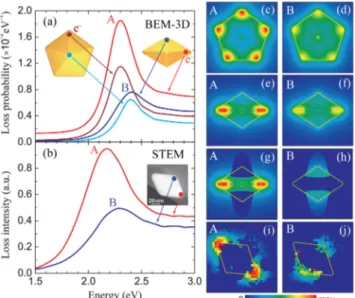
The situation is different in EELS, whose finer spatial resolution and higher intensity allows us to collect spectra from specific locations of the nanoparticle, as shown in Figure 3, and consequently resolving features A and B in both theory and experiment. This is a clear advantage of EELS in terms of sensitivity, while CL gives access to the symmetry of the mode when resolving the polarization and angular distribution of the far-field emission.43 Calculated (Figure 3a) and measured (Figure 3b) spectra are in good agreement and show that only the azimuthal mode A is efficiently excited when the electron beam is focused near the corner of the pentagonal base (red and wine curves), whereas the polar plasmon B is resolvable with the electron beam focused at the nanoparticle apex (blue
Figure 2.Cathodoluminescence spectroscopy analysis of an individual gold decahedron. (a) Calculated photon-emission probability spectra for different electron-beam probe positions (see inset). The spectra were calculated for an electron energy of 40 keV. The emission is collected over the upper hemisphere. The photon emission probability is given per incoming electron and per photon energy range. The interaction of the nanoparticle with the electron beam leads to excitation of azimuthal (A) and polar (B) plasmon modes. (b) Experimental SEM-CL photon-emission intensity spectrum for the electron beam positioned close to the particle center. Only the azimuthal mode A can be resolved in the measurement. The inset shows a SEM image of the decahedron. (c,d) Calculated photon emission probability maps of modes A and B as a function of the electron probe position. The decahedron side length is 58 nm in all cases.
and cyan curves). Note that these A and B EELS features truly reflect the near field, so they are slightly blue-shifted with respect to far-field DFM and CL measurements due to the damped nature of the plasmons.44
We now construct plasmon maps by registering the EELS probability as a function of beam position over the sample.25 Simulated maps of modes A and B are shown in Figure 3c−h for two different projections of the decahedron. Significant variations in the intensity are observed. Interestingly, these maps are in good agreement with the calculated near-field distributions and CL maps shown in Figures 1 and 2 (i.e., they show significant enhancement in the loss probability at the pentagonal base corners and the particle apexes for the azimuthal and polar modes, respectively). Because the energy difference between the two modes is smaller than the typical full width at half-maximum (fwhm), the EELS map of each plasmon mode is actually a combination of both mode spatial distributions. To overcome this problem, we constructed maps of the plasmon modes in Figure 3g,h separated in such a way that only the intensity of the dominant mode is represented for each beam position. The weight of each mode is obtained by fitting the spectrum for each image pixel to two Lorentzians plus a smooth background. For example, Figure 3h shows nonvanishing intensity of mode B only in points where it has stronger weight in the spectrum, and the map intensity is set to zero elsewhere. Likewise, Figure 3g shows the intensity where mode A is dominant. The corresponding measured STEM-EELS maps, obtained by rastering the electron beam over the decahedron and fitting the spectra as explained above, are
shown in Figure 3i,j. The spatial localizations of modes A and B are resolved with nanometer resolution and are in excellent agreement with simulations (Figure 3g,h). Now, the maximum intensity of the polar mode B is about half the value of the intensity of the azimuthal mode in both experiment and theory (see common intensity scale). In summary, this ratio is evolving from 1/10, to 1/4, and 1/2 in DFM, CL, and EELS, respectively.
So far we have presented simulations without explicit account of substrate effects, as we focused on understanding the origin and structure of individual-nanodecahedra plasmons. However, these particles are likely to be supported on one of their faces, which can undergo strong interaction with the substrate, resulting in splitting of degenerate modes. We examine this effect in Figure 4 for a 65 nm side-length gold decahedron
whose pentagonal base corners 4 and 5 are touching the mica substrate. All measured STEM-EELS spectra acquired at the five corners of the pentagonal base are dominated by dipolar azimuthal modes, as in Figure 3b (red curve). However, two distinct azimuthal plasmon modes emerge, slighty separated in energy and dominating different corners: one of them is dominant in the two corners in contact with the substrate, and the other one is stronger in the remaining three corners. These are bonding and antibonding hybridized plasmons involving substrate polarization.45−47 Excellent agreement between simulated (Figure 4a) and measured (Figure 4b) spectra is observed. Detailed plasmon maps at the energies of these features also reveal a concentration near corners either in contact or far away from the substrate in both theory (Figure 4c,d) and experiment (Figure 4e,f). Incidentally, the relative intensity of C1 and C2 features is not well captured in the simulations because we introduce a 2 nm separation between the nanoparticle surface and the substrate to improve convergence.
Plasmon broadening in the gold decahedra so-far considered can mask or even mix different modes that might be revealed
Figure 3.Electron energy-loss spectroscopy analysis of an individual gold decahedron. (a) Calculated EELS spectra for different electron beam positions (see insets). The electron energy is 100 keV. The loss probability is given per incoming electron and per electronvolt of electron-energy-loss range. The interaction of the nanoparticle with the electron beam leads to excitation of azimuthal (A) and polar (B) plasmon modes. (b) Experimental STEM-EELS spectra for electron beam positions close to either a corner of the pentagonal base (red curve) or an apex (blue curve) of the nanodecahedron. The azimuthal (A) and polar (B) modes are both unveiled by EELS. (c−h) Calculated EELS probability maps of the azimuthal (left column) and polar (right column) modes as a function of electron probe position. (i,j) Corresponding experimental EELS intensity maps with each pixel associated with a different position of the electron beam. The decahedron side length is 58 nm in all cases.
Figure 4.Comparison of theoretical (a) and experimental (b) EELS spectra showing azimuthal plasmon modes in a 65 nm side-length gold decahedron supported by a mica substrate (ε = 2.3). Two modes (C1 and C2) are clearly resolved. Calculated (c,d) and measured (e,f) maps of these modes are provided. Spectra for different corners (see number labels in the insets) are given (see labels 1−5). Mode C1 has larger strength near the corners in direct contact with the substrate, in contrast to mode C2.
Nano Letters Letter
dx.doi.org/10.1021/nl301742h| Nano Lett. 2012, 12, 4172−4180
uponfiner inspection of particles with lower losses. From the C5vsymmetry of these particles, five different plasmon modes
should be expected: two pairs of degenerate modes and a nondegenerate one. In order to understand the nature of these modes and motivated by the recent synthesis of silver decahedra48and by the fact that silver is less dissipative than gold (leading to more clearly defined plasmon bands), we simulated an individual silver particle of the same size as the above gold particles in vacuum, as shown in Figure 5a−c for
DFM, CL, and EELS. In contrast to gold (Figure 3b), several SP resonances are revealed by EELS (Figure 5c). We focus our discussion on thefive lower-energy SP modes (features i−v), because the loss structure emerging at larger energy is connected to higher-order losses, eventually approaching the classical-surface plasmon energy, and thus of less practical importance. The EELS maps associated with these modes (Figure 5d−h) exhibit rich, complex spatial distributions with 5-fold symmetry. As we show next, these plasmon modes can
be classified upon examination of their respective induced surface charges.
In a simplified tight-binding model, we can assume that these plasmons are a combination of corner-bound states. Using a quantum-mechanical notation, we consider one state |n⟩ localized at each of the corners n = 1−5, assuming a common central frequencyω0for all of them plus some interaction V
between adjacent corners. In the spirit of the tight-binding model, we describe this interaction by a 5 × 5 matrix of elements ⟨n|V|n′⟩ = −Δ for |n−n′| = 1 or 4, where Δ is a hopping frequency, and⟨n|V|n′⟩ = 0 otherwise. Five modes are then predicted upon diagonalization of this matrix, consistent with group symmetry theory: one nondegenerate mode at frequencyω0− 2Δ with equal weight in all corners, along with
two sets of doubly degenerate modes at frequenciesω0+ (1 + η)Δ and ω0 − ηΔ with weights as shown in the schemes of
Figure 6 (left part). Here,η = (√5 − 1)/2 ≈ 0.62, and for simplicity we write it as 0.6 in thefigure. We show in the right part of Figure 6 several maps corresponding to frequency-resolved components of the phase of the charge density induced by a passing electron. These phase maps are related to the EELS excitation maps atfixed frequency shown in Figure 5d−h, using the same labeling convention (i−v). We note that the EELS maps always have 5-fold symmetry because they represent the EELS response at each beam position, which is the same for each of thefive particle corners, while the induced charge maps are obtained from the response for afixed position of the electron beam. In particular, for modes i and ii, corresponding to the same features shown in Figure 5d,e, the maps clearly show the same symmetry as the right-hand-side states of the degenerate pairs, which are the only ones excited because they have mirror symmetry along the vertical axis, as the electron beam is placed at the upper corner. This leads to an effective attractive interaction energy ℏΔ ≈ 0.08 eV. Interestingly, these modes (i and ii) are clearly associated with charge pileup near the corners, and the overall sum of the charges is zero. In contrast, the fully symmetric mode at frequency ω0 − 2Δ has a nonzero net charge, so that it is
unphysical, and consequently, it does not show up in the spectrum. Incidentally, the base functions used for the corners involve positive charge accumulation, as shown at the bottom of Figure 6.
We apply a similar analysis to explain edge modes iii−v, the phase maps of which are also shown in Figure 6. In contrast to corner modes, now the base functions have zero net charge with a− + − profile along each individual edge (see bottom of Figure 6). In this case, all sets of modes are observed in the spectra, including the symmetric one, which now involves zero total charge. Incidentally, the attractive interaction for edge modes isℏΔ ≈ 0.1 eV, as extracted from the energy position of features iii−v in the spectra. Interestingly, only modes i and iv (i.e., those at energiesω0− ηΔ) display a dipole moment, and
therefore they dominate the optical scattering spectra of Figure 5a.
Conclusion. We have investigated the plasmonic properties of chemically synthesized individual gold nanodecahedra by the combined use of DFM, CL, and EELS. All of these techniques grant us access into some of the plasmon modes supported by these nanoparticles. Specifically, two dipolar modes have been identified with polarizations along the particle 5-fold symmetry axis (polar mode) and the plane perpendicular to that axis (azimuthal mode), respectively. The latter appears to have larger dipole strength, and thus it couples more strongly to
far-Figure 5. Simulated DFM, CL, and EELS spectra of an individual silver decahedron. (a) Scattering cross-section for incident-light electric field polarized parallel (red curve), perpendicular (blue curve), or under 45° (green curve) relative to the decahedron pentagonal base, as shown in the inset. (b) CL photon-emission probability spectra for different electron beam positions (see inset). The emission probability is given per incoming electron and per unit of photon energy range. The electron energy is 100 keV. (c) EELS spectra under the same conditions as in (b). The loss probability is given per incoming electron and per electronvolt of electron-energy loss range. (d−h) EELS excitation-intensity maps (linear color scale). The decahedron side length is 58 nm.
field radiation. This is why it dominates all measured spectra in DFM and CL. Our simulations, in excellent agreement with experiment, support this view, though they suggest directions of light or electron-beam incidence that permit resolving the weaker polar mode. In contrast, EELS spectra acquired with the electron beam passing near one of the two particle apexes directly reveal the presence of the polar mode. This is because EELS collects all losses regardless whether they go into radiation emission (this contributes to both plasmon CL and EELS) or absorption at the particle (this contributes only to EELS). Furthermore, we have analyzed the symmetry of these modes to understand their interplay within the particle and the energy splitting occurring due to the asymmetric interaction between the particle and a substrate. A similar analysis reveals the presence of several plasmon modes that should be resolvable in less absorptive silver particles of similar size. From our comparative analysis between all three techniques used, we conclude that EELS presents a unique combination of energy and space resolution with the ability of detecting dark modes and weak dipole plasmons more efficiently.
Methods. Synthesis of Au Decahedra. The gold nano-decahedra studied in this work were synthesized following a previously reported protocol.41,42 Briefly, a growth solution containing 0.825 mL of aqueous HAuCl40.1136 M in 15 mL of
poly(vinylpyrrolidone) (PVP, Mw = 40 000 g/mol) 2.5 mM in
N,N-dimethyl-formamide (DMF) was prepared and ultrasoni-cally irradiated until the Au3+ charge transfer to the solvent absorption band at 325 nm completely disappeared. This was followed by the addition and further sonication of varying volumes of preformed small monodisperse penta-twinned gold
seeds (2−3 nm), leading to gold bipyramids of up to 80 nm side length. This procedure allows synthesizing high-quality decahedra with narrow size and shape distributions.
Dark-Field Microscopy and Spectroscopy. DFM allows for a simple access to the far-field scattering of single metallic nanoparticles. In an optical microscope, white light is sent through a high numerical aperture dark-field condenser and focused on the sample plane, consisting of nanoparticles placed on a microscope slide. The light scattered by the dispersed nanoparticles (seen as diffraction-limited spots) is collected by an objective of lower numerical aperture and directed to a CCD camera coupled to a spectrometer. In this way, the far-field scattering spectrum of single gold decahedra can be measured. Gold nanodecahedra were first deposited on a poly-(methylmethacrylate) (PMMA, Mw= 120 000 g/mol, Aldrich) layer, which was in turn deposited on cleaned indium tin oxide coated glass substrates (Delta Technologies, Ltd.).40 Then, optical scattering spectra of the nanoparticles were acquired using a 100 W halogen lamp illumination source on a Nikon Eclipse TE-2000 inverted optical microscope coupled to a Nikon dark-field condenser (Dry, 0.95−0.80 NA). The scattered light from each nanoparticle was collected with a Nikon Plan Fluor ELWD 40×/0.60 NA objective and focused onto the entrance slit of a MicroSpec 2150i imaging spectrometer coupled to a TE-cooled CCD camera (PIXIS 1024B ACTON Princeton Instruments). The light scattered by a single decahedron was recorded in a dark-field microscope with collection times ranging from 20 to 60 s, depending on the scattering efficiency of the particles. Subsequent identification
Figure 6.Symmetry and energy of azimuthal plasmon modes in a silver nanodecahedron according to the analytical model discussed in the main text. Within a tight-binding approach with hoppingΔ between nearest neighbors in a pentagonal configuration, we obtain the states schematically shown in the left part of thisfigure, along with the energies shown in the vertical scale, where for simplicity we write 0.6 instead of (√5 − 1)/2 ≈ 0.62, and similarly for other numbers. The contour plots on the right show the phase of the induced charge at the frequency of corner and edge modes (corresponding to features i−v in the spectra of Figure 5), as produced by a beam spot at the position shown by a red circle in the lower plots. The basis functions for corner and edges modes are also shown in the lower plots. In contrast to the rest of the modes, the symmetric corner mode is unphysical because it involves a nonzero net charge on the particle, and therefore, it is not observed in the spectra. Incidentally, antisymmetric modes (with 0 value in the upper part) are not excited due to the position chosen for the electron beam.
Nano Letters Letter
dx.doi.org/10.1021/nl301742h| Nano Lett. 2012, 12, 4172−4180
and imaging by SEM (xT Nova NanoLab) was performed on the particles whose spectra were previously recorded.
Cathodoluminescence. The experimental setup used to perform our CL experiments consists of a SEM (CamScan CS3200 with LaB6 cathode), a hyperspectral light collection system, and a spectrum analyzer for the collection and analysis of the electron-induced radiation emission (EIRE).49 The electron beam was focused onto the sample via a small hole in a parabolic mirror mounted directly above it. The mirror collects the light emitted from the sample over approximately half of the available hemispherical solid angle and directs it out of the SEM chamber to a spectrum analyzer with a liquid-nitrogen-cooled CCD detector. From the measured data, it is possible to extract spectral and spatial information about the sample. In the present study, 58 nm gold decahedra deposited on a mica substrate were illuminated by an electron beam with an acceleration voltage of 40 kV and a current of 4.5 nA. The beam spot was ∼25 nm, the energy resolution of the light detector was∼2.4 meV, and the collection time was ∼2 s per spectra. Separate measurement of substrate light emission far from the nanoparticle enabled background subtraction.
Electron Energy-Loss Spectroscopy. EELS was performed on a STEM-VG HB 501 operating at 100 kV under electron-beam indicence normal to the sample and equipped with a Gatan 666 spectrometer and a homemade 2D CCD camera. The size of the focused electron-beam spot was 0.7 nm and the energy resolution in the raw data was 0.4 eV. EELS data were acquired in spectral-imaging mode by scanning the focused electron beam with a constant spatial step of 1−4 nm over two-dimensional regions (32× 32 pixels) of the sample deposited on a mica substrate. At each point of the raster, 60 spectra/pixel were taken at a rate of 3 ms per spectrum. The resulting spectral image was then stored for further treatment and analysis. In parallel, a high-angle annular dark-field signal, which is directly proportional to the projected mass in the beam direction, was acquired during the scan.50 The simultaneous acquisition of spectroscopic and topographic information enables an unambiguous assignment of a specific EELS signal to each nanovolume element. The spectra were a posteriori aligned to match their zero-loss peaks, summed up, and deconvoluted from their point spread function.51This allows both to increase the energy resolution to 0.3 eV and to remove the background due to elastically scattered electrons. For each spectrum of the spectral image, relevant information on peak energies and intensities of the surface plasmon modes were automatically extracted and subsequentlyfitted with Gaussian profiles.25 EELS intensity maps were finally generated as a function of beam position over the sample.
In particular, for gold decahedra the energy separation between different features is very small (less than the fwhm of each peak), a situation that is common in small gold nanoparticles,52 so that only one Gaussian peak is fitted per pixel in the spectral image. Then, the intensity map for a given mode is generated by setting to zero all pixels in which the fitted energy value is different from the nominal peak resonance by±0.05 eV.
Theoretical Modeling. Simulations of the electromagnetic response of individual gold decahedra were carried out using BEM,53,54which is in good agreement with additional discrete-dipole approximation (DDA) calculations (not shown),46,55 except for penetrating trajectories that have been only handled via BEM. These two methods are based upon rigorous solution of Maxwell’s equations in frequency space, assuming that the
materials involved in the structure are described in terms of local, frequency-dependent dielectric functions.
Here, we are interested in three different physical processes, specifically, light scattering upon external optical illumination, light emission induced by fast electrons, and energy losses suffered by the electrons transmitted through or near individual nanoparticles. The induced far-field in the kr → ∞ limit can be written as = Ω E r e r f ( ) ( ) ikr ind (1)
where k =ω/c and ω are the light wave vector and frequency, respectively,Ω denotes the orientation of the detector position r, and f is the far-field amplitude. The latter is directly related to the angle-resolved scattering cross-section via6
σ Ω = | Ω | | | f E d d ( )2 ext 2 (2)
for incident radiation of externalfield Eext.
We obtain the CL intensity from the Poynting vector integrated over emission directions upon interaction with a classical electron moving along a straight-line trajectory. The emitted energy per incoming electron is then given by20
∫
∫
∫
∫
π ω ω ω Δ = Ω ̂· × = ℏ ΩΓ Ω ∞ E c tr r E r t H r t 4 d d [ ( , ) ( , )] d d ( , ) rad 2 0 CL (3) where ω π Γ Ω = ℏk| Ω |f ( , ) 1 4 ( ) CL 2 2 (4)represents the number of photons emitted per incoming electron and per unit of time, solid angle of emissionΩ, and photon frequency range at frequencyω.
The energy loss suffered by a fast electron moving with constant velocity v and impact parameter b with respect to a sample reference point (e.g., the center of the nanoparticle) along a straight-line trajectoryre(t) =b + vt can be related to the force exerted by the induced electricfield Eindacting back on the electron as20
∫
∫
ω ω ω Δ = · = ℏ Γ ∞ v E r E e dt ind[ ( ), ]e t t d ( ) 0 EELS (5)where the−e electron charge has been included, so that ΔE > 0 with this definition, and
∫
ω π ω ω Γ = ℏ · ω − v E r e t e t ( ) d Re{ i t [ ( ), ]} EELS ind e (6)is the loss probability per unit of frequency loss range. We have introduced the substrate in our simulations by assuming an approximate electrostatic interaction of the structure with the image charges. Therefore, each surface-induced charge dQjused in BEM to describe a surface element j
is interacting with all induced charges dQj′× (1 − εsub)/(1 + εsub) placed at the specular reflection of the true boundary
charges with respect to the substrate plane. The total applied field thus becomes the sum of the field produce by actual and image charges.56 An effective metal-substrate separation of 2 nm was used.
Once the solution of Maxwell’s equations is found, the electromagnetic near- and far-fields induced by external plane-wave or fast-electron excitation are calculated. From the knowledge of the induced fields, we integrate eqs 2 and 4 over scattering/emission angles to obtain light scattering cross sections and CL intensities, respectively. Likewise, we integrate eq 6 over the time along the trajectory inside each medium visited by the electron to obtain EELS intensities. We focus on a self-standing gold decahedron of 58 nm side length, unless otherwise stated. Geometrical parameters for each nanoparticle (side length and curvatures of bipyramid pentagonal base corners and apexes) are obtained from SEM/TEM images. The dielectric function of gold and silver is taken from measured optical data.57
■
AUTHOR INFORMATIONCorresponding Author
*E-mail: (V.M.) V.Myroshnychenko@csic.es; (F.J.G.d.A.) J.G. deAbajo@csic.es.
Notes
The authors declare no competingfinancial interest.
■
ACKNOWLEDGMENTSWe acknowledge support from the European Union (NMP4-2006-016881-SPANS, NMP4-SL-2008-213669-ENSEMBLE, FP7-ICT-2009-4-248909-LIMA, and FP7-ICT-2009-4-248855-N4E), the Spanish MICINN (14885, MAT2010-15374, and Consolider NanoLight.es), and Ibercivis. V.M. acknowledges the Spanish CSIC - JAE grant. G.A. and N.I.Z. acknowledge support of the EPSRC and the Royal Society (London). L.M.L.-M. acknowledges funding from the ERC (Advanced Grant PLASMAQUO, 267867).
■
REFERENCES(1) Myroshnychenko, V.; Rodríguez-Fernández, J.; Pastoriza-Santos, I.; Funston, A. M.; Novo, C.; Mulvaney, P.; Liz-Marzán, L. M.; García de Abajo, F. J. Chem. Soc. Rev. 2008, 37, 1792−1805.
(2) Kelly, K. L.; Coronado, E.; Zhao, L. L.; Schatz, G. C. J. Phys. Chem. B 2003, 107, 668−677.
(3) Burda, C.; Chen, X.; Narayanan, R.; El-Sayed, M. A. Chem. Rev. 2005, 105, 1025−1102.
(4) Liz-Marzán, L. M. Langmuir 2006, 22, 32−41. (5) Noguez, C. J. Phys. Chem. C 2007, 111, 3806−3819.
(6) Bohren, C. F.; Huffman, D. R. Absorption and Scattering of Light by Small Particles; Wiley-Interscience: New York, 1983.
(7) Kreibig, U.; Vollmer, M. Optical Properties of Metal Clusters; Springer-Verlag: Berlin, 1995.
(8) Barnes, W. L.; Dereux, A.; Ebbesen, T. W. Nature 2003, 424, 824−830.
(9) Krenn, J. R.; Dereux, A.; Weeber, J. C.; Bourillot, E.; Lacroute, Y.; Goudonnet, J. P.; Schider, G.; Gotschy, W.; Leitner, A.; Aussenegg, F. R.; Girard, C. Phys. Rev. Lett. 1999, 82, 2590−2593.
(10) Maier, S. A.; Kik, P. G.; Atwater, H. A.; Meltzer, S.; Harel, E.; Koel, B. E.; Requicha, A. A. G. Nat. Mater. 2003, 2, 229−232.
(11) Manjavacas, A.; García de Abajo, F. J. Nano Lett. 2009, 9, 1285− 1289.
(12) Li, K. R.; Stockman, M. I.; Bergman, D. J. Phys. Rev. Lett. 2003, 91, 227402.
(13) Righini, M.; Ghenuche, P.; Cherukulappurath, S.; Myroshnychenko, V.; García de Abajo, F. J.; Quidant, R. Nano Lett. 2009, 9, 3387−3391.
(14) Bharadwaj, P.; Novotny, L. Opt. Express 2007, 15, 14266− 14274.
(15) Kneipp, K.; Wang, Y.; Kneipp, H.; Perelman, L. T.; Itzkan, I.; Dasari, R. R.; Feld, M. S. Phys. Rev. Lett. 1997, 78, 1667−1670.
(16) Nie, S.; Emory, S. R. Science 1997, 275, 1102−1106.
(17) Xu, H.; Bjerneld, E. J.; Käll, M.; Börjesson, L. Phys. Rev. Lett. 1999, 83, 4357−4360.
(18) Jiang, J.; Bosnick, K.; Maillard, M.; Brus, L. J. Phys. Chem. B 2003, 107, 9964−9972.
(19) Hartschuh, A. Ang. Chem., Int. Ed. 2008, 47, 8178−8191. (20) García de Abajo, F. J. Rev. Mod. Phys. 2010, 82, 209−275. (21) Chu, M.-W.; Myroshnychenko, V.; Chen, C.-H.; Deng, J.-P.; Mou, C.-Y.; García de Abajo, F. J. Nano Lett. 2009, 9, 399−404.
(22) Koh, A. L.; Bao, K.; Khan, I.; Smith, W. E.; Kothleitner, G.; Nordlander, P.; Maier, S. A.; McComb, D. W. ACS Nano 2009, 3, 3015−3022.
(23) Rossouw, D.; Couillard, M.; Vickery, J.; Kumacheva, E.; Botton, G. A. Nano Lett. 2011, 11, 1499−1504.
(24) Ritchie, R. H. Phys. Rev. 1957, 106, 874−881.
(25) Nelayah, J.; Kociak, M.; Stéphan, O.; García de Abajo, F. J.; Tencé, M.; Henrard, L.; Taverna, D.; Pastoriza-Santos, I.; Liz-Marzán, L. M.; Colliex, C. Nat. Phys. 2007, 3, 348−353.
(26) Boudarham, G.; Feth, N.; Myroshnychenko, V.; Linden, S.; García de Abajo, F. J.; Wegener, M.; Kociak, M. Phys. Rev. Lett. 2010, 105, 255501.
(27) Bosman, M.; Keast, V. J.; Watanabe, M.; Maaroof, A. I.; Cortie, M. B. Nanotechnology 2007, 18, 165505.
(28) Nicoletti, O.; Wubs, M.; Mortensen, N. A.; Sigle, W.; van Aken, P. A.; Midgley, P. A. Opt. Express 2011, 19, 15371−15379.
(29) Koh, A. L.; Fernández-Domínguez, A. I.; McComb, D. W.; Maier, S. A.; Yang, J. K. W. Nano Lett. 2011, 11, 1323−1330.
(30) Scholl, J. A.; Koh, A. L.; Dionne, J. A. Nature 2012, 483, 421− 428.
(31) Nordlander, P.; Oubre, C.; Prodan, E.; Li, K.; Stockman, M. I. Nano Lett. 2004, 4, 899−903.
(32) Liu, M.; Lee, T.-W.; Gray, S. K.; Guyot-Sionnest, P.; Pelton, M. Phys. Rev. Lett. 2009, 102, 107401.
(33) Yamamoto, N.; Araya, K.; Toda, A.; Sugiyama, H. Surf. Interface Anal. 2001, 31, 79−86.
(34) Yamamoto, N.; Araya, K.; García de Abajo, F. J. Phys. Rev. B 2001, 64, 205419.
(35) Gómez-Medina, R.; Yamamoto, N.; Nakano, M.; García de Abajo, F. J. New J. Phys. 2008, 10, 105009.
(36) Denisyuk, A. I.; Adamo, G.; MacDonald, K. F.; Edgar, J.; Arnold, M. D.; Myroshnychenko, V.; Ford, M. J.; García de Abajo, F. J.; Zheludev, N. I. Nano Lett. 2010, 10, 3250−3252.
(37) Hofmann, C. E.; Vesseur, E. J. R.; Sweatlock, L. A.; Lezec, H. J.; García de Abajo, F. J.; Polman, A.; Atwater, H. A. Nano Lett. 2007, 7, 3612−3617.
(38) Chaturvedi, P.; Hsu, K. H.; Kumar, A.; Fung, K. H.; Mabon, J. C.; Fang, N. X. ACS Nano 2009, 3, 2965−2974.
(39) Zagonel, L. F.; Mazzucco, S.; Tencé, M.; March, K.; Bernard, R.; Laslier, B.; Jacopin, G.; Tchernycheva, M.; Rigutti, L.; Julien, F. H.; Songmuang, R.; Kociak, M. Nano Lett. 2011, 11, 568−573.
(40) Rodríguez-Fernandez, J.; Novo, C.; Myroshnychenko, V.; Funston, A. M.; Sánchez-Iglesias, A.; Pastoriza-Santos, I.; Pérez-Juste, J.; García de Abajo, F. J.; Liz-Marzán, L. M.; Mulvaney, P. J. Phys. Chem. C 2009, 113, 18623−18631.
(41) Sánchez-Iglesias, A.; Pastoriza-Santos, I.; Pérez-Juste, J.; Rodríguez-González, B.; García de Abajo, F. J.; Liz-Marzán, L. M. Adv. Mater. 2006, 18, 2529−2534.
(42) Pastoriza-Santos, I.; Sánchez-Iglesias, A.; García de Abajo, F. J.; Liz-Marzán, L. M. Adv. Funct. Mater. 2007, 17, 1443−1450.
(43) Yamamoto, N.; Ohtani, S.; García de Abajo, F. J. Nano Lett. 2011, 11, 91−95.
(44) Zuloaga, J.; Nordlander, P. Nano Lett. 2011, 11, 1280−1283. (45) Zhang, S.; Bao, K.; Halas, N. J.; Xu, H.; Nordlander, P. Nano Lett. 2011, 11, 1657−1663.
(46) Geuquet, N.; Henrard, L. Ultramicroscopy 2010, 110, 1075− 1080.
(47) Mazzucco, S.; Geuquet, N.; Ye, J.; Stéphan, O.; Van Roy, W.; Van Dorpe, P.; Henrard, L.; Kociak, M. Nano Lett. 2012, 12 (3), 1288−1294.
Nano Letters Letter
dx.doi.org/10.1021/nl301742h| Nano Lett. 2012, 12, 4172−4180
(48) Pietrobon, B.; Kitaev, V. Chem. Mater. 2008, 20, 5186−5190. (49) Bashevoy, M. V.; Jonsson, F.; MacDonald, K. F.; Chen, Y.; Zheludev, N. I. Opt. Express 2007, 15, 11313−11320.
(50) Egerton, R. F. Electron Energy-Loss Spectroscopy in the Electron Microscope; Plenum Press: New York, 1996.
(51) Gloter, A.; Douiri, A.; Tence, M.; Colliex, C. Ultramicroscopy 2003, 96, 385−400.
(52) Rodríguez-González, B.; Attouchi, F.; Cardinal, M. F.; Myroshnychenko, V.; Stéphan, O.; García de Abajo, F. J.; Liz-Marzán, L. M.; Kociak, M. Langmuir 2012, 28, 9063−9070.
(53) García de Abajo, F. J.; Howie, A. Phys. Rev. B 2002, 65, 115418. (54) Myroshnychenko, V.; Carbó-Argibay, E.; Pastoriza-Santos, I.; Pérez-Juste, J.; Liz-Marzán, L. M.; García de Abajo, F. J. Adv. Mater. 2008, 20, 4288−4293.
(55) Henrard, L.; Lambin, P. J. Phys. B: At. Mol. Opt. Phys. 1996, 29, 5127−5141.
(56) Jackson, J. D. Classical Electrodynamics; Wiley: New York, 1999. (57) Johnson, P. B.; Christy, R. W. Phys. Rev. B 1972, 6, 4370−4379.